

现货库存、技术资料、百科信息、热点资讯,精彩尽在鼎好!
LM1267
150 MHz I
2
C Compatible RGB Video Amplifier System
with OSD and DACs
General Description
The LM1267 pre-amp is an integrated CMOS CRT pre-amp.
The IC is I
rameters necessary to directlysetupand adjust the gain and
contrast in the CRT display. Brightness and bias can be
controlled through the DAC outputs, and is well matched to
the LM2479 and LM2480 integrated bias clamp IC.
The LM1267 pre-amp is designed to work in cooperation
with the LM246X high gain driver family.
Black level clamping of the signal is carried out directly on
the AC coupled input signal into the high impedance preamplifier input, thus eliminating the need for additional black
level clamp capacitors.
The IC is packaged in an industry standard 24-lead DIP
molded plastic package.
2
C compatible, and allows control of all the pa-
May 2002
n Programmable 110 MHz to 150 MHz bandwidth
preamplifier with full video signal parametric control
n 4 external 8-bit DACs for bus controlled Bias and
Brightness
n Suitable for use with discrete or integrated clamp, with
software configurable Brightness mixer
n Power Save (Green) Mode, 80% power reduction
n Matched to LM246X driver
Applications
n Low end 15’ and 17’ bus controlled monitors with OSD
n 1024 X 768 displays up to 85 Hz requiring OSD
capability
n Very low cost system with LM246X driver
LM1267 150 MHz I
2
C Compatible RGB Video Amplifier System with OSD and DACs
Features
n I2C compatible interface
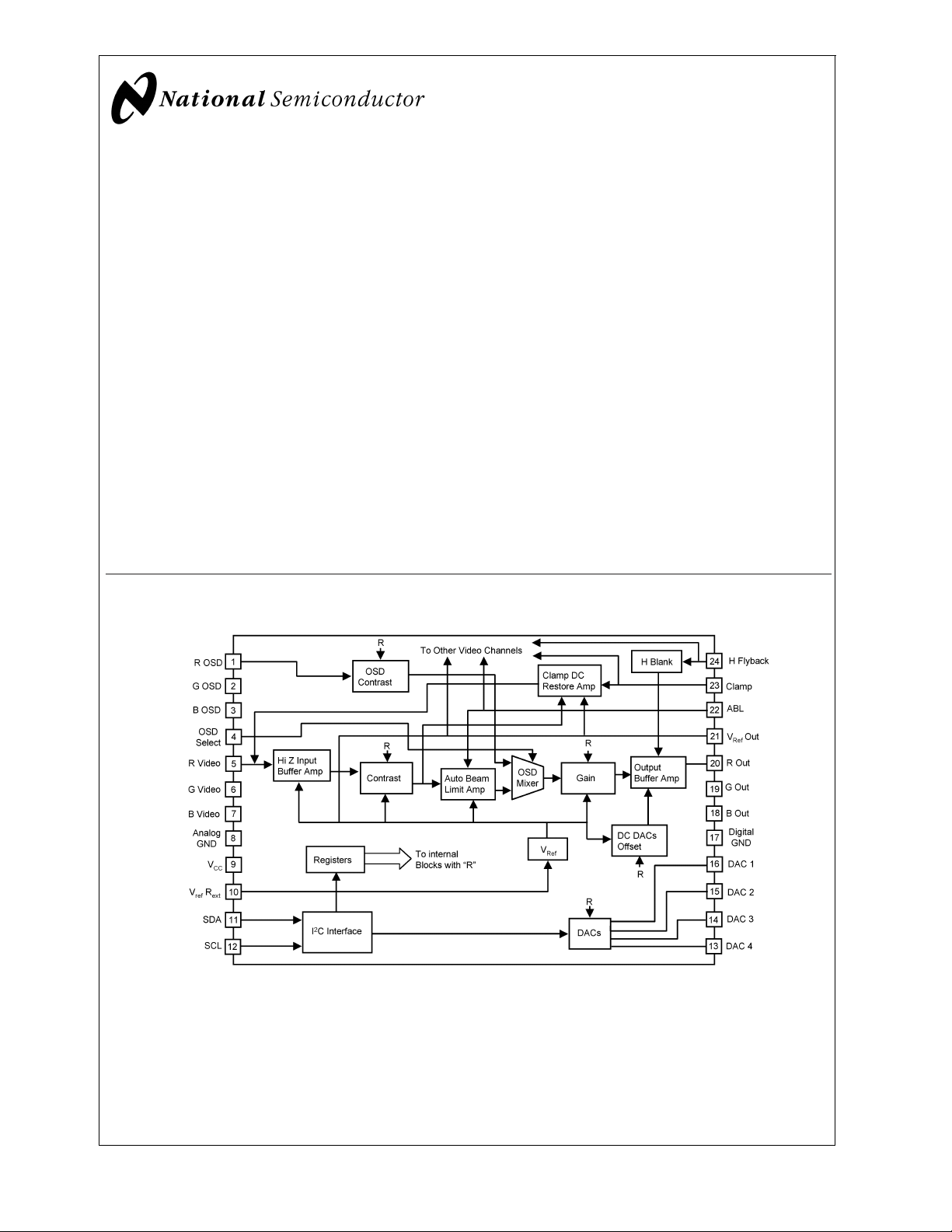
Block and Connection Diagram
FIGURE 1. Order Number LM1267NA
See NS Package Number N24D
DS200050-1
© 2002 National Semiconductor Corporation DS200050 www.national.com
Absolute Maximum Ratings (Notes 1, 3)
If Military/Aerospace specified devices are required,
LM1267
please contact the National Semiconductor Sales Office/
Distributors for availability and specifications.
Supply Voltage, Pin 9 6.0V
Peak Video Output Source Current
(Any One Amp)
Pins 18, 19, or 20 28 mA
Voltage at Any
Input Pin (V
)
IN
Power Dissipation (P
V
CC
V
IN
)
D
>
+0.5
−0.5V
>
(Above 25˚C Derate based on
and TJ) 2.4W
θ
JA
Thermal Resistance to Ambient (θ
) 51˚C/W
JA
Active Video Signal Electrical Characteristics
Unless otherwise noted: TA= 25˚C, VCC= +5V, VIN= 0.7V, V
Symbol Parameter Conditions
I
S
Maximum Supply Current Test Setting 1, RL=∞(Note
8)
I
S-PS
Maximum Supply Current,
Power Save Mode
Test Setting 1, RL=∞,Bit1of
Reg. 9 = 1 (Note 8)
LE Linearity Error Test Setting 4, Triangular
signal input source (Note 9)
V
O Blk Typ
Typical Video Black Level
Output
Test Setting 4, No AC Input
Signal, DC = 5 Hex, or 0.5V
Offset
V
O Blk Step
Video Black Level Step Size Test Setting 4, No AC Input
Signal
∆V
/∆V
O
V
O White-Max
CC
Variation in Output Video Black
Level vs V
Variations
CC
White Level Video Output
Test Setting1&3,NoAC
Input Signal, 4.75<V
Test Setting 3, Video in = 0.7V
Voltage
V
Blank
t
r
Blanked Output Level Test Setting 4, AC Input Signal 0 0.2 0.5 V
Rise Time 10% to 90%, Test Setting 4,
AC Input Signal (Note 10)
OS
R
Overshoot (Rising Edge) Test Setting 4, AC Input Signal
(Note 10)
t
f
Fall Time 90% to 10%, Test Setting 4,
AC Input Signal (Note 10)
OS
F
Overshoot (Falling Edge) Test Setting 4, AC Input Signal
(Note 10)
f(−3 dB) Video Amplifier Bandwidth
(Note 13)
V
10 kHz Video Amplifier 10 kHz
sep
Test Setting 8, Register 0Bh
Bits 2-0 Set to 111, V
V
P-P
Test Setting 8 (Note 14)
Isolation
V
10 MHz Video Amplifier 10 MHz
sep
Test Setting 8 (Note 14)
Isolation
A
V Max
1
A
⁄
2
V
A
V Min
A
V Gain
A
V Gain Min
A
V Match
1
⁄
2
Maximum Voltage Gain Test Setting 8, AC Input Signal 4 V/V
Contrast@50% Level Test Setting 5, AC Input Signal −10 dB
Maximum Contrast Attenuation Test Setting 2, AC Input Signal −20 dB
Gain@50% Level Test Setting 6, AC Input Signal −5 dB
Maximum Gain Attenuation Test Setting 7, AC Input Signal −10 dB
Absolute Gain Match@A
V Max
Test Setting 3, AC Input Signal
ABL=VCC,CL
Thermal Resistance to Case (θ
Junction Temperature (T
) 150˚C
J
) 32˚C/W
JC
ESD Susceptibility (Note 4) 3.5 kV
ESD Machine Model (Note 5) 350V
Storage Temperature −65˚C to +150˚C
Lead Temperature
(Soldering, 10 sec.) 265˚C
Operating Ratings (Note 2)
Temperature Range 0˚C to 70˚C
Supply Voltage (V
) 4.75V<V
CC
Video Inputs 0.0V
= 8 pF, Video Output = 2 V
Min
(Note 7)
Typ
(Note 6)
P-P
.
210 235 mA
45 60 mA
5%
1.05 1.25 1.45 VDC
60 90 120 mV
<
5.25
CC
−50 0 50 mV/V
4.0 4.2 V
3.0 ns
8%
3.0 ns
8%
O
= 3.5
150 MHz
−70 dB
−50 dB
±
0.5 dB
<
Max
(Note 7)
<
5.25V
CC
<
V
1.0V
IN
P-P
Units
www.national.com 2
Active Video Signal Electrical Characteristics (Continued)
Unless otherwise noted: TA= 25˚C, VCC= +5V, VIN= 0.7V, V
ABL=VCC,CL
Symbol Parameter Conditions
A
V Track
Gain Change between
Amplifiers
Tracking when Changing from
Test Setting 8 to Test Setting 5
(Note 11)
V
ABL TH
ABL Control Upper Limit Test Setting 4, AC Input Signal
(Note 12)
V
ABL Range
∆A
ABL
ABL Control Voltage Active
Range
Test Setting 4, AC Input Signal
(Note 12)
ABL Control Range Test Setting 4, AC Input Signal
(Note 12)
I
ABL Active
I
ABL Max
V
Clamp Max
V
Clamp Min
I
Clamp
t
PW Clamp
t
Clamp-Video
ABL Input Bias Current during
ABL
ABL Input Current Clamp Sink
Capability
Test Setting 4, AC Input
Signal, V
ABL
Test Setting 4, AC Input Signal
(Note 12)
Clamp Gate Low Input Voltage Clamp Comparators Off 1.4 V
Clamp Gate High Input Voltage Clamp Comparators On 2.6 V
Clamp Gate Input Current V23=0VtoVCC− 1V −5 0.1 10 µA
Back Porch Clamp Pulse Width (Note 15) 200 ns
End of Clamp Pulse to Start of
Limit is guaranteed by design
Active Video
R
In-Video
I
In-Video
V
Out V
Ref
Input Resistance Test Setting (4) 20 MΩ
Input Bias Current Test Setting (4) 0.1 10 µA
Output Voltage 10 kΩ, 1% Resistor; Pin 10 to
Ref
GND
V
Spot
Spot Killer Voltage VCCAdjusted to Activate 3.6 4.0 4.25 V
= 2V(Note 12)
= 8 pF, Video Output = 2 V
.
P-P
Min
(Note 7)
Typ
(Note 6)
±
0.5 dB
Max
(Note 7)
5V
2V
−8 dB
010µA
1mA
200 nsec
1.25 1.40 1.55 V
LM1267
Units
OSD Electrical Characteristics
Unless otherwise noted: TA= 25˚C, VCC= +5V, VIN= 0.7V, V
ting 8.
Symbol Parameter Conditions
V
OSD-L
OSD Input Low Input
OSD Inputs are Selected
Operating Range
V
OSD-H
OSD Input High Input
OSD Inputs are Selected
Operating Range
I
OSD
V
OSD-Sel-L
OSD Input Current V
OSD Select Low Input
OSD
Video Inputs are Selected
Operating Range
V
OSD-Sel-H
OSD Select High Input
OSD Inputs are Selected
Operating Range
I
OSD-Sel
∆V
O-OSD(Blk)
OSD Select Input Current V
OSD ∆Black Level Output
Voltage, Difference from Video
OSD-Sel
Register 08 = 18, Minimum
Video Black Level
Output
V
O-OSD(Blk)
Range of OSD Black Level
Output Voltage between the 3
Register 08 = 18, Minimum
Video Black Level −100 0 +100 mV
Channels
V
OSD-out
∆V
OSD-out
V
OSD-out
(Track)
OSD Output Voltage, Percent
of Maximum Video Out
OSD Output V
Attenuation Register 08 = 08 58 63 68 %
P-P
Output Variation between
Channels
Register 08 = 18, Minimum
Video Black Level
Register 08 Changed from 18
to 08
ABL=VCC,CL
=0VtoVCC− 1V −5 0.1 10 µA
=0VtoVCC− 1V −5 0.1 10 µA
= 8 pF, Video Signal Output = 2 V
Min
(Note 7)
Typ
(Note 6)
(Note 7)
2.5 V
2.5 V
±
45
75 88 100 %
±
3.0
, Test Set-
P-P
Max
1.2 V
1.2 V
±
150 mV
±
5.0 %
Units
www.national.com3
OSD Electrical Characteristics (Continued)
Unless otherwise noted: TA= 25˚C, VCC= +5V, VIN= 0.7V, V
LM1267
ABL=VCC,CL
ting 8.
Symbol Parameter Conditions
∆t
OSD/OSD S
V
10 kHz Video Feedthrough into OSD OSD Inputs = 0V −70 dB
feed
V
10 MHz Video Feedthrough into OSD OSD Inputs = 0V −60 dB
feed
Output Skew Time between
OSD and OSD Select
Measured from 50% Point on
all Waveforms
External DAC Signals Electrical Characteristics
Unless otherwise noted: TA= 25˚C, VCC= +5V, VIN= 0.7V, V
lowing apply for all four external DACs.
Symbol Parameter Conditions
V
Min DAC
V
Max DAC
Mode 00
V
Max DAC
Mode 11
∆V
Max DAC
(Temp)
∆V
Max DAC
(VCC)
Min DAC Output Voltage Value = 00h 0.5 0.75 V
Max DAC Output Voltage Value = FFh, DCF[1:0] = 00h
(no load)
Max Output Voltage of DACs
1–3 in DCF Mode 11
Variation of any DAC output
Value = FFh, DCF[1:0] = 11h,
DAC4 Value = 00h
0˚C
voltage with temperature
Variation of any DAC output
voltage with V
CC
4.75V<V
Linearity Linearity of DAC Over its
Range
Monotonicity Monotonicity of the DAC Excluding dead zones at limits
of DAC
<T<
70˚C ambient
CC
ABL=VCC,CL
<
5.25V
= 8 pF, Video Signal Output = 2 V
Min
(Note 7)
Typ
(Note 6)
±
2.0 ns
(Note 7)
= 8 pF, Video Signal Output = 2 V
Min
(Note 7)
Typ
(Note 6)
(Note 7)
3.6 4.2 V
1.85 2.1 2.35 V
±
0.5 mV/deg
±
50 mV/V
5%
±
0.5 LSB
P-P
Max
P-P
Max
, Test Set-
Units
. The fol-
Units
External Interface Signals Electrical Characteristics
Unless otherwise noted: TA= 25˚C, VCC= +5V, VIN= 0.7V, V
ABL=VCC,CL
Symbol Parameter Conditions
V
(I2C) I2C Low Input Voltage SDA or SCL Inputs −0.5 0.5 1.5 V
l
V
(I2C) I2C High Input Voltage SDA or SCL Inputs 3.0 4.0 5.0 V
h
I
(I2C) I2C Low Input Current SDA or SCL Inputs, Input
l
Voltage = 0V
I
(I2C) I2C High Input Current SDA or SCL Inputs, Input
h
Voltage = 5V
t
H-Blank on
t
H-Blank off
I
In Threshold
H-Blank Time Delay from Zero
Crossing Point of H Flyback
H-Blank Time Delay from Zero
Crossing Point of H Flyback
IInH-Blank Detection
Rising Edge of the Flyback
Signal
Falling Edge of the Flyback
Signal
Threshold
I
In-Operating
Minimum—Insure Normal
Operation
Maximum—Should Not
Lowest Operating Horizontal
Frequency in Given Application
(Note 17)
Exceed in Normal Operation
I
In Flyback
Peak Current during Flyback
Period, Recommended Design
Range
Operating Range for all
Horizontal Scan Frequencies,
Maximum Current Should Not
Exceed 2 mA (Note 17)
Note 1: Limits of Absolute Maximum Ratings indicate limits below which damage to the device must not occur.
Note 2: Limits of operating ratings indicate required boundaries of conditions for which the device is functional, but may not meet specific performance limits.
= 8 pF, Video Output = 2 V
Min
(Note 7)
Typ
(Note 6)
1.9 2.2 2.5 µA
0.3 0.6 0.9 µA
50 ns
50 ns
−20 µA
−30 −300 µA
0.5 1.5 2.0 mA
P-P
.
Max
(Note 7)
Units
www.national.com 4
External Interface Signals Electrical Characteristics (Continued)
Note 3: All voltages are measured with respect to GND, unless otherwise specified.
Note 4: Human body model, 100 pF discharged through a 1.5 kΩ resistor.
Note 5: Machine Model ESD test is covered by specification EIAJ IC-121-1981. A 200 pF cap is charged to the specified voltage, then discharged directly into the
IC with no external series resistor (resistance of discharge path must be under 50Ω).
Note 6: Typical specifications are specified at +25˚C and represent the most likely parametric norm.
Note 7: Tested limits are guaranteed to National’s AOQL (Average Outgoing Quality Level).
Note 8: The supply current specified is the quiescent current for V
the supply current is used by the pre-amp.
Note 9: Linearity Error is the variation in step height of a 16 step staircase input signal waveform with 0.7 V
with each step approximately 100 ns in width.
Note 10: Input from signal generator: t
generator response have been removed from the output rise and fall times.
Note 11: ∆A
gain change between any two amplifiers with the contrast set to A
track is a measure of the ability of any two amplifiers to track each other and quantifies the matching of the three gain stages. It is the difference in
V
<
1 ns. Scope and generator response used for testing: tr= 1.1 ns, tf= 0.9 ns. Using the RSS technique the scope and
r,tf
gains might be 12.1 dB, 11.9 dB, and 11.8 dB and change to 2.2 dB, 1.9 dB and 1.7 dB respectively for contrast set to A
±
10.0 dB with a tracking change of
0.2 dB.
Note 12: ABL should provide smooth decrease in gain over the operational range of 0 dB to –6 dB
∆A
= A(V
ABL
ABL=VABL Max Gain
Beyond –6 dB the gain characteristics, linearity, pulse response, and/or behavior may depart from normal values.
Note 13: Adjust input frequency from 10 MHz (A
max reference level) to the −3 dB corner frequency (f
V
Note 14: Measure output levels of the other two undriven amplifiers relative to the driven amplifier to determine channel separation. Terminate the undriven amplifier
inputs to simulate generator loading. Repeat test at f
= 10 MHz for V
IN
Note 15: A minimum pulse width of 200 ns is guaranteed for a horizontal line of 15 kHz. This limit is guaranteed by design. If a lower line rate is used then a longer
clamp pulse may be required.
Note 16: The video black level is used for this test. OSD amplitude is measured from the video black level to the OSD white level.
Note 17: Limits met by matching the external resistor going to pin 24 to the H Flyback voltage.
with RL=∞. Load resistors are not required and are not used in the test circuit, therefore all
CC
level at the input, subdivided into 16 equal steps,
P-P
1
⁄
2
and measured relative to the AVmax condition. For example, at AVmax the three amplifiers’
V
sep 10 MHz
.
) − A(V
ABL=VABL Min Gain
−3 dB
).
1
⁄
2
. This yields a typical gain change of
V
)
LM1267
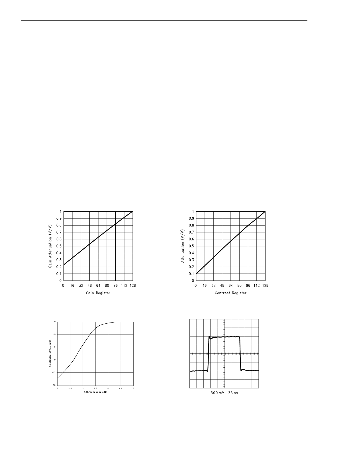
Typical Performance Characteristics V
Gain Attenuation
DS200050-2
ABL Attenuation
=5V,TA= 25˚ unless otherwise specified.
CC
Contrast Attenuation
Output Waveform
DS200050-3
DS200050-4
DS200050-5
www.national.com5
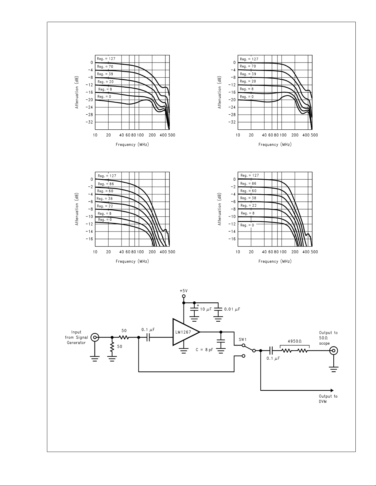
Typical Performance Characteristics V
LM1267
Contrast vs Frequency, Bandwidth = 0
= 5V, TA= 25˚ unless otherwise specified. (Continued)
CC
Contrast vs Frequency, Bandwidth = 7
Gain vs Frequency, Bandwidth = 0
Test Circuit
DS200050-6
DS200050-8
DS200050-7
Gain vs Frequency, Bandwidth = 7
DS200050-9
Note: 8 pF load includes parasitic capacitance.
www.national.com 6
DS200050-10
 Loading...