


现货库存、技术资料、百科信息、热点资讯,精彩尽在鼎好!
LM1253A
Monolithic Triple 180 MHz I
Integrated Analog On Screen Display (OSD) Generator
2
C CRT Pre-amp With
May 2000
(OSD) Generator
LM1253A Monolithic Triple 180 MHz I
General Description
The LM1253A pre-amp is an integrated high voltage triple
CRT pre-amp and Analog On Screen Display (OSD) generator. The IC is I
rameters necessary to setup and adjust the brightness and
contrast in the CRT display. In addition, it provides a programmable period vertical blanking pulse which is used to
blank the G1.
The LM1253A pre-amp is designed to work in cooperation
with the LM2453 driver, and provides a multiplexed video
signal (VideoPlex) interface to enable the DC clamp levels at
the cathode to be varied in order to set up the CRT bias and
to allow individual adjustment for brightness.
TheAnalogOSDhas a selectable palette allowing a wide selection of colors. The preset level of the OSD can be controlled by I
is internally mixed with the video signal, before the gain section, and thus gives excellent white tracking of the OSD with
the white color point setting of the video.
The Brightness settings are also mixed into the video signal
before the gain matching controls and consequently give excellent white color point tracking with variations in the Brightness control. An active horizontal blanking signal is added to
the video at the output, giving excellent smear performance,
and preventing video content dependent DC bias offsets as
a result of high frequency over shoot.
The OSD horizontal sync and blanking signal is derived from
a positive going flyback pulse. The digital section provides
easy interfacing of this signal with the deflection circuits.
The vertical blanking signal is taken from the vertical sync
signal, and the blanking duration is programmable. This system is highly integrated and requires a minimal number of
external components.
Black level clamping of the signal is carried out directly on
the AC coupled input signal into the high impedance preamplifier input, thus eliminating the need for additional black
level clamp capacitors.
2
C controlled, and allows control of all the pa-
2
C to suit different CRT displays. The OSD signal
The outputs are referenced to a DC level produced by the
LM1253A Pre-amp, and so are guaranteed to provide stable
DC operating levels within the system without the need for
additional external feedback components.
The IC is packaged in an industry standard wide body 28lead DIL molded plastic package.
Features
n 190 two-color ROM based Character Fonts
n 64 four-color ROM based Character Fonts
n Supports a programmable page size with up to 512
characters and line definition codes
n Support for 2 Display Windows (size of each window is
configurable)
n Programmable start position for each Display Window
n Programmable Resolutions: from 512 to 960 pixels per
line in 64 pixel increments
n Programmable Character Height, with automatic height
control with mode change
n Programmable Row Spacing between each display
character row
n Maximum Pixel clock of 92.2 MHz
2
n I
C compatible interface to controlling micro-controller
n Button boxes
n 180 MHz preamplifier with full video signal parametric
control
n VideoPlex
n OSD mixing with 64 out of 512 color mask
programmable selection
™
interface to the LM2453 driver
Intended Applications
n 1280 x 1024 Displays up to 75 Hz requiring OSD
capability
2
C CRT Pre-amp With Integrated Analog On Screen Display
© 2000 National Semiconductor Corporation DS101265 www.national.com

Table of Contents
Block and Connection Diagrams 3
LM1253A
Absolute Maximum Ratings 5
Operating Ratings 5
Electrical Characteristics 5
Test Circuit 7
Test Settings 8
Pin Descriptions 8
Input/Output Schematics 13
National VideoPlex Video System 15
ESD and Arc-Over Protection 16
Pre-Amp Functional Description 17
Horizontal Phase Locked Loop 19
Fault Operation 19
Power Save Mode 19
Schematics 20
PCB Layout 22
OSD Generator Operation 23
Micro-Controller Interface 27
LM1253A Address Map 29
Pre-Amp Interface Registers 30
Two-Color Attribute Table 31
Four-Color Attribute Table 31
Display Page RAM 32
Controller Register Definitions 40
Character Font 51
List of Tables
Table 1 Control Test Settings 7
Table 2 Registers Controlling the Output
Video and Clamp Signal 18
Table 3 Character ROM Address Map 29
Table 4 Display Page RAM Address Map 29
Table 5 OSD Interface Registers 30
Table 6 Pre-Amp Interface Registers 31
Table 7 Two-Color Attribute Registers 31
Table 8 Four-Color Attribute Registers 31
Table 9 Example 1 I
Table 10 Example 2 I
Table 11 Example 3 I
Table 12 PLL Setting (Register 843Eh) 46
Table 13 Attribute Tables to I
2
C Transmission 35
2
C Transmissions 36
2
C Transmissions 39
2
C Address 48
www.national.com 2
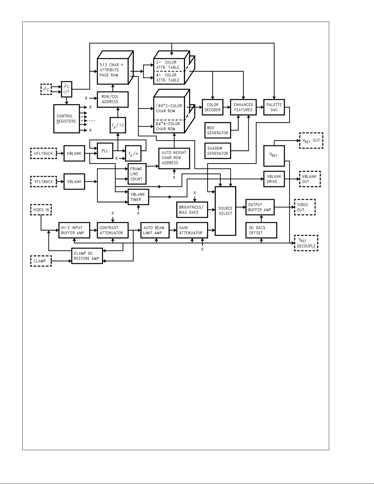
Block and Connection Diagrams
LM1253A
FIGURE 1. Block Diagram
DS101265-1
www.national.com3
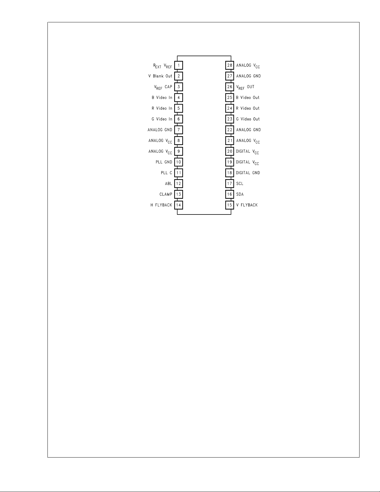
Block and Connection Diagrams (Continued)
LM1253A
28-Lead (0.600’’ wide) Molded Dual-In-Line Package
DS101265-2
Order Number LM1253AN
See NS Package Number N28B
FIGURE 2. Connection Diagram
www.national.com 4
LM1253A
Absolute Maximum Ratings (Notes 1, 3)
If Military/Aerospace specified devices are required,
please contact the National Semiconductor Sales Office/
Lead Temperature (Soldering,
ESD Tolerance, Human Body Model 3 kV
<
10 sec.) 300˚C
Machine Model 300V
Distributors for availability and specifications.
Supply Voltage, (V
Input Voltage, (V
)6V
CC
)6V
IN
Storage Temperature Range, (T
T
JMAX
) −65˚C to +150˚C
STG
150˚C
Operating Ranges (Note 2)
Temperature Range 0˚C to +70˚C
V
CC
+4.75V to +5.25V
Active Video Signal Electrical Characteristics
(See
Figure 3
Unless otherwise noted: V
Symbol Parameter Conditions
I
CC1MAX
V
OUT BLK
LE Linearity Error Test Setting 3, (Note 4), Triangular
V
OUT WHITE
t
r
t
f
OS
R
OS
F
f(−3dB) Video Amplifier Bandwidth Measured in AC2DC002 Demo
A
CONTRAST
A
GAIN
A
MAX
V
ABL TH
V
ABL RANGE
∆A
ABL
I
ABL MAX
C
IP
V
REF
XT Channel to Channel Crosstalk 10 MHz 40 dB
for Test Circuit, and
CC
Table 1
for Control Test Settings Chart)
= +5V, VIN= 0.7V, CL= 8 pF, Video Signal Output = 1 VPP,TA= 25˚C, V
ABL=VCC
.
LM1253A
Min Typ Max
Maximum Supply Current Test Setting 1, No Output Load 245 mA
Active Video Black Level Minimum
Output Voltage
Active Video White Level Max
Output Voltage
Rise Time Test Setting 3, (Note 5), 10% to
Fall Time Test Setting 3, (Note 5), 90% to
Rising Edge Overshoot Test Setting 3, (Note 5), AC Input
Falling Edge Overshoot Test Setting 3, (Note 5), AC Input
Test Setting 1, No AC Input Signal
Step Signal Input
Test Setting 3, AC Input Signal
90%, AC Input Signal
10%, AC Input Signal
Signal
Signal
Board. LM1253A set for 40 V
PP
V
REF
1%
2.7 V
3.0 ns
3.0 ns
5%
5%
180 MHz
swing at LM2453 output
Contrast Max-Min Adjustment
Range
Test Setting 2, AC Input Signal
20 dB
Gain Max-Min Adjustment Range Test Setting 2, AC Input Signal 10 dB
Max Signal Voltage Gain Test Setting 2, AC Input Signal 1.8 V/V
Auto Beam Limit Control Upper
Limit
Auto Beam Limit Control Voltage
Range
Auto Beam Limit Control Range Test Setting 3, (Note 6), AC Input
Auto Beam Limit Input Current
Sink Capability
Test Setting 3, (Note 6), AC Input
Signal
Test Setting 3, (Note 6), AC Input
Signal
Signal
Test Setting 3, (Note 6), AC Input
Signal
4.5 V
3V
−10 dB
1mA
Input AC Coupling Capacitor Test Setting 3 4.7 nF
Typical V
Output Voltage 1.55 1.65 1.75 V
REF
Units
V
DC
www.national.com5
Brightness/Bias Signal Electrical Characteristics
(See
Figure 3
Unless otherwise noted: VCC= +5V, VIN= 0.7V, CL= 8 pF, Video Signal Output = 1 VPP,TA= 25˚C, V
LM1253A
for Test Circuit, and
Table 1
for Control Test Settings Chart)
Symbol Parameter Conditions
V
BLANK MAX
V
BLANK MIN
t
BLK r
t
BLK f
OS
BLK MAX
Maximum Blanking Level Test Setting 1 V
Minimum Blanking Level Test Setting 4 V
Blanking Rise Time Test Setting 1, 10% to 90%, 10 ns
Blanking Fall Time Test Setting 1, 90% to 10%, 10 ns
Maximum Rise or Fall Edge
Overshoot
Test Setting 1, 10% to 90% or
90% to 10%, Settling Time Must
be Less Than 50 ns
OSD Electrical Characteristics
(See
Figure 3
Unless otherwise noted: VCC= +5V, VIN= 0.7V, CL= 8 pF, Video Signal Output = 1 VPP,TA= 25˚C, V
Symbol Parameter Conditions
V
OSDHIGH MAX
V
OSDHIGH 10
V
OSDHIGH 01
V
OSDHIGH 00
for Test Circuit)
Maximum OSD Level with OSD
Contrast 11
Maximum OSD Level with OSD
Contrast 10
Maximum OSD Level with OSD
Contrast 01
Maximum OSD Level with OSD
Contrast 00
Palette Set at 111. OSD Contrast
Level 11, Test Setting 3
Palette Set at 111. OSD Contrast
Level 10, Test Setting 3
Palette Set at 111. OSD Contrast
Level 01, Test Setting 3
Palette Set at 111. OSD Contrast
Level 00, Test Setting 3
ABL=VCC
.
LM1253A
Min Typ Max
REF
−
0.90
REF
20 %
ABL=VCC
.
LM1253A
Min Typ Max
V
REF
+
0.95
V
REF
+
0.77
V
REF
+
0.59
V
REF
+
0.41
Units
V
V
Units
V
V
V
V
External Interface Signals Electrical Characteristics
(See
Figure 3
Unless otherwise noted: VCC= +5V, VIN= 0.7V, CL= 8 pF, Video Signal Output = 1 VPP,TA= 25˚C, V
Symbol Parameter Conditions
I
IN−MAX
V
HBLANK TRIG
I
IN+MAX
t
min hflb
t
H
t
PW CLAMP
V
CLAMP L MAX
V
CLAMP H MIN
V
VBLANK HIGH
V
VBLANK LOW
www.national.com 6
for Test Circuit)
Maximum normal forward scan current at
lowest horizontal frequency that input can
−150 µA
withstand
Voltage on H Flyback (Pin 14) which will
Trigger an HBLANK Signal
100V H Flyback Signal
through a 100 kΩ
Resistor
Maximum flyback scan current at 125 kHz
that input can withstand
Minimum Flyback Width 1 µs
Horizontal Period 20 125 kHz
Minimum Clamp Pulse Width 200 ns
Maximum Low Level Clamp Pulse Voltage 1 V
Minimum High Level Clamp Pulse Voltage 3 V
Minimum High Level of Vertical Blank
V
VREF BLANK
<
0.75V V
Output
Maximum Low Level of Vertical Blank
I
VBLANK OUT
= 100 µA V
Output
ABL=VCC
.
LM1253A
Min Typ Max
0.8 V
1.5 mA
REF
+1
REF
−1
Units
V
V
External Interface Signals Electrical Characteristics (Continued)
(See
Figure 3
Unless otherwise noted: VCC= +5V, VIN= 0.7V, CL= 8 pF, Video Signal Output = 1 VPP,TA= 25˚C, V
Symbol Parameter Conditions
V
CCDET
F
FREE_RUN
V
IL
V
IH
V
OL
Note 1: Absolute Maximum Ratings indicate limits beyond which damage to the device may occur.
Note 2: Operating Ranges indicate conditions forwhichthedevice is functional, but do not guarantee specific performance limits. For guaranteed specifications and
test conditions, see the Electrical Characteristics. The guaranteed specifications apply only for the test conditions listed. Some performance characteristics may
change when the device is not operated under the listed test conditions.
Note 3: All voltages are measured with respect to GND, unless otherwise specified.
Note 4: Linearity Error = 100
Where: The input signal is a 16 step staircase signal waveform with 0.7 V
step
max
step
min
step
ave
Note 5: Input from signal generator: t
Note 6: ABL should provide smooth decrease in gain over the operational range of 0 dB to −5 dB
∆A
= A(V
ABL
for Test Circuit)
VCCUndervoltage Detection Threshold 3.9 V
Free Run HBLANK Frequency 30 60 kHz
Low Level Input Voltage for SDA and SCL
Pins
High Level Input Voltage for SDA and SCL
Pins
Low Level Output Voltage for SDA and SCL
Pins
*
(step
–step
max
is the maximum voltage step at the output
is the minimum voltage step at the output
is the average voltage of the 16 steps at the output.
ABL=VABL MAX GAIN
)–A (V
)/step
min
<
1 ns.
r,tf
ABL=VABL MIN GAIN
ave
ABL=VCC
.
LM1253A
Min Typ Max
1.5 V
3V
3 mA Sink Current
level, subdivided into 16 equal steps, with each step approximately 100 ns in width
P-P
)
0 0.4 V
LM1253A
Units
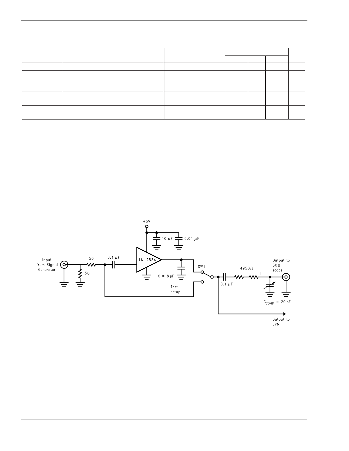
Test Circuit
Note: 8 pF load includes parasitic capacitance
DS101265-3
FIGURE 3. Test Circuit
www.national.com7
Test Settings
LM1253A
No.
Control
of
Bits
Setting 1
Contrast 7 Max
R,G,B Gain 7 Max
Brightness 8 Max
R,G,B Bias 8 Max
DC Offset 3 Min
Pedestal Offset 3 Max
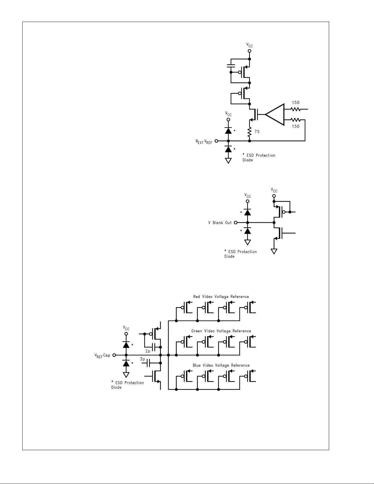
Pin Descriptions
Pin 1—R
EXTVREF
pin to set up the internal current sources. The LM1253A is
optimized for this value of resistor. A DC voltage only will be
on this pin. Decreasing the value of this resistor will increase
supply current while degrading performance; increasing the
value of the resistor will decrease supply current and also
degrade the performance. Do not place the resistor close to
sources of heat such as the CRT driver.
components connected to pin 1,
schematic of pin 1.
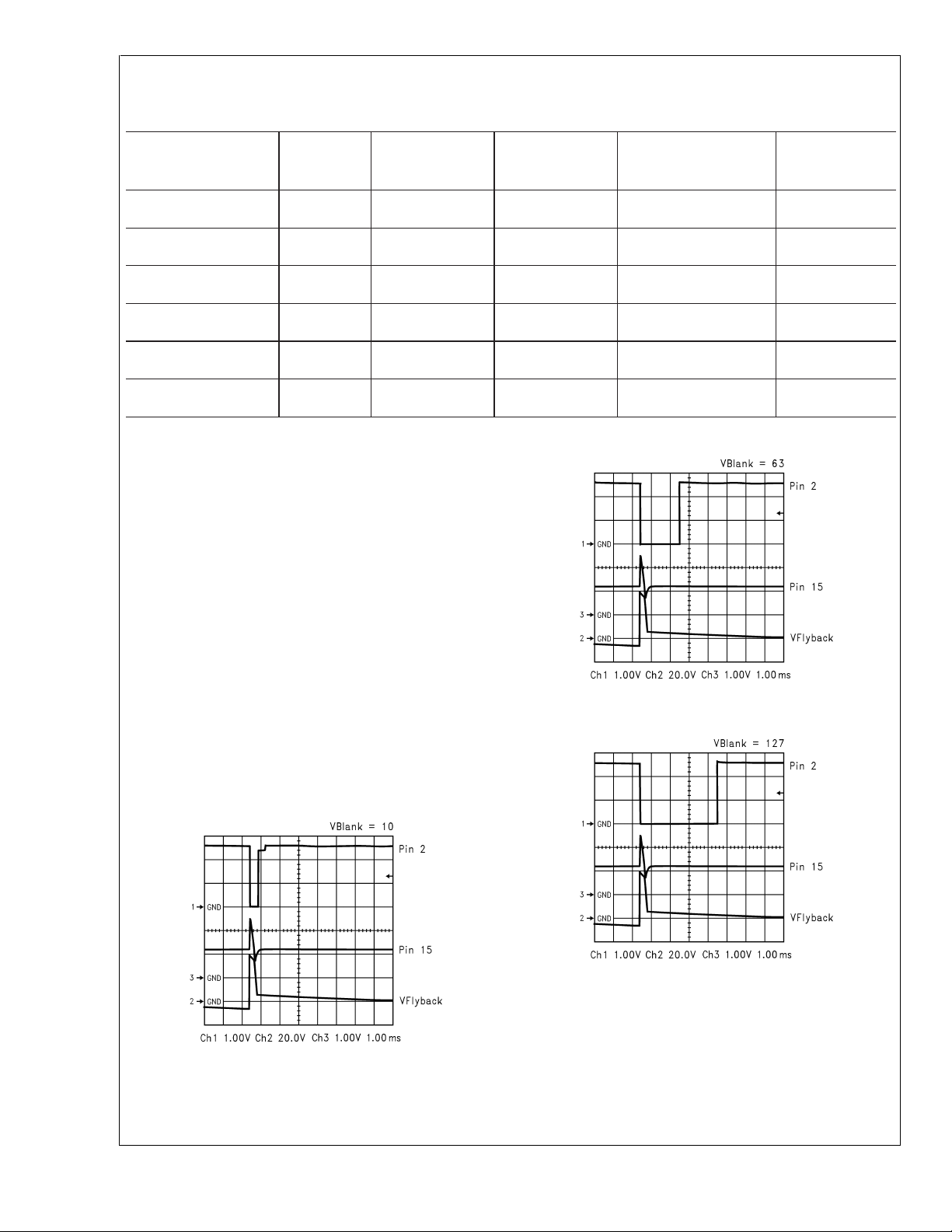
Pin 2—V Blank Out This pin supplies a variable width,
negative going pulse at the vertical rate to the CRT Driver. V
Blank is triggered from the signal on pin 15, which comes
from the vertical flyback. The CRT Driver supplies the pull up
for this pin. The width of this pulse is set by the value in the
VBLANKDUR register (8403h).
sulting V Blank Out pulse with various values in register
8403h. The trace connecting pin 2 of the LM1253A to the
LM2453 must be kept away from the output circuitry of the
LM2453.
Figure 12
Figure 29
shows the internal schematic of pin 2.
A10kΩ1% resistor is connected to this
Figure 29
Figure 11
shows the internal
Figures 4, 5, 6
shows the external schematic of pin 2,
TABLE 1. Control Test Settings
Basic
Test
Basic
Test
Setting 2
Max
(Hex 7F)
(Hex 7F)
Max
(Hex 7F)
(Hex 7F)
Max
(Hex FF)
(Hex FF)
Max
(Hex FF)
(Hex FF)
Max
(Hex 07)
(Hex 00)
Max
(Hex 07)
(Hex 07)
shows the
show the re-
Basic
Test
Setting 3
Max
(Hex 7F)
Set for 1 V
P-P
on all Channels
Min
(Hex 00)
Min
(Hex 00)
Min
(Hex 07)
Min
(Hex 00)
FIGURE 5. V Blank = 63
Basic
Test
Setting 4
Max
(Hex 7F)
Max
(Hex 7F)
Min
(Hex 00)
Min
(Hex 00)
Min
(Hex 07)
Min
(Hex 00)
DS101265-8
DS101265-7
FIGURE 4. V Blank = 10
www.national.com 8
DS101265-9
FIGURE 6. V Blank = 127
Pin 3—V
pin to decouple V
nel circuits to make the VideoPlex signal.
the external schematic of pin 3,
Cap A 0.1 µF capacitor is placed close to this
REF
REF.VREF
is used by the three video chan-
Figure 29
Figure 13
shows the internal
shows
schematic of pin 3.
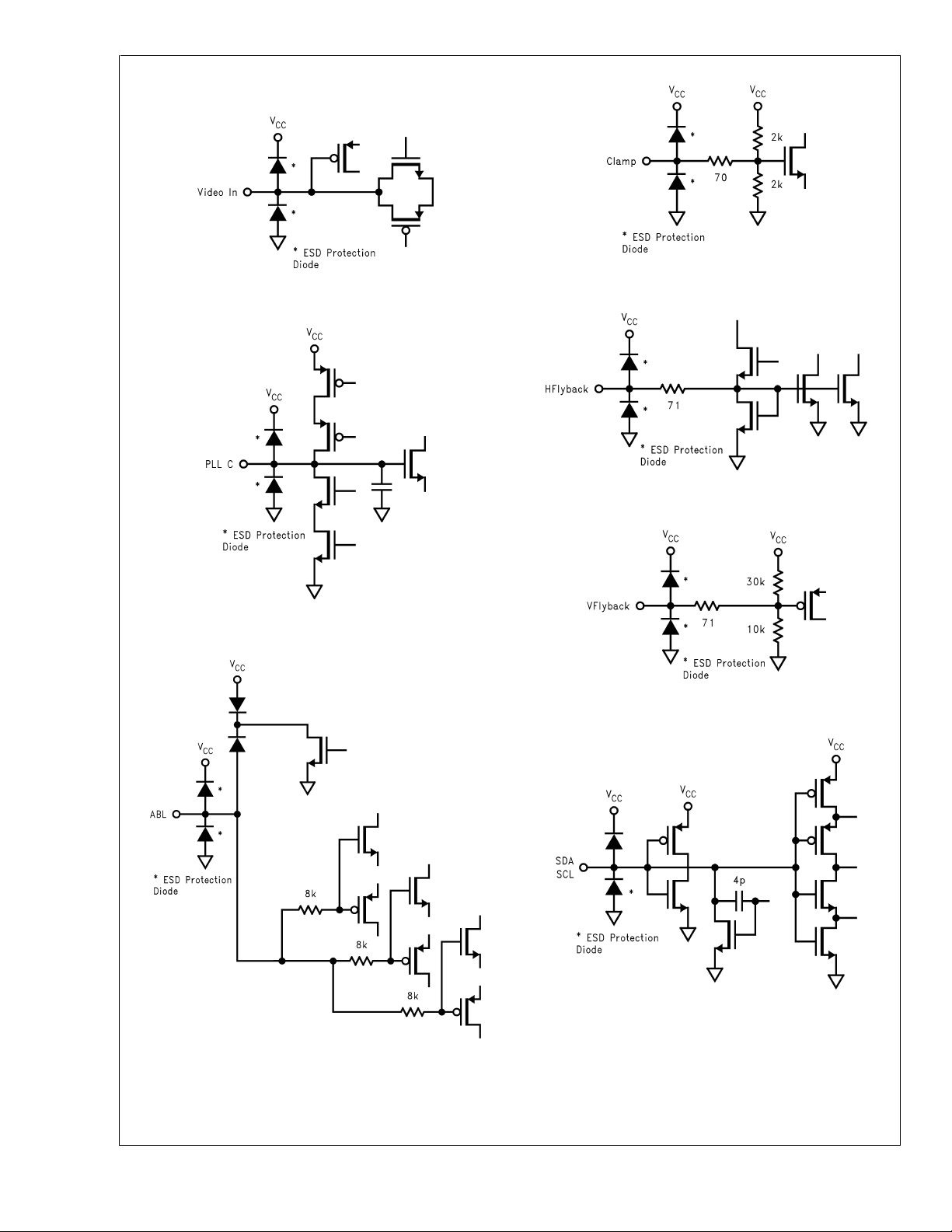
Pin 4, 5, 6 —Blue, Red, and Green Video In The red, blue,
and green video signal is AC coupled into these pins. The
value of the capacitors is very important as they also serve
Pin Descriptions (Continued)
as the DC clamp control capacitors. A value of 0.0047 µF is
used in the demo boards. The schematic shown in
which has a series resistance of 33Ω and clamp diodes to
V
and ground should be used to protect the LM1253A
CC
from ESD. A good ground should be between the input connector and the LM1253A. The video traces should be kept
short.
and 6,
Figure 29
Figure 14
shows the external schematic of pins 4, 5,
shows the internal schematic of pins 4, 5,
and 6.
Pin 7 — Analog Ground Ground for the video section of the
LM1253A. All ground pins of the LM1253A should be connected together by a ground plane under the LM1253A. See
Figure 31
, which shows a sample layout.
Pin 8 —Analog Supply 5V supply for the video section of
the preamp. A 0.1 µF capacitor should be connected between pin 7 and pin 8, as close as possible to the LM1253A.
A 100 µF capacitor should also be connected between pin 7
and pin 8.
Pin 9— Analog Supply 5V supply for the PLL section of the
LM1253A. A 0.1 µF capacitor should be connected between
pin 9 and pin 7, as close as possible to the LM1253A.
Pin 10—PLL Ground Ground for the PLL section of the
LM1253A. Only the PLL components connected to pin 11
should be connected to this ground pin. Pin 10 should also
be connected to the ground plane under the LM1253A. All
ground pins of the LM1253A should be connected together
by a ground plane under the LM1253A. See
shows a sample layout.
Pin 11—PLL C A resistor capacitor network is connected to
this pin. It is used to convert the charge current of the charge
pump of the PLL into a voltage that is used to control the
variable oscillator. These components should be located
very close to the LM1253A with a short ground trace to pin
10.
The recommended values are R28 = 6.2 kΩ, C23 = 0.1 µF,
and C33 = 2.2 nF. When these component values are used
the range and gain values in
Table 12
can be loaded into
register 843Eh.
Figure 29
Figure 31
, which
An example layout is shown in
the external schematic of pin 11,
Figure 31,Figure 29
Figure 15
shows the inter-
shows
nal schematic.
Pin 12—ABL The Auto Beam Limit control reduces the gain
of the video amplifiers in response to a control voltage proportional to the CRT beam current. The ABL acts on all three
channels in an identical manner.This is required for CRT life
and X-ray protection. The beam current limit circuit application is as shown in
Figure 7
: when no current is being drawn
by the EHT supply, current flows from the supply rail through
the ABL resistor and into the ABL input of the IC. The IC
clamps the input voltage to a low impedance voltage source
(the 5V supply rail).
When current is drawn from the EHT supply, the current
passes through the ABL resistor, and reduces the current
flowing into the ABL input of the IC.
When the EHT current is high enough, the current flowing
into the ABL input of the IC drops to zero. This current level
determines the ABL threshold and is given by:
Where:
V
is the external supply (usually the CRT driver supply rail,
S
about 80V)
V
R
I
is the threshold ABL voltage of the IC
ABL TH
is the ABL resistor value
ABL
is the ABL limit
ABL
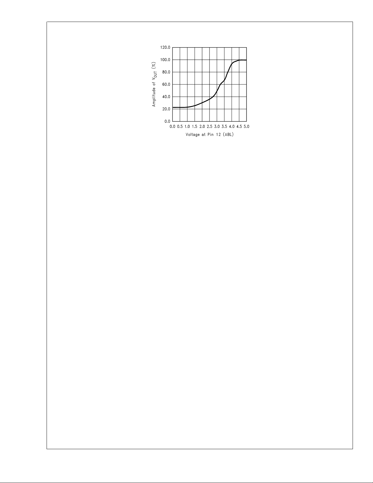
When the voltage on the ABL input drops below the ABL
threshold of the pre-amp, the gain of the pre-amp decreases,
which is shown in
Figure 8
, which reduces the beam current.
Afeedback loop is thus established which acts to prevent the
average beam current exceeding I
Figure 29
shows the external schematic of pin 12,
ABL
.
Figure 16
shows the internal schematic.
LM1253A
FIGURE 7. ABL
DS101265-12
www.national.com9
Pin Descriptions (Continued)
LM1253A
FIGURE 8. Effect of ABL Voltage on V
Pin 13—Clamp A positive going clamp signal is input on
this pin. Using this signal black level clamping of the video is
carried out directly on the input video that is AC coupled into
the high impedance preamplifier input, thus eliminating the
need for additional black level clamp capacitors.
shows the external schematic of pin 13,
internal schematic. An optional capacitor to ground may be
needed if noise interferes with the clamp signal.
Figure 17
Figure 29
shows the
DS101265-70
OUT
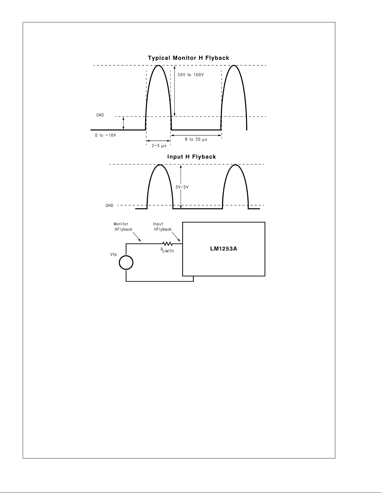
Pin 14—H Flyback H Flyback is an analog signal input from
the monitor horizontal scan. HBLANK is a digital signal derived from the horizontal flyback pulse as shown in
Figure 9
An optional capacitor and/or resistor to ground may be
needed if noise interferes with the H Flyback signal.
The horizontal flyback from the monitor must be a clean signal. There should be no ringing or other noise on the flyback.
.
www.national.com 10
Pin Descriptions (Continued)
LM1253A
FIGURE 9. H Flyback Input Pulse
R
is set to limit the input current into the IC to a maxi-
LIMITH
mum value of +1 mA during flyback and −150 µA during normal forward scan. For example if an h flyback with a peak of
100V is used, R
= 100 kΩ.The internal input imped-
LIMITH
ance of pin 14 is low to limit the maximum voltage swing at
the input to within the supply rail and ground. The IC interface circuit creates a digital signal from this waveform, which
is used as the blanking signal, and termed HBLANK. This
signal is used by the video amplifier for blanking the video
and by the OSD generator as the horizontal sync reference
for the PLL.
Loss of the horizontal flyback pulse implies that the monitor
is not scanning, and therefore no image is being displayed.
The HBLANK pulse is still required by the LM2453 CRT
driver in order to maintain correct bias conditions in the CRT
until the power supplies are switched off, but video will be set
at black level to prevent front of screen problems, using the
NO_VID line. See also the
Loss of Horizontal Flyback
sec-
tion.
Figure 29
shows the external schematic of pin 14,
Figure 18
shows the internal schematic.
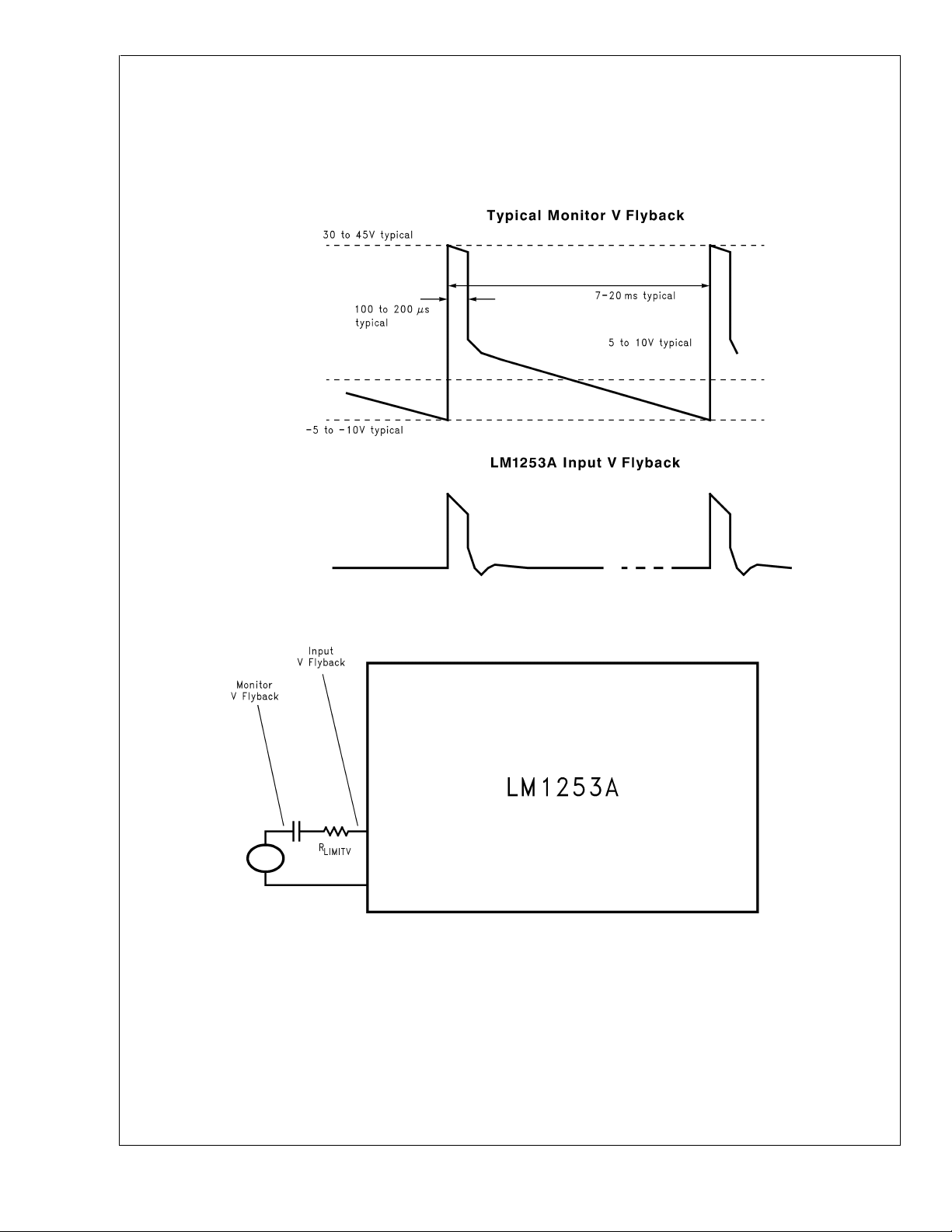
Pin 15—V Flyback This is an analog signal from the moni-
tor vertical scan. The analog waveform is AC coupled and
fed to the input of the IC via a current limiting resistor to pre-
DS101265-13
vent the positive and negative excursions of the signal causing excessive current or voltage swing at the input to the IC.
See
R
LIMITV
Figure 10
.
is set to limit the maximum input voltage swing into
the IC to less than the supply rails. The input to the IC is
positive edge triggered, and ignores the falling edge. Because of horizontal rate noise on the waveform, the input
buffer incorporates hysteresis, triggering at a positive going
threshold of V
and a negative going threshold of V
VTH+
VTH
The input buffer produces a digital signal VSTART which is
used to start the VBLANK timer. The positive rising edge of
VSTART sets a counter timer, which counts horizontal periods using the HBLANK signal. The timer resets VBLANK
when it reaches the value preset in the register VCOUNT
(set by the micro-controller over I
2
C). While the output
VBLANK is active, an AND function prevents any further
transitions on the VSTART waveform from retriggering the
counter.
The positive edge of the VSTART signal is initially transmitted through to VBLANK through an OR function, as the timer
may take up to one horizontal line period to begin timing the
duration of the pulse. The application must ensure that the
.
www.national.com11
Pin Descriptions (Continued)
VFLYBACKvertical flyback pulse is kept high during that ini-
LM1253A
tial period to prevent the output VBLANK from switching between high and low states.
Loss of vertical flyback pulse implies that the monitor is not
scanning, and therefore no image is being displayed. The
VBLANK pulses are still required by the LM2453 CRT driver
in order to maintain correct bias conditions in the CRT until
the power supplies are switched off, but video will be set at
black level to prevent front of screen problems, using the
NO_VID line. See also the
section.
Figure 19
Figure 29
shows the external schematic of pin 15,
shows the internal schematic.
Loss of Vertical Flyback Pulse
FIGURE 10. Vertical Flyback Input Pulse
Pin 16—SDA The I
2
C data line. A pull up resistor of about
2kΩshould be connected between this pin and +5V.A300Ω
resistor should be connected in series with the data line to
protect the IC against arcing.
schematic of pin 16,
Pin 17—SCL The I
Figure 20
2
C clock line. A pull up resistor of about
Figure 29
shows the external
shows the internal schematic.
2kΩshould be connected between this pin and +5V.A300Ω
resistor should be connected in series with the clock line to
protect the IC against arcing.
schematic of pin 17,
www.national.com 12
Figure 20
Figure 29
shows the external
shows the internal schematic.
DS101265-5
Pin 18 — Digital Ground Ground for the OSD section of the
LM1253A. All ground pins of the LM1253A should be connected together by a ground plane under the LM1253A. See
Figure 31
, which shows a sample layout.
Pin 19 —Digital Supply 5V supply for the OSD section of
the LM1253A. A 0.1 µF capacitor should be connected between pin 18 and pin 19, as close as possible to the
LM1253A.
LM1253A
Pin Descriptions (Continued)
Pin 20 —Digital Supply 5V supply for the OSD section of
the LM1253A. Pins 19 and 20 should be tied together under
normal operating conditions.
Pin 21—Analog Supply 5V supply for the video section of
the preamp. A 0.1 µF capacitor should be connected between pin 21 and pin 22, as close as possible to the
LM1253A.
Pin 22—Analog Ground Ground for the video section of
the LM1253A. All ground pins of the LM1253A should be
connected together by a ground plane under the LM1253A.
See
Figure 31
Pin 23, 24, and 25— Green, Red, and Blue Video Out
These pins output the red, green, and blue video information
in the VideoPlex format. These pins are connected to the
LM2453 using as short of traces as possible. An inductor
should be in series with the trace between the preamp and
CRT driver. The value of this inductor depends on the board
layout.
23, 24, and 25,
Pin 26—V
referenced to is output on this pin. A 0.1 µF capacitor should
be connected between this pin and ground and be located
close to the LM1253A. This pin is connected to the V
of the LM2453. A 0.1 µF capacitor also needs to be connected very close to the LM2453. A 100 µF capacitor should
also be connected to this trace.
ternal schematic of pin 26,
schematic.
Pin 27—Analog Ground Ground for the band gap reference section of the LM1253A. All ground pins of the
LM1253A should be connected together by a ground plane
under the LM1253A. See
layout.
Pin 28 — Analog Supply 5V supply for the band gap reference section of the preamp. A 0.1 µF capacitor should be
connected between pin 27 and pin 28, as close as possible
to the LM1253A. See
out.
, which shows a sample layout.
Figures 29, 30
REF
show the external schematic of pins
Figure 21
shows the internal schematic.
Out The voltage that the VideoPlex signal is
Figures 29, 30
Figure 31
Figure 31
Figure 22
, which shows a sample lay-
shows the internal
, which shows a sample
pin
REF
show the ex-
Input/Output Schematics
FIGURE 11. Pin 1 (R
FIGURE 12. Pin 2 (V Blank Out)
EXTVREF
DS101265-14
)
DS101265-15
FIGURE 13. Pin 3 (V
REF
DS101265-16
Cap)
www.national.com13
Input/Output Schematics (Continued)
LM1253A
DS101265-17
FIGURE 14. Pins 4, 5, and 6 (Video In)
DS101265-18
FIGURE 15. Pin 11 (PLL C)
DS101265-20
FIGURE 17. Pin 13 (Clamp)
DS101265-21
FIGURE 18. Pin 14 (H Flyback)
DS101265-22
FIGURE 19. Pin 15 (V Flyback)
DS101265-19
FIGURE 16. Pin 12 (ABL)
www.national.com 14
DS101265-23
FIGURE 20. Pins 16 and 17 (SDA and SCL)
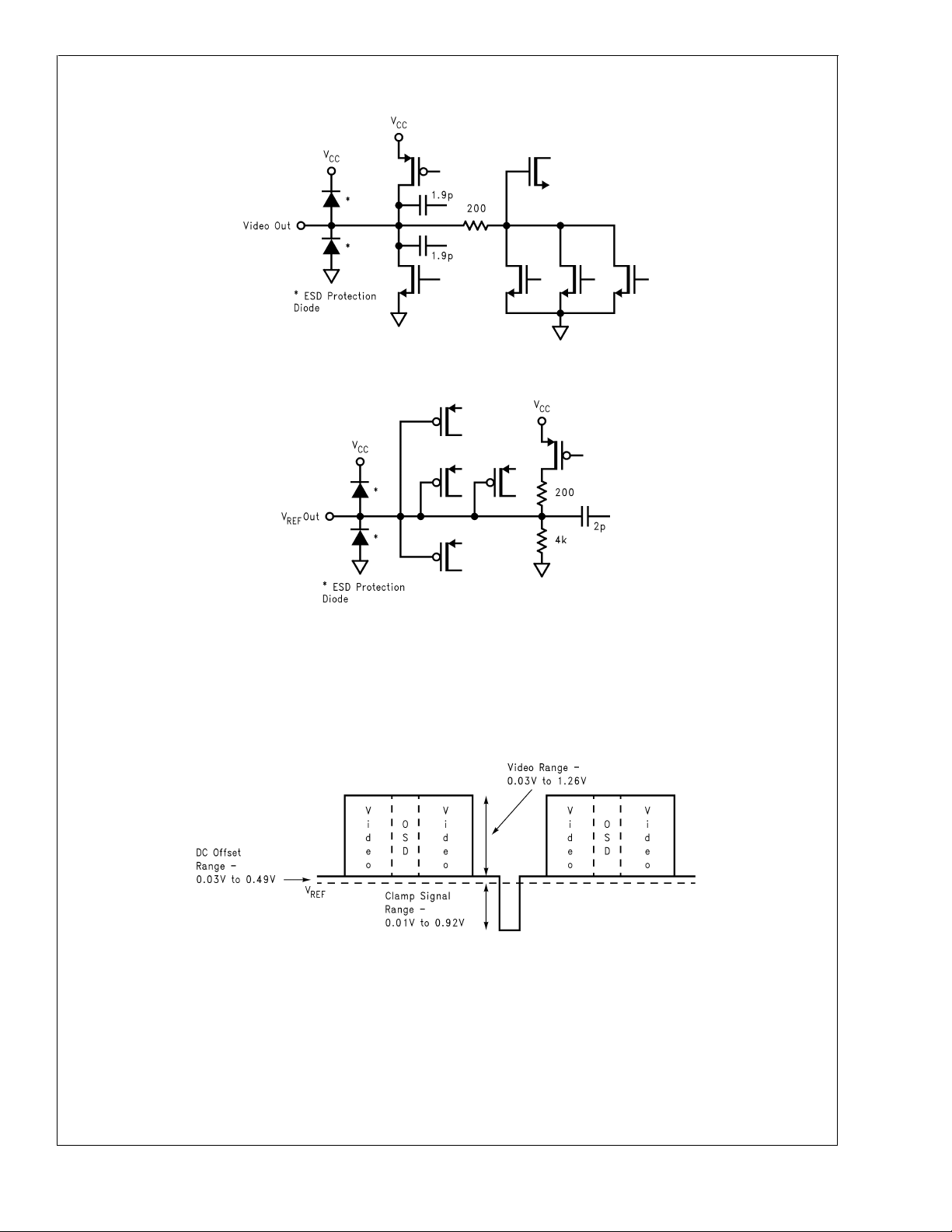
Input/Output Schematics (Continued)
FIGURE 21. Pins 23, 24, and 25 (Video Out)
LM1253A
DS101265-24
FIGURE 22. Pin 26 V
National VideoPlex Video System
The LM1253A CRT Pre-Amp in conjunction with the LM2453
CRT driver uses the National VideoPlex multiplexed video
FIGURE 23. National VideoPlex Video Signal (Pre-Amp Output)
The response of the LM2453 CRT driver to the VideoPlex
signal from the LM1253A Pre-Amp is shown in
Note that there are two sections in the video signal; the video
information is above V
and the clamp information is be-
REF
Figure 24
DS101265-25
Out
REF
signal to send the video signal and DC clamp level from the
pre-amp to the CRT driver. The basic signal scheme is
shown in
low V
.
LM2453 for an arbitrary video waveform from the LM1253A
is shown in
Figure 23
. The signals on the video out and clamp pins of the
REF
.
Figure 25
DS101265-26
.
www.national.com15
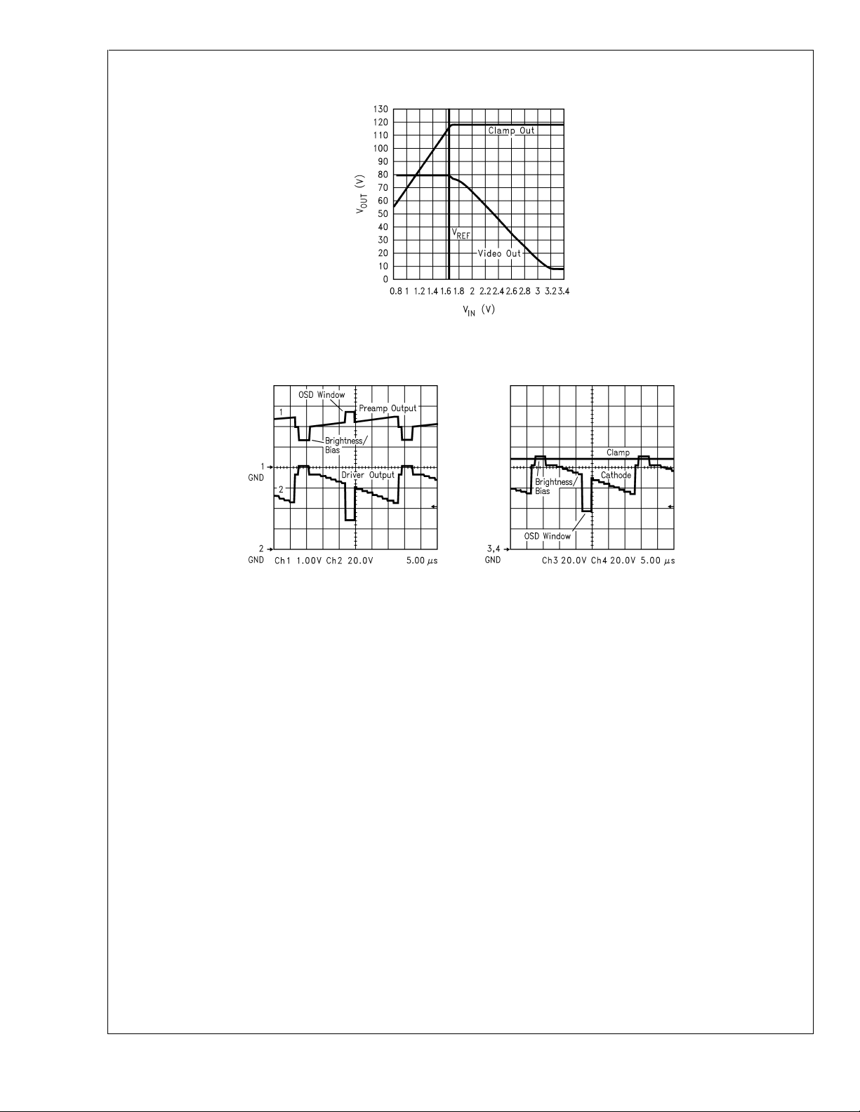
National VideoPlex Video System (Continued)
LM1253A
FIGURE 24. DC I/O Transfer Characteristics for the LM2453 CRT Driver
(Test Conditions: V
REF
= 1.65V, V
DS101265-27
= 80V, VBB= 8V)
CC1
FIGURE 25. LM2453 Input and Output Waveforms
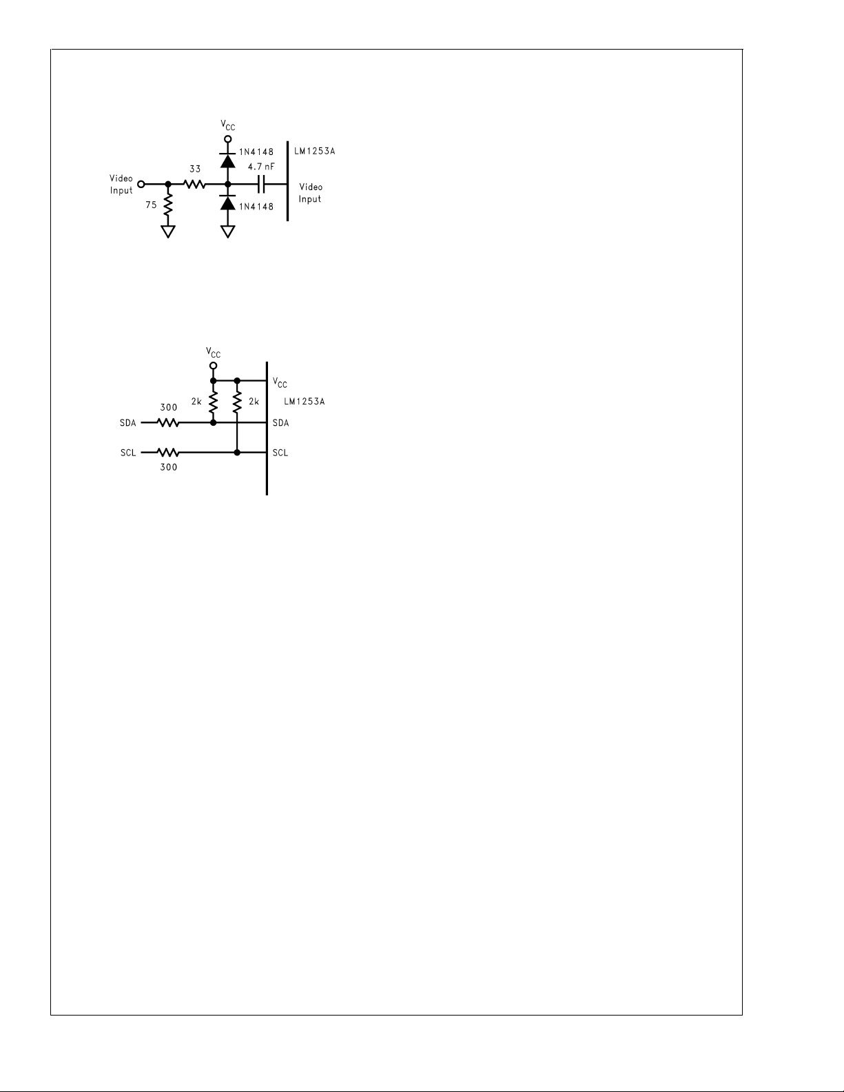
ESD and Arc-Over Protection
The LM1253A incorporates full ESD protection with special
consideration given to maximizing arc-over robustness. The
monitor designer must still use good circuit design and PCB
layout techniques. The human body model ESD susceptibility of the LM1253A is 2 kV,however many monitor manufacturers are now testing their monitors to the level 4 of the IEC
801-2 specification which requires the monitor to survive an
8 kV discharge. External ESD protection is needed to survive this level of ESD. The LM1253A provides excellent protection against both ESD and arc-over, but this is not a substitute for good PCB layout.
Figure 26
LM1253A. This provides the best protection against ESD.
When this protection is combined with good PCB layout the
LM1253A will easily survive the IEC 801-2 level 4 testing
(8 kV ESD). It is strongly recommended that the protection
diodes be added as shown in
has a maximum capacitance of 4 pF which will have little effect on the response of the video system due to the low impedance of the input video.
The ESD cells of the LM1253A also provide good protection
against arc-over, however good PCB layout is necessary.
The LM1253A should not be exposed directly to the voltages
that may occur during arc-over. The main vulnerability of the
LM1253A to arc-over is though the ground traces on the
PCB. For proper protection all ground connections associated with the LM1253A, including the grounds to the bypass
show the recommended input protection for the
Figure 26
. The 1N4148 diode
DS101265-28
capacitors, must have short returns to the ground pins. Asignificant ground plane should be used to connect all the
LM1253A grounds.
Figure 31
, which shows the demo board
layout, is an excellent example of an effective ground plane.
The list below should be followed to ensure a PCB with good
grounding:
All grounds associated with the LM1253A should be con-
•
nected together through a large ground plane.
CRT driver ground is connected to the video pre-amp
•
ground at one point.
CRTand arc protection grounds are connected directly to
•
the chassis or main ground. There is no arc-over current
flow from these grounds through the LM1253A grounds.
Input signal traces for SDA, SCL, H Flyback, V Flyback,
•
Clamp should be kept away from the LM2453 and all
traces that an arc can travel on.
Output signal traces of the LM1253A (video, V
•
V
) should be kept away from traces that carry the out-
REF
BLANK
put signals of the LM2453.
If any one of the above suggestions is not followed the
LM1253A may become more vulnerable to arc-over. Improper grounding is by far the most common cause of a
video pre-amp failure during arc-over.
,
www.national.com 16
LM1253A
ESD and Arc-Over Protection
(Continued)
DS101265-29
FIGURE 26. Recommended Video Input ESD Protection
2
The I
C specification recommends that the SDA and SCL
pins should be protected from arc-over.This is done by adding a resistor in series with each pin.
the resistors are connected to the SDA and SCL lines.
FIGURE 27. Recommended Arc-Over Protection for
SDA and SCL Pins
Figure 27
DS101265-30
shows how
Pre-Amp Functional Description
Figure 1
video signal is input to the LM1253A through the circuit
shown in
rectly on the AC coupled input signal at the input of the high
impedance buffer amplifier, thus eliminating the need for
black level clamp capacitors. The following sections then
modify the input video signal:
•
•
•
•
•
•
•
•
The above sections use the registers shown in
ure 28
signal each register controls.
shows the block diagram of the LM1253A. The
Figure 26
Contrast Attenuator—Sets the contrast level of the video
signal for all three channels.
Auto Beam Limit—Reduces the gain of all three video
amplifiers in response to a control voltage proportional to
the CRT beam current.
Gain Attenuator —Separately sets the gain for each
video channel.
Brightness—Sets the brightness for all three channels.
Bias—Adds an offset to the brightness controls for all
three video channels.
Pedestal—Adds a dc voltage offset to the brightness
control, in order that bi-directional control of the brightness control is always possible at all bias voltage settings.
Source Select—Switches between the input video signal
and the analog OSD signal generated by the 3 bit pallet
DAC control block.
DC Offset—Adds a dc voltage offset to all three video
outputs.
. Black level clamping is carried out di-
Table 2.Fig-
shows which section of the output video and clamp
www.national.com17
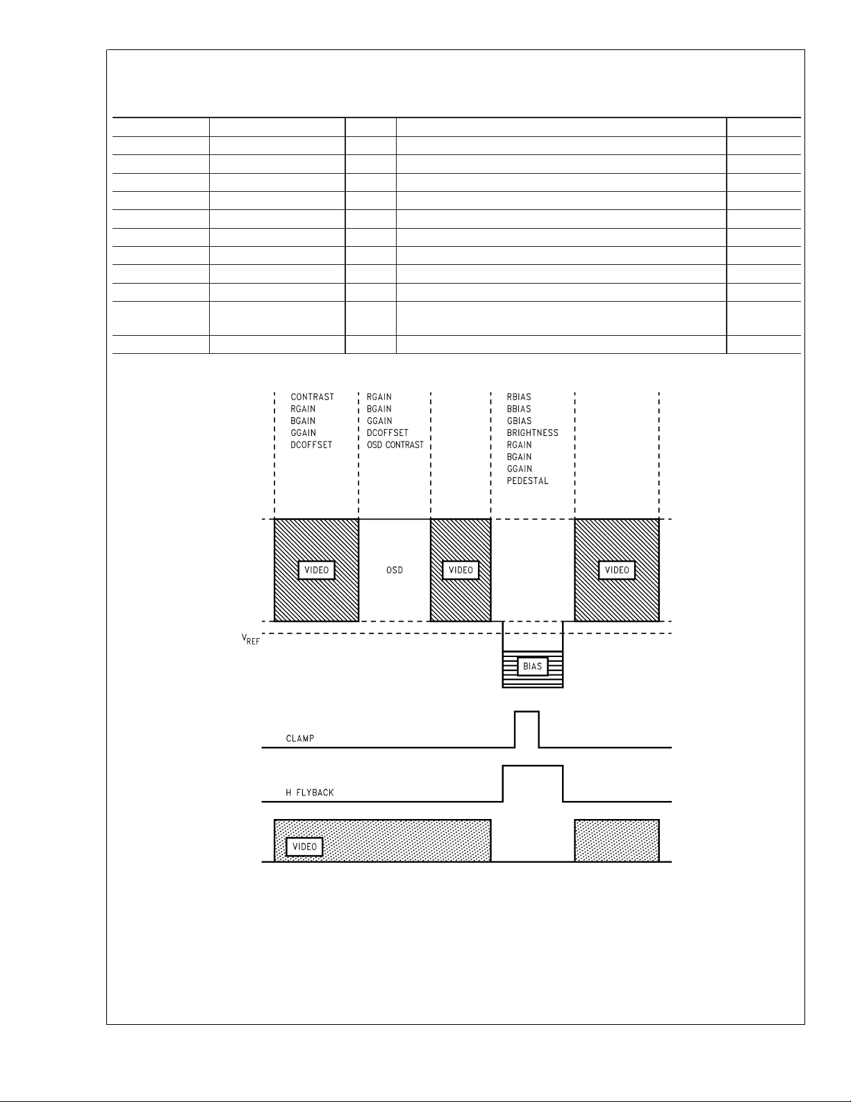
Pre-Amp Functional Description (Continued)
LM1253A
TABLE 2. Registers Controlling the Output Video and Clamp Signal
Parameter Address Size Description Default
BGAIN 8430h 7 Bit Blue Channel Gain 60h
GGAIN 8431h 7 Bit Green Channel Gain 60h
RGAIN 8432h 7 Bit Red Channel Gain 60h
CONTRAST 8433h 7 Bit Overall Gain of All Three Channels 60h
BBIAS 8434h 8 Bit Blue Bias Clamp Pulse Amplitude 80h
GBIAS 8435h 8 Bit Green Bias Clamp Pulse Amplitude 80h
RBIAS 8436h 8 Bit Red Bias Clamp Pulse Amplitude 80h
BRIGHTNESS 8437h 8 Bit Amplitude of Brightness Clamp Pulse of All 3 Channels 80h
PEDESTAL 8438h Bits 7–5 3 Bit Offset to the Brightness Control 4h
OSD
8438h Bits 4–3 2 Bit OSD Gain 2h
CONTRAST
DC OFFSET 8438h Bits 2–0 3 Bit Active Video DC Offset of All 3 Channels 4h
FIGURE 28. Register Control of the Output Video and Clamp Signal
An active horizontal blanking signal is added to the video at
the output, giving excellent smear performance, and preventing video content dependent DC bias offsets as a result
of high frequency over shoot.
www.national.com 18
DS101265-31
The outputs are referenced to a DC level (V
) produced by
REF
the LM1253A preamp, and so are guaranteed to provide
stable DC operating levels within the system without the
need for additional external feedback components.
 Loading...