

现货库存、技术资料、百科信息、热点资讯,精彩尽在鼎好!
LM124A/LM124QML
Low Power Quad Operational Amplifiers
LM124A/LM124QML Low Power Quad Operational Amplifiers
January 2005
General Description
The LM124/124A consists of four independent, high gain,
internally frequency compensated operational amplifiers
which were designed specifically to operate from a single
power supply over a wide range of voltages. Operation from
split power supplies is also possible and the low power
supply current drain is independent of the magnitude of the
power supply voltage.
Application areas include transducer amplifiers, DC gain
blocks and all the conventional op amp circuits which now
can be more easily implemented in single power supply
systems. For example, the LM124/124A can be directly operated off of the standard +5Vdc power supply voltage which
is used in digital systems and will easily provide the required
interface electronics without requiring the additional +15Vdc
power supplies.
Unique Characteristics
n In the linear mode the input common-mode voltage
range includes ground and the output voltage can also
swing to ground, even though operated from only a
single power supply voltage
n The unity gain cross frequency is temperature
compensated
n The input bias current is also temperature compensated
Advantages
n Eliminates need for dual supplies
n Four internally compensated op amps in a single
package
n Allows directly sensing near GND and V
to GND
n Compatible with all forms of logic
n Power drain suitable for battery operation
OUT
also goes
Features
n Internally frequency compensated for unity gain
n Large DC voltage gain 100 dB
n Wide bandwidth (unity gain) 1 MHz
(temperature compensated)
n Wide power supply range:
Single supply 3V to 32V
or dual supplies
n Very low supply current drain (700 µA) — essentially
independent of supply voltage
n Low input biasing current 45 nA
(temperature compensated)
n Low input offset voltage 2 mV
and offset current: 5 nA
n Input common-mode voltage range includes ground
n Differential input voltage range equal to the power
supply voltage
n Large output voltage swing 0V to V
±
1.5V to±16V
+
− 1.5V
Ordering Information
NS PART NUMBER SMD PART NUMBER NS PACKAGE NUMBER PACKAGE DISCRIPTION
LM124J/883 7704301CA J14A 14LD CERDIP
LM124AE/883 77043022A E20A 20LD LEADLESS CHIP CARRIER
LM124AJ/883 7704302CA J14A 14LD CERDIP
LM124AW/883 W14B 14LD CERPACK
LM124AWG/883 7704302XA WG14A 14LD CERAMIC SOIC
LM124AJLQMLV 5962L9950401VCA,
50k rd(Si)
LM124AJRQMLV 5962R9950401VCA,
100k rd(Si)
LM124AWGLQMLV 5962L9950401VZA,
50k rd(Si)
LM124AWGRQMLV 5962R9950401VZA,
100k rd(Si)
LM124AWLQMLV 5962L9950401VDA,
50k rd(Si)
LM124AWRQMLV 5962R9950401VDA,
100k rd(Si)
© 2005 National Semiconductor Corporation DS201080 www.national.com
J14A 14LD CERDIP
J14A 14LD CERDIP
WG14A 14LD CERAMIC SOIC
WG14A 14LD CERAMIC SOIC
W14B 14LD CERPACK
W14B 14LD CERPACK
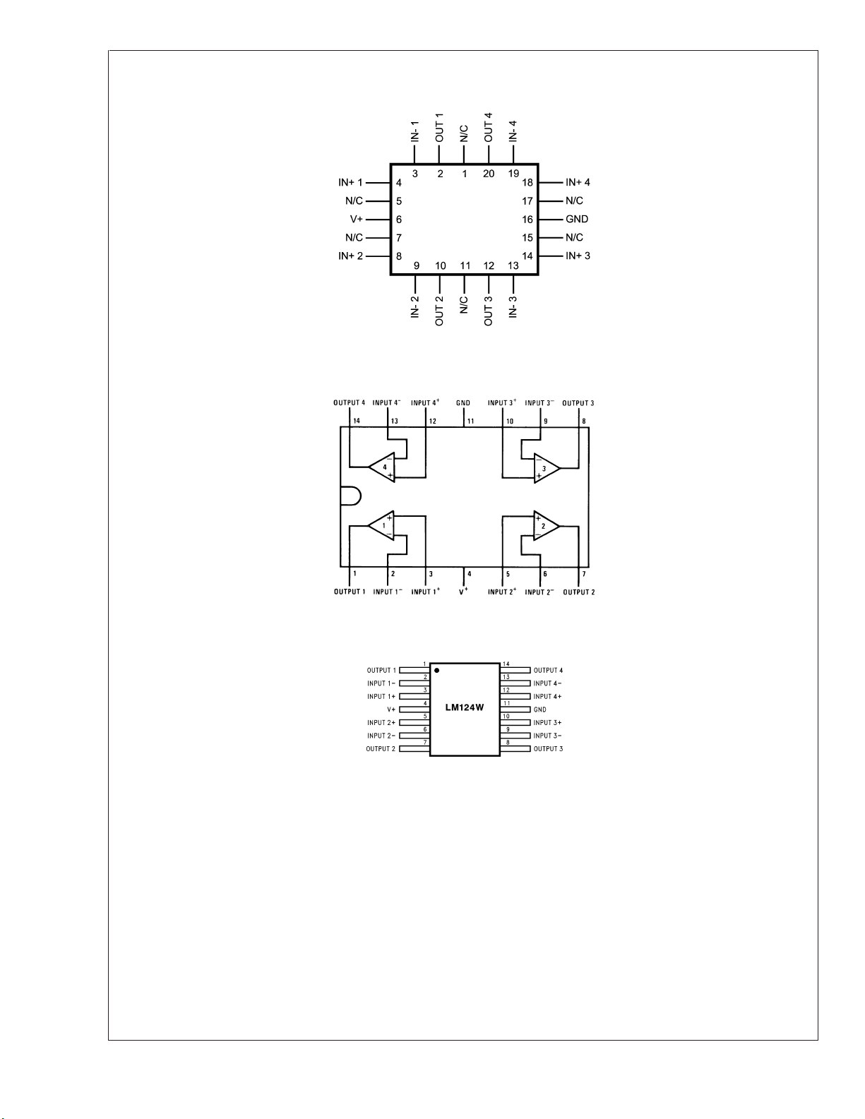
Connection Diagrams
LM124A/LM124QML
Leadless Chip Carrier
See NS Package Number E20A
Dual-In-Line Package
Top View
See NS Package Number J14A
20108055
20108001
See NS Package Number W14B or WG14A
www.national.com 2
20108033
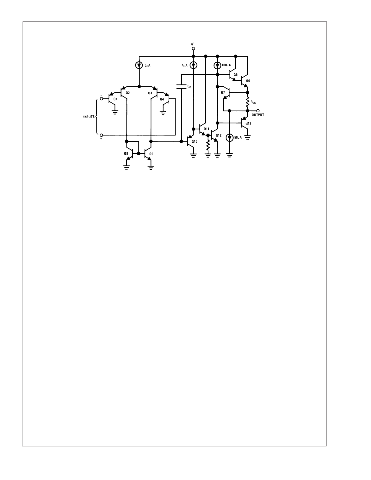
Schematic Diagram (Each Amplifier)
LM124A/LM124QML
20108002
www.national.com3

Absolute Maximum Ratings (Note 1)
If Military/Aerospace specified devices are required, please contact the National Semiconductor Sales Office/
Distributors for availability and specifications.
Supply Voltage, V
+
Differential Input Voltage 32Vdc
Input Voltage −0.3Vdc to +32Vdc
LM124A/LM124QML
Input Current
<
(V
−0.3Vdc) (Note 4) 50 mA
IN
Power Dissipation (Note 2)
CERDIP 1260mW
CERPACK 700mW
LCC 1350mW
CERAMIC SOIC 700mW
Output Short-Circuit to GND
(One Amplifier) (Note 3)
+
V
≤ 15Vdc and TA= 25˚C Continuous
Operating Temperature Range −55˚C ≤ T
Maximum Junction Temperature 150˚C
Storage Temperature Range −65˚C ≤ T
Lead Temperature (Soldering, 10 seconds) 260˚C
Thermal Resistance ThetaJA
CERDIP (Still Air) 103 C/W
(500LF/Min Air flow) 51 C/W
CERPACK (Still Air) 176 C/W
(500LF/Min Air flow) 116 C/W
LCC (Still Air) 91 C/W
(500LF/Min Air flow) 66 C/W
CERAMIC SOIC (Still Air) 176 C/W
(500LF/Min Air flow) 116 C/W
ThetaJC
CERDIP 19 C/W
CERPACK 18 C/W
LCC 24 C/W
CERAMIC SOIC 18 C/W
Package Weight (Typical)
CERDIP TBD
CERPACK TBD
LCC TBD
CERAMIC SOIC 410mg
ESD Tolerance (Note 5) 250V
Note 1: Absolute Maximum Ratings indicate limits beyond which damage to the device may occur. Operating Ratings indicate conditions for which the device is
functional, but do not guarantee specific performance limits. For guaranteed specifications and test conditions, see the Electrical Characteristics. The guaranteed
specifications apply only for the test conditions listed. Some performance characteristics may degrade when the device is not operated under the listed test
conditions.
Note 2: The maximum power dissipation must be derated at elevated temperatures and is dictated by Tjmax (maximum junction temperature), ThetaJA (package
junction to ambient thermal resistance), and TA (ambient temperature). The maximum allowable power dissipation at any temperature is Pdmax = (Tjmax TA)/ThetaJA or the number given in the Absolute Maximum Ratings, whichever is lower.
Note 3: Short circuits from the output to V+ can cause excessive heating and eventual destruction. When considering short circuits to ground, the maximum output
current is approximately 40mAindependent of the magnitude of V+. At values of supply voltage in excess of +15Vdc, continuous short-circuits can exceed the power
dissipation ratings and cause eventual destruction. Destructive dissipation can result from simultaneous shorts on all amplifiers.
Note 4: This input current will only exist when the voltage at any of the input leads is driven negative. It is due to the collector-base junction of the input PNP
transistors becoming forward biased and thereby acting as input diode clamps. In addition to this diode action, there is also lateral NPN parasitic transistor action
on the IC chip. This transistor action can cause the output voltages of the op amps to go to the V+ voltage level (or to ground for a large overdrive) for the time
duration that an input is driven negative. This is not destructive and normal output states will re-establish when the input voltage, which was negative, again returns
to a value greater than -0.3Vdc (at 25 C).
Note 5: Human body model, 1.5 kΩ in series with 100 pF.
32Vdc or +16Vdc
≤ +125˚C
A
≤ +150˚C
A
www.national.com 4
Quality Conformance Inspection
MIL-STD-883, Method 5005 — Group A
Subgroup Description Temp ( ˚C)
1 Static tests at +25
2 Static tests at +125
3 Static tests at -55
4 Dynamic tests at +25
5 Dynamic tests at +125
6 Dynamic tests at -55
7 Functional tests at +25
8A Functional tests at +125
8B Functional tests at -55
9 Switching tests at +25
10 Switching tests at +125
11 Switching tests at -55
LM124A/LM124QML
www.national.com5
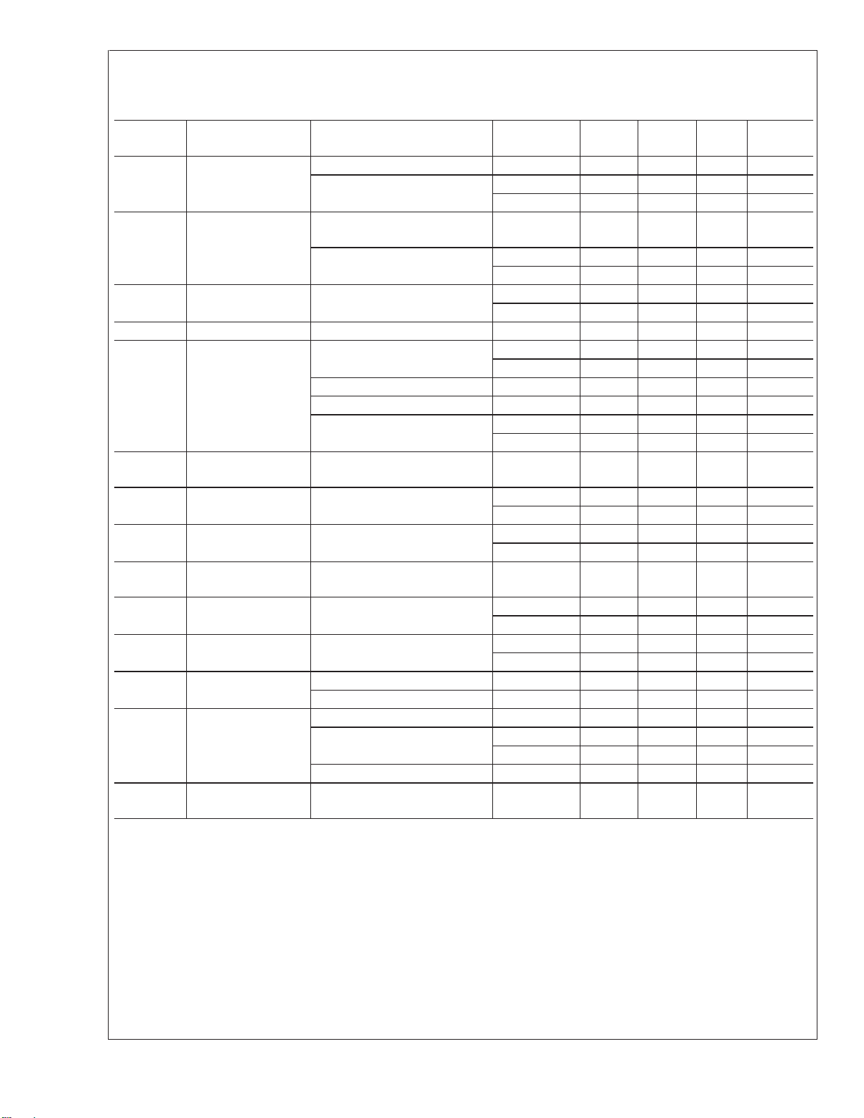
LM124A 883 DC Electrical Characteristics
(The following conditions apply to all the following parameters, unless otherwise specified.) All voltages referenced to device
ground.
SYMBOL PARAMETER CONDITIONS NOTES MIN MAX UNIT SUB-
Icc Power Supply Current V+ = 5V 1.2 mA 1, 2, 3
LM124A/LM124QML
Isink Output Sink Current V+ = 15V, Vout = 200mV,
Isource Output Source
Current
Ios Short Circuit Current V+ = 5V, Vout = 0V -60 mA 1
Vio Input Offset Voltage V+ = 30V, Vcm = 0V -2 2 mV 1
CMRR Common Mode
Rejection Ratio
±
Iib Input Bias Current V+ = 5V, Vcm = 0V -50 10 nA 1
Iio Input Offset Current V+ = 5V, Vcm = 0V -10 10 nA 1
PSRR Power Supply
Rejection Ratio
Vcm Common Mode
Voltage Range
Avs Large Signal Gain V+ = 15V, Rl = 2K Ohms,
Voh Output Voltage High V+ = 30V, Rl = 2K Ohms 26 V 4, 5, 6
Vol Output Voltage Low V+ = 30V, Rl = 10K Ohms 40 mV 4, 5, 6
Channel Separation
Amp to Amp Coupling
V+ = 30V 3.0 mA 1
4.0 mA 2, 3
12 uA 1
+Vin = 0mV, -Vin = +65mV
V+ = 15V, Vout = 2V,
+Vin = 0mV, -Vin = +65mV
V+ = 15V, Vout = 2V,
+Vin = 0mV, -Vin = -65mV
V+ = 30V, Vcm = 28.5V -2 2 mV 1
V+ = 30V, Vcm = 28V -4 4 mV 2, 3
V+ = 5V, Vcm = 0V -2 2 mV 1
V+ = 30V, Vin = 0V to 28.5V 70 dB 1
V+ = 5V to 30V, Vcm = 0V 65 dB 1
V+ = 30V (Note 6) 28.5 V 1
(Note 6) 28 V 2, 3
(Note 7) 50 V/mV 4
Vo=1Vto11V
V+ = 30V, Rl = 10K Ohms 27 V 4, 5, 6
V+ = 30V, Isink = 1uA 40 mV 4
V+ = 5V, Rl = 10K Ohms 20 mV 4, 5, 6
1KHz, 20KHz (Note 8) 80 dB 4
(Note 7) 25 V/mV 5, 6
10 mA 1
5mA2,3
-20 mA 1
-10 mA 2, 3
-4 4 mV 2, 3
-4 4 mV 2, 3
-100 10 nA 2, 3
-30 30 nA 2, 3
100 mV 5, 6
GROUPS
www.national.com 6
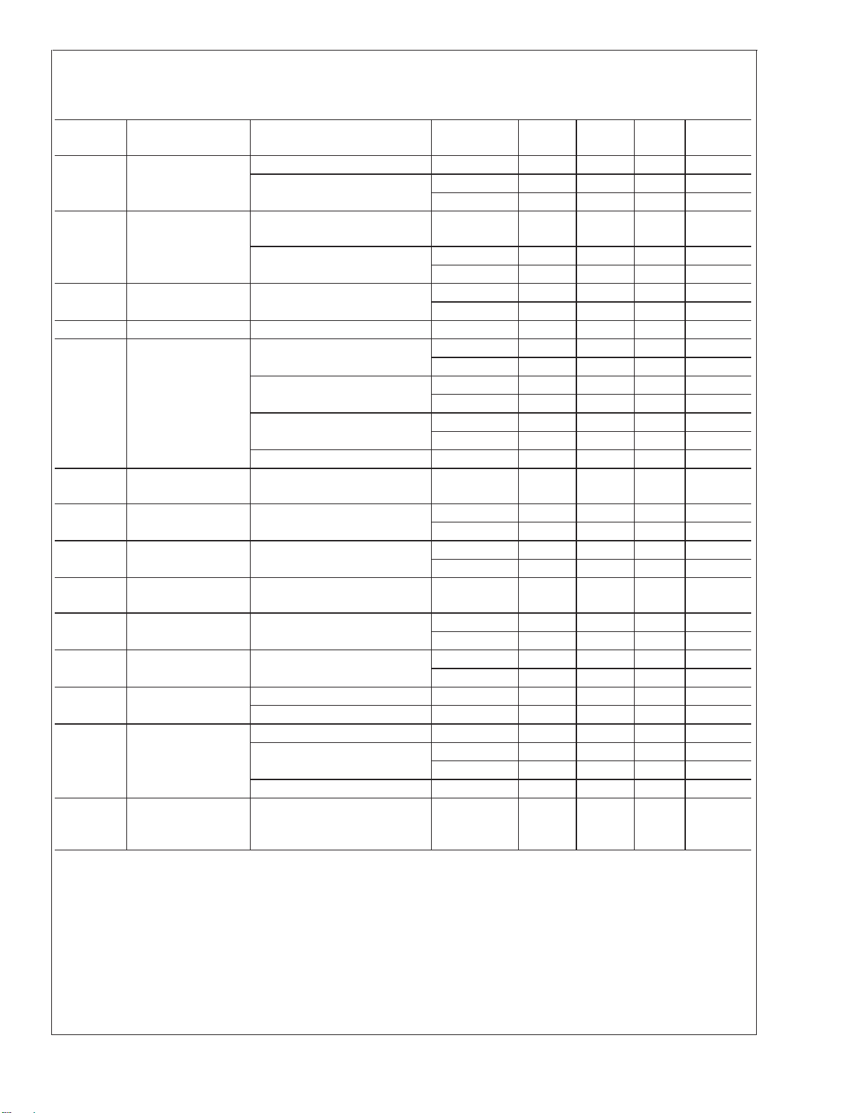
LM124 883 DC Electrical Characteristics
(The following conditions apply to all the following parameters, unless otherwise specified.) All voltages referenced to device
ground.
SYMBOL PARAMETER CONDITIONS NOTES MIN MAX UNIT SUB-
GROUPS
Icc Power Supply Current V+ = 5V 1.2 mA 1, 2, 3
V+ = 30V 3.0 mA 1
4.0 mA 2, 3
Isink Output Sink Current V+ = 15V, Vout = 200mV,
+Vin = 0mV, -Vin = +65mV
V+ = 15V, Vout = 2V,
+Vin = 0mV, -Vin = +65mV
Isource Output Source
Current
Ios Short Circuit Current V+ = 5V, Vout = 0V -60 mA 1
Vio Input Offset Voltage V+ = 30V, Vcm = 0V -5 5 mV 1
CMRR Common Mode
Rejection Ratio
+Iib Input Bias Current V+ = 5V, Vcm = 0V -150 10 nA 1
Iio Input Offset Current V+ = 5V, Vcm = 0V -30 30 nA 1
PSRR Power Supply
Rejection Ratio
Vcm Common Mode
Voltage Range
Avs Large Signal Gain V+ = 15V, Rl = 2K Ohms,
Voh Output Voltage High V+ = 30V, Rl = 2K Ohms 26 V 4, 5, 6
Vol Output Voltage Low V+ = 30V, Rl = 10K Ohms 40 mV 4, 5, 6
Channel Separation
(Amp to Amp
Coupling)
V+ = 15V, Vout = 2V,
+Vin = 0mV, -Vin = -65mV
V+ = 30V, Vcm = 28V -5 5 mV 1
V+ = 5V, Vcm = 0V -5 5 mV 1
V+ = 30V, Vcm = 28.5V -5 5 mV 1
V+ = 30V, Vin = 0V to 28.5V 70 dB 1
V+ = 5V to 30V, Vcm = 0V 65 dB 1
V+ = 30V (Note 6) 28.5 V 1
(Note 6) 28 V 2, 3
Vo=1Vto11V
V+ = 30V, Rl = 10K Ohms 27 V 4, 5, 6
V+ = 30V, Isink = 1uA 40 mV 4
V+ = 5V, Rl = 10K Ohms 20 mV 4, 5, 6
1KHz, 20KHz (Note 8) 80 dB 4
12 uA 1
10 mA 1
5mA2,3
-20 mA 1
-10 mA 2, 3
-7 7 mV 2, 3
-7 7 mV 2, 3
-7 7 mV 2, 3
-300 10 nA 2, 3
-100 100 nA 2, 3
50 V/mV 4
25 V/mV 5, 6
100 mV 5, 6
LM124A/LM124QML
www.national.com7
LM124A RAD HARD DC Electrical Characteristics (Note 10)
(The following conditions apply to all the following parameters, unless otherwise specified.) All voltages referenced to device
ground.
SYMBOL PARAMETER CONDITIONS NOTES MIN MAX UNIT SUB-
Vio Input Offset Voltage Vcc+ = 30V, Vcc- = Gnd,
LM124A/LM124QML
Iio Input Offset Current Vcc+ = 30V, Vcc- = Gnd,
±
Iib Input Bias Current Vcc+ = 30V, Vcc- = Gnd,
+PSRR Power Supply
Rejection Ratio
CMRR Common Mode
Rejection Ratio
Ios+ Output Short Circiut
Current
Icc Power Supply Current Vcc+ = 30V, Vcc- = Gnd 3 mA 1, 2
Delta Vio/
Delta T
Delta Iio/
Delta T
Input Offset Voltage
Temperature
Sensitivity
Input Offset Current
Temperature
Sensitivity
Vcm = -15V
Vcc+ = 2V, Vcc- = -28V,
Vcm = 13V
Vcc+ = 5V, Vcc- = Gnd,
Vcm = -1.4V
Vcc+ = 2.5V, Vcc- = -2.5,
Vcm = 1.1V
Vcm = -15V
Vcc+ = 2V, Vcc- = -28V,
Vcm = 13V
Vcc+ = 5V, Vcc- = Gnd,
Vcm = -1.4V
Vcc+ = 2.5V, Vcc- = -2.5,
Vcm = 1.1V
Vcm = -15V
Vcc+ = 2V, Vcc- = -28V,
Vcm = 13V
Vcc+ = 5V, Vcc- = Gnd,
Vcm = -1.4V
Vcc+ = 2.5V, Vcc- = -2.5,
Vcm = 1.1V
Vcc- = Gnd, Vcm = -1.4V,
5V ≤ Vcc ≤ 30V
Vcc+ = 30V, Vcc- = Gnd,
Vo = 25V
+25˚C ≤ TA ≤ +125˚C,
+Vcc = 5V, -Vcc = 0V,
Vcm = -1.4V
-55˚C ≤ TA ≤ +25˚C, +Vcc = 5V,
-Vcc = 0V, Vcm = -1.4V
+25˚C ≤ TA ≤ +125˚C,
+Vcc = 5V, -Vcc = 0V,
Vcm = -1.4V
-55˚C ≤ TA ≤ +25˚C, +Vcc = 5V,
-Vcc = 0V, Vcm = -1.4V
(Note 9) -30 30 uV/ ˚C 2
(Note 9) -30 30 uV/ ˚C 3
(Note 9) -400 400 pA/˚ C 2
(Note 9) -700 700 pA/ ˚C 3
-2 2 mV 1
-4 4 mV 2, 3
-2 2 mV 1
-4 4 mV 2, 3
-2 2 mV 1
-4 4 mV 2, 3
-2 2 mV 1
-4 4 mV 2, 3
-10 10 nA 1, 2
-30 30 nA 3
-10 10 nA 1, 2
-30 30 nA 3
-10 10 nA 1, 2
-30 30 nA 3
-10 10 nA 1, 2
-30 30 nA 3
-50 +0.1 nA 1, 2
-100 +0.1 nA 3
-50 +0.1 nA 1, 2
-100 +0.1 nA 3
-50 +0.1 nA 1, 2
-100 +0.1 nA 3
-50 +0.1 nA 1, 2
-100 +0.1 nA 3
-100 100 uV/V 1, 2, 3
76 dB 1, 2, 3
-70 mA 1, 2,3
4mA3
GROUPS
www.national.com 8
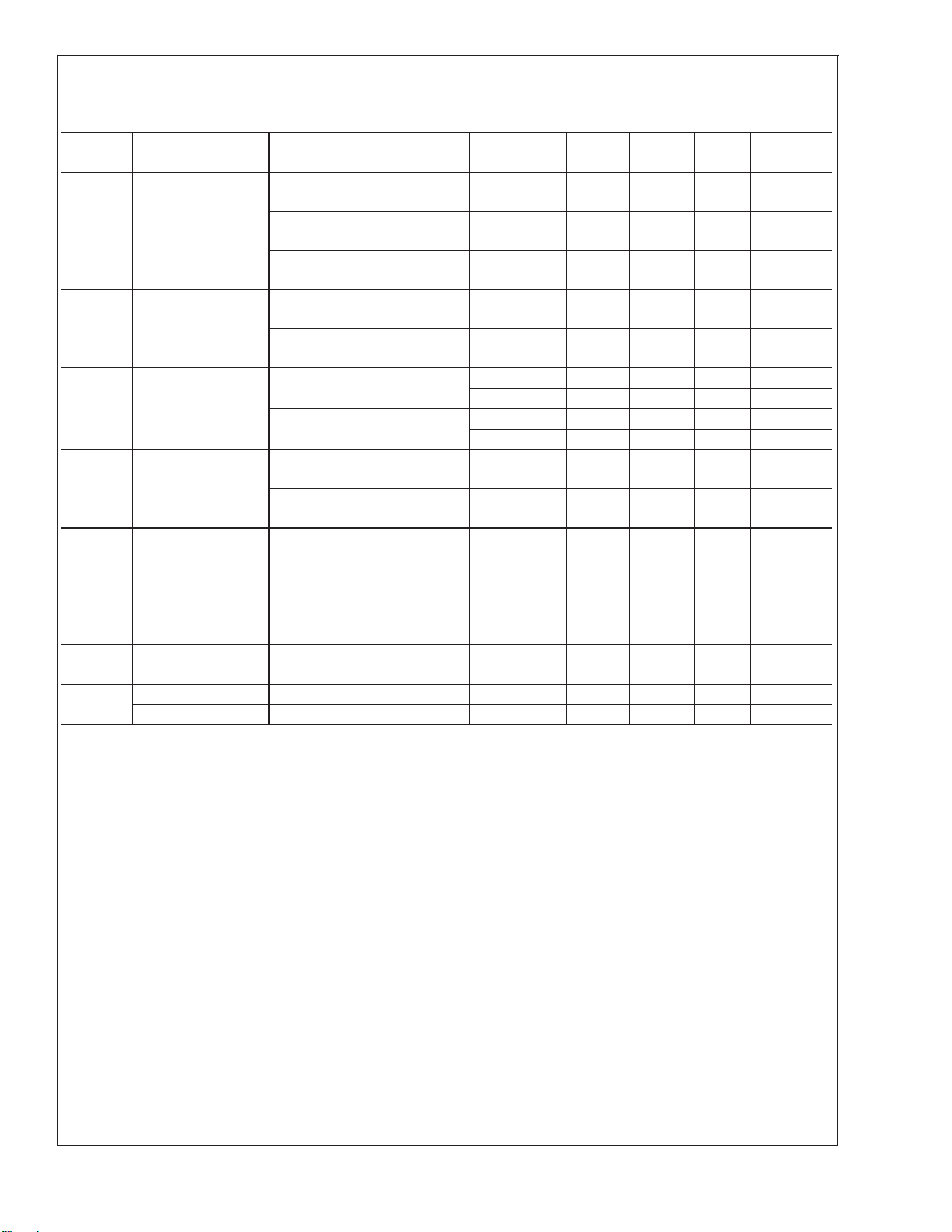
LM124A RAD HARD AC/DC Electrical Characteristics (Note 10)
(The following conditions apply to all the following parameters, unless otherwise specified.) All voltages referenced to device
ground.
SYMBOL PARAMETER CONDITIONS NOTES MIN MAX UNIT SUB-
GROUPS
Vol Logical "0" Output
Voltage
Voh Logical "1" Output
Voltage
Avs+ Voltage Gain
Avs Voltage Gain Vcc+ = 5V, Vcc- = Gnd,
+Vop Maximum Output
Voltage Swing
TR(tr) Transient Response:
Rise Time
TR(os) Transient Response:
Overshoot
±
Sr Slew Rate: Rise Vcc+ = 30V, Vcc- = Gnd 0.1 V/uS 7, 8A, 8B
Slew Rate: Fall Vcc+ = 30V, Vcc- = Gnd 0.1 V/uS 7, 8A, 8B
Vcc+ = 30V, Vcc- = Gnd,
Rl = 10K Ohms
Vcc+ = 30V, Vcc- = Gnd,
Iol = 5mA
Vcc+ = 4.5V, Vcc- = Gnd,
Iol = 2uA
Vcc+ = 30V, Vcc- = Gnd,
Ioh = -10mA
Vcc+ = 4.5V, Vcc- = Gnd,
Ioh = -10mA
Vcc+ = 30V, Vcc- = Gnd,
1V ≤ Vo ≤ 26V, Rl = 10K Ohms
Vcc+ = 30V, Vcc- = Gnd,
5V ≤ Vo ≤ 20V, Rl = 2K Ohms
1V ≤ Vo ≤ 2.5V, Rl = 10K Ohms
Vcc+ = 5V, Vcc- = Gnd,
1V ≤ Vo ≤ 2.5V, Rl = 2K Ohms
Vcc+ = 30V, Vcc- = Gnd,
Vo = +30V, Rl = 10K Ohms
Vcc+ = 30V, Vcc- = Gnd,
Vo = +30V, Rl = 2K Ohms
Vcc+ = 30V, Vcc- = Gnd 1 uS 7, 8A, 8B
Vcc+ = 30V, Vcc- = Gnd 50 % 7, 8A, 8B
27 V 4,5,6
2.4 V 4,5,6
50 V/mV 4
25 V/mV 5, 6
50 V/mV 4
25 V/mV 5, 6
10 V/mV 4, 5, 6
10 V/mV 4, 5, 6
27 V 4,5,6
26 V 4,5,6
35 mV 4, 5, 6
1.5 V 4,5,6
0.4 V 4,5,6
LM124A/LM124QML
www.national.com9

LM124A RAD HARD — AC Electrical Characteristics (Note 10)
(The following conditions apply to all the following parameters, unless otherwise specified.) AC: +Vcc = 30V, -Vcc = 0V
SYMBOL PARAMETER CONDITIONS NOTES MIN MAX UNIT SUB-
NI(BB) Noise Broadband +Vcc = 15V, -Vcc = -15V,
LM124A/LM124QML
NI(PC) Noise Popcorn +Vcc = 15V, -Vcc = -15V,
Cs Channel Separation +Vcc = 30V, -Vcc = Gnd,
BW = 10Hz to 5KHz
Rs = 20K Ohms,
BW = 10Hz to 5KHz
Rl = 2K Ohms
Rl = 2K Ohms,
Vin=1Vand16V,AtoB
Rl = 2K Ohms,
Vin=1Vand16V,AtoC
Rl = 2K Ohms,
Vin=1Vand16V,AtoD
Rl = 2K Ohms,
Vin=1Vand16V,BtoA
Rl = 2K Ohms,
Vin=1Vand16V,BtoC
Rl = 2K Ohms,
Vin=1Vand16V,BtoD
Rl = 2K Ohms,
Vin=1Vand16V,CtoA
Rl = 2K Ohms,
Vin=1Vand16V,CtoB
Rl = 2K Ohms,
Vin=1Vand16V,CtoD
Rl = 2K Ohms,
Vin=1Vand16V,DtoA
Rl = 2K Ohms,
Vin=1Vand16V,DtoB
Rl = 2K Ohms,
Vin=1Vand16V,DtoC
80 dB 7
80 dB 7
80 dB 7
80 dB 7
80 dB 7
80 dB 7
80 dB 7
80 dB 7
80 dB 7
80 dB 7
80 dB 7
80 dB 7
80 dB 7
15 uVrm s 7
50 uVpK 7
GROUPS
www.national.com 10

LM124A RAD HARD — DC Drift Values (Note 10)
(The following conditions apply to all the following parameters, unless otherwise specified.) DC: "Delta calculationsperformed
on QMLV devices at group B, subgroup 5 only"
SYMBOL PARAMETER CONDITIONS NOTES MIN MAX UNIT SUB-
GROUPS
Vio Input Offset Voltage Vcc+ = 30V, Vcc- = Gnd,
-0.5 0.5 mV 1
Vcm = -15V
±
Iib Input Bias Current Vcc+ = 30V, Vcc- = Gnd,
-10 10 nA 1
Vcm = -15V
Electrical Characteristics — POST RADIATION LIMITS +25˚C (Note 10)
(The following conditions apply to all the following parameters, unless otherwise specified.) All voltages referenced to device
ground.
SYMBOL PARAMETER CONDITIONS NOTES MIN MAX UNIT SUB-
GROUPS
Vio Input Offset Voltage Vcc+ = 30V, Vcc- = Gnd,
Vcm = -15V
Vcc+ = 2V, Vcc- = -28V,
Vcm = 13V
Vcc+ = 5V, Vcc- = GND,
Vcm = -1.4V
Vcc+ = 2.5V, Vcc- = -2.5,
Vcm = 1.1V
Iio Input Offset Current Vcc+ = 30V, Vcc- = GND,
Vcm = -15V
Vcc+ = 2V, Vcc- = -28V,
Vcm = 13V
Vcc+ = 5V, Vcc- = GND,
Vcm = -1.4V
Vcc+ = 2.5V, Vcc- = -2.5V,
Vcm = 1.1V
±
Iib Input Bias Current Vcc+ = 30V, Vcc- = GND,
Vcm = -15V
Vcc+ = 2V, Vcc- = -28V,
Vcm = 13V
Vcc+ = 5V, Vcc- = GND,
Vcm = -1.4V
Vcc+ = 2.5V, Vcc- = -2.5V,
Vcm = 1.1V
Avs+ Voltage Gain Vcc+ = 30V, Vcc- = GND,
1V ≤ Vo ≤ 26V, Rl = 10K Ohms
Vcc+ = 30V, Vcc- = GND,
5V ≤ Vo ≤ 20V, Rl = 2K Ohms
Note 6: Guaranteed by Vio tests.
Note 7: Datalog reading in K=V/mV
Note 8: Guaranteed, not tested
Note 9: Calculated parameters
Note 10: Pre and post irradiation limits are identical to those listed under AC and DC electrical characteristics except as listed in the Post Radiation Limits Table.
These parts may be dose rate sensitive in a space environment and demonstrate enhanced low dose rate effect. Radiation end point limits for the noted parameters
are guaranteed only for the conditions as specified in MIL-STD-883, Method 1019
(Note 10) -2.5 2.5 mV 1
(Note 10) -2.5 2.5 mV 1
(Note 10) -2.5 2.5 mV 1
(Note 10) -2.5 2.5 mV 1
(Note 10) -15 15 nA 1
(Note 10) -15 15 nA 1
(Note 10) -15 15 nA 1
(Note 10) -15 15 nA 1
(Note 10) -75 +0.1 nA 1
(Note 10) -75 +0.1 nA 1
(Note 10) -75 +0.1 nA 1
(Note 10) -75 +0.1 nA 1
(Note 10) 40 V/mV 4
(Note 10) 40 V/mV 4
LM124A/LM124QML
www.national.com11

Typical Performance Characteristics
Input Voltage Range Input Current
LM124A/LM124QML
20108034 20108035
Supply Current Voltage Gain
Open Loop Frequency
Response
20108036 20108037
Common Mode Rejection
Ratio
20108038
20108039
www.national.com 12

Typical Performance Characteristics (Continued)
LM124A/LM124QML
Voltage Follower Pulse
Response
Large Signal Frequency
Response
20108040
Voltage Follower Pulse
Response (Small Signal)
20108041
Output Characteristics
Current Sourcing
20108042
Output Characteristics
Current Sinking Current Limiting
20108044
20108043
20108045
www.national.com13

Application Hints
The LM124 series are op amps which operate with only a
single power supply voltage, have true-differential inputs,
and remain in the linear mode with an input common-mode
voltage of 0 V
of power supply voltage with little change in performance
characteristics. At 25˚C amplifier operation is possible down
to a minimum supply voltage of 2.3 V
LM124A/LM124QML
The pinouts of the package have been designed to simplify
PC board layouts. Inverting inputs are adjacent to outputs for
all of the amplifiers and the outputs have also been placed at
the corners of the package (pins 1, 7, 8, and 14).
Precautions should be taken to insure that the power supply
for the integrated circuit never becomes reversed in polarity
or that the unit is not inadvertently installed backwards in a
test socket as an unlimited current surge through the resulting forward diode within the IC could cause fusing of the
internal conductors and result in a destroyed unit.
Large differential input voltages can be easily accommodated and, as input differential voltage protection diodes are
not needed, no large input currents result from large differential input voltages. The differential input voltage may be
larger than V
should be provided to prevent the input voltages from going
negative more than −0.3 V
with a resistor to the IC input terminal can be used.
To reduce the power supply drain, the amplifiers have a
class A output stage for small signal levels which converts to
class B in a large signal mode. This allows the amplifiers to
both source and sink large output currents. Therefore both
NPN and PNP external current boost transistors can be used
to extend the power capability of the basic amplifiers. The
output voltage needs to raise approximately 1 diode drop
above ground to bias the on-chip vertical PNP transistor for
output current sinking applications.
For ac applications, where the load is capacitively coupled to
the output of the amplifier, a resistor should be used, from
the output of the amplifier to ground to increase the class A
bias current and prevent crossover distortion.
. These amplifiers operate over a wide range
DC
.
DC
+
without damaging the device. Protection
(at 25˚C). An input clamp diode
DC
Where the load is directly coupled, as in dc applications,
there is no crossover distortion.
Capacitive loads which are applied directly to the output of
the amplifier reduce the loop stability margin. Values of
50 pF can be accommodated using the worst-case noninverting unity gain connection. Large closed loop gains or
resistive isolation should be used if larger load capacitance
must be driven by the amplifier.
The bias network of the LM124 establishes a drain current
which is independent of the magnitude of the power supply
voltage over the range of from 3 V
to 30 VDC.
DC
Output short circuits either to ground or to the positive power
supply should be of short time duration. Units can be destroyed, not as a result of the short circuit current causing
metal fusing, but rather due to the large increase in IC chip
dissipation which will cause eventual failure due to excessive junction temperatures. Putting direct short-circuits on
more than one amplifier at a time will increase the total IC
power dissipation to destructive levels, if not properly protected with external dissipation limiting resistors in series
with the output leads of the amplifiers. The larger value of
output source current which is available at 25˚C provides a
larger output current capability at elevated temperatures
(see typical performance characteristics) than a standard IC
op amp.
The circuits presented in the section on typical applications
emphasize operation on only a single power supply voltage.
If complementary power supplies are available, all of the
standard op amp circuits can be used. In general, introducing a pseudo-ground (a bias voltage reference of V
+
/2) will
allow operation above and below this value in single power
supply systems. Many application circuits are shown which
take advantage of the wide input common-mode voltage
range which includes ground. In most cases, input biasing is
not required and input voltages which range to ground can
easily be accommodated.
www.national.com 14

Typical Single-Supply Applications
(V+= 5.0 VDC)
Non-Inverting DC Gain (0V Input = 0V Output)
LM124A/LM124QML
*R not needed due to temperature independent I
DC Summing Amplifier
≥ 0VDCand VO≥ VDC) Power Amplifier
(V
IN’S
Where: V0=V1+V2−V3−V
(V1+V2) ≥ (V3+V4) to keep V
4
>
0V
O
IN
20108006
DC
V0=0VDCfor VIN=0V
AV=10
DC
20108005
20108007
www.national.com15

Typical Single-Supply Applications (V
LED Driver “BI-QUAD” RC Active Bandpass Filter
LM124A/LM124QML
20108008
+
= 5.0 VDC) (Continued)
fo= 1 kHz
Q=50
= 100 (40 dB)
A
V
Fixed Current Sources Lamp Driver
20108010
20108009
20108011
www.national.com 16

LM124A/LM124QML
Typical Single-Supply Applications
(V+= 5.0 VDC) (Continued)
Current Monitor
20108012
Pulse Generator
20108015
Squarewave Oscillator
*(Increase R1 for ILsmall)
Driving TTL
20108016
Pulse Generator
20108013
Voltage Follower
20108014
20108017
www.national.com17

Typical Single-Supply Applications (V
High Compliance Current Sink
LM124A/LM124QML
+
= 5.0 VDC) (Continued)
IO= 1 amp/volt V
(Increase REfor Iosmall)
IN
20108018
Low Drift Peak Detector
www.national.com 18
20108019

Typical Single-Supply Applications (V
Comparator with Hysteresis Ground Referencing a Differential Input Signal
20108020
+
= 5.0 VDC) (Continued)
LM124A/LM124QML
Voltage Controlled Oscillator Circuit
*Wide control voltage range: 0 VDC≤ VC≤ 2(V+−1.5 VDC)
VO=V
R
Photo Voltaic-Cell Amplifier
20108021
20108022
20108023
www.national.com19

Typical Single-Supply Applications (V
AC Coupled Inverting Amplifier
LM124A/LM124QML
AC Coupled Non-Inverting Amplifier
+
= 5.0 VDC) (Continued)
20108024
www.national.com 20
20108025

Typical Single-Supply Applications (V
DC Coupled Low-Pass RC Active Filter
+
= 5.0 VDC) (Continued)
LM124A/LM124QML
fO= 1 kHz
Q=1
=2
A
V
20108026
High Input Z, DC Differential Amplifier
20108027
www.national.com21

Typical Single-Supply Applications (V
DC Instrumentation Amplifier
LM124A/LM124QML
+
= 5.0 VDC) (Continued)
High Input Z Adjustable-Gain
20108028
Using Symmetrical Amplifiers to
Reduce Input Current (General Concept)
Bridge Current Amplifier
20108030
20108029
www.national.com 22

Typical Single-Supply Applications (V
Bandpass Active Filter
+
= 5.0 VDC) (Continued)
LM124A/LM124QML
fO= 1 kHz
Q=25
20108031
www.national.com23

Revision History Section
Date
Released Revision Section Originator Changes
9–2–04 A New Release, Corporate format R. Malone 3 MDS data sheets converted into one
Corp. data sheet format. MNLM124-X,
LM124A/LM124QML
01/27/05 B Connection Diagrams, Quality
Conformance Inspection Section,
and Physical Dimensions drawings
R. Malone Added E package Connection Diagram.
Rev. 1A2, MNLM124A-X, Rev. 1A3 and
MRLM124A-X-RH, Rev. 5A0. MDS data
sheets will be archived.
Changed verbiage under Quality
Conformance Title, and Updated
Revisions for the Marketing Drawings.
www.national.com 24

Physical Dimensions inches (millimeters) unless otherwise noted
SAMPLE TEXT Ceramic Dual-In-Line Package (J)
NS Package Number J14A
LM124A/LM124QML
SAMPLE TEXT 20 Pin Leadless Chip Carrier, Type C (E)
NS Package Number E20A
www.national.com25

Physical Dimensions inches (millimeters) unless otherwise noted (Continued)
LM124A/LM124QML
SAMPLE TEXT Ceramic Flatpak Package
NS Package Number W14B
SAMPLE TEXT 14-Pin Ceramic Package (WG)
NS Package Number WG14A
www.national.com 26

Notes
LM124A/LM124QML Low Power Quad Operational Amplifiers
National does not assume any responsibility for use of any circuitry described, no circuit patent licenses are implied and National reserves
the right at any time without notice to change said circuitry and specifications.
For the most current product information visit us at www.national.com.
LIFE SUPPORT POLICY
NATIONAL’S PRODUCTS ARE NOT AUTHORIZED FOR USE AS CRITICAL COMPONENTS IN LIFE SUPPORT DEVICES OR SYSTEMS
WITHOUT THE EXPRESS WRITTEN APPROVAL OF THE PRESIDENT AND GENERAL COUNSEL OF NATIONAL SEMICONDUCTOR
CORPORATION. As used herein:
1. Life support devices or systems are devices or systems
which, (a) are intended for surgical implant into the body, or
(b) support or sustain life, and whose failure to perform when
properly used in accordance with instructions for use
2. A critical component is any component of a life support
device or system whose failure to perform can be reasonably
expected to cause the failure of the life support device or
system, or to affect its safety or effectiveness.
provided in the labeling, can be reasonably expected to result
in a significant injury to the user.
BANNED SUBSTANCE COMPLIANCE
National Semiconductor certifies that the products and packing materials meet the provisions of the Customer Products Stewardship
Specification (CSP-9-111C2) and the Banned Substances and Materials of Interest Specification (CSP-9-111S2) and contain no ‘‘Banned
Substances’’ as defined in CSP-9-111S2.
National Semiconductor
Americas Customer
Support Center
Email: new.feedback@nsc.com
Tel: 1-800-272-9959
www.national.com
National Semiconductor
Europe Customer Support Center
Fax: +49 (0) 180-530 85 86
Email: europe.support@nsc.com
Deutsch Tel: +49 (0) 69 9508 6208
English Tel: +44 (0) 870 24 0 2171
Français Tel: +33 (0) 1 41 91 8790
National Semiconductor
Asia Pacific Customer
Support Center
Email: ap.support@nsc.com
National Semiconductor
Japan Customer Support Center
Fax: 81-3-5639-7507
Email: jpn.feedback@nsc.com
Tel: 81-3-5639-7560
 Loading...