


November 2003
LM1246
150 MHz I
2
C Compatible RGB Preamplifier with Internal
512 Character OSD ROM, 512 Character RAM and 4
DACs
General Description
The LM1246 pre-amp is an integrated CMOS CRT preamp.
It has an I
the parameters necessary to directly setup and adjust the
gain and contrast in the CRT display. Brightness and bias
can be controlled through the DAC outputs, which are well
matched to the LM2479 and LM2480 integrated bias clamp
ICs. The LM1246 preamp is also designed to be compatible
with the LM246x high gain driver family.
Black level clamping of the video signal is carried out directly
on the AC coupled input signal into the high impedance
preamplifier input, thus eliminating the need for additional
clamp capacitors. Horizontal and vertical blanking of the
outputs is provided. Vertical blanking is optional and its
duration is register programmable.
The IC is packaged in an industry standard 24-lead DIP
molded plastic package.
2
C compatible interface which allows control of all
Features
n Fully addressable 512 Character OSD, simiilar in
features to the LM1237/LM1247, with selectable 2
byte character addressing or LM1247 bank select
modes
n Internal 512 character OSD ROM usable as either (a)
384 2-color plus 128 4-color characters, (b) 640 2-color
characters, or (c) some combination in between
n Internal 512 character RAM, which can be displayed as
one single or two independent windows
n Enhanced I
to allow versatile Page RAM access
2
C compatible microcontroller interface
n OSD Window Fade In/Fade Out
n OSD Half Tone Transparency
n Video Data dectection for Auto Centering & Sizing
n OSD override allows OSD messages to override video
and the use of burn-in screens with no video output.
n 4 DAC outputs (8-bit resolution) for bus controlled CRT
bias and brightness
n Spot killer which blanks the video outputs when V
falls below the specified threshold
n Suitable for use with discrete or integrated clamp, with
software configurable brightness mixer
n 4-Bit Programmable start position for internal
Horizontal Blanking
n Horizontal blanking and OSD synchronization directly
from deflection signals. The blanking can be disabled, if
desired.
n Vertical blanking and OSD synchronization directly from
deflection signals. The blanking width is register
programmable and can be disabled, if desired.
n Power Saving Mode with 65% power reduction
n Matched to LM246x driver and LM2479/80 bias IC’s
Applications
n Low end 15" and 17" bus controlled monitors with OSD
n 1024x768 displays up to 85 Hz requiring OSD capability
n Very low cost systems with LM246x driver
Character RAM and 4 DACs
LM1246 150 MHz I
2
C Compatible RGB Preamplifier with Internal 512 Character OSD ROM, 512
CC
© 2003 National Semiconductor Corporation DS200685 www.national.com
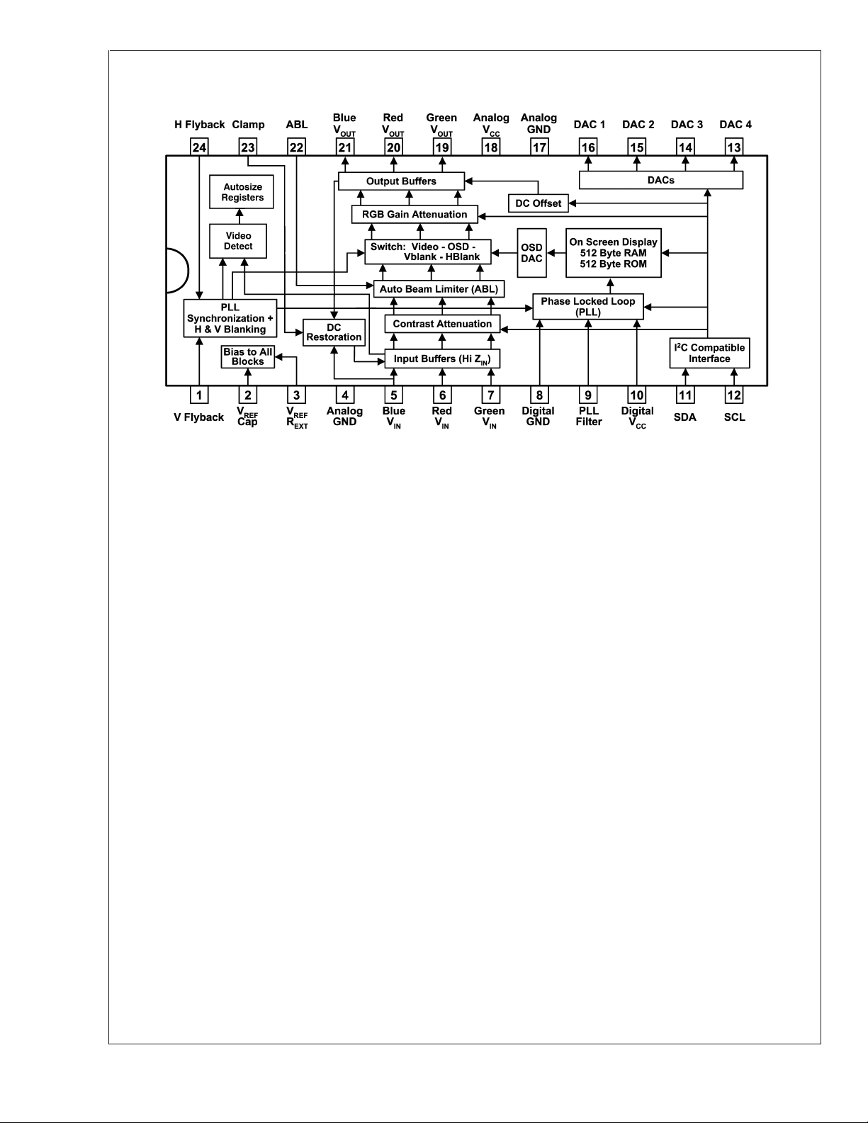
Internal Block Diagram
LM1246
20068501
FIGURE 1. Order Number LM1246AAA/NA
See NS Package Number N24D
www.national.com 2

LM1246
Absolute Maximum Ratings (Notes 1,
3)
If Military/Aerospace specified devices are required,
please contact the National Semiconductor Sales Office/
Distributors for availability and specifications.
Supply Voltage V
, Pins 10 and 18 6.0V
CC
Thermal Resistance to Case (θ
Junction Temperature (T
) 150˚C
J
) 32˚C/W
JC
ESD Susceptibility (Note 4) 3.0 kV
ESD Machine Model (Note 13) 350V
Storage Temperature −65˚C to +150˚C
Lead Temperature (Soldering, 10 sec.) 265˚C
Peak Video DC Output Source Current
(Any One Amp) Pins 19, 20 or 21 1.5 mA
Voltage at Any Input Pin (V
Video Inputs (pk-pk) 0.0 ≤ V
Thermal Resistance to Ambient (θ
Power Dissipation (P
)VCC+0.5 ≥ VIN≥ −0.5V
IN
) 51˚C/W
JA
)
D
IN
≤ 1.2V
Operating Ratings (Note 2)
Temperature Range 0˚C to +70˚C
Supply Voltage V
CC
Video Inputs (pk-pk) 0.0V ≤ V
4.75V ≤ VCC≤ 5.25V
≤ 1.0V
IN
(Above 25˚C Derate Based
and TJ) 2.4W
on θ
JA
Video Signal Electrical Characteristics
Unless otherwise noted: TA= 25˚C, VCC= +5.0V, VIN= 0.70 V
P-P,VABL=VCC,CL
numbers refer to the definitions in Table 1. Test Settings. See (Note 7) for Min and Max parameters and (Note 6) for Typicals.
Symbol Parameter Conditions Min Typ Max Units
I
S
Supply Current Test Setting 1, both supplies, no
output loading. See (Note 8).
I
S-PS
V
O BLK
V
O BLK STEP
Supply Current, Power Save
Mode
Active Video Black Level Output
Voltage
Active Video Black Level Step
Test Setting 1, both supplies, no
output loading. See (Note 8).
Test Setting 4, no AC input signal, DC
offset (register 0x8438 set to 0xd5).
Test Setting 4, no AC input signal.
Size
VOMax Maximum Video Output Voltage Test Setting 3, Video in = 0.70 V
LE Linearity Error Test Setting 4, staircase input signal
(see Table 9. Page RAM Format
(9-bit mode)).
t
r
Video Rise Time (Note 5), 10% to 90%, Test Setting 4,
AC input signal.
OS
R
Rising Edge Overshoot (Note 5), Test Setting 4, AC input
signal.
t
f
Video Fall Time (Note 5), 90% to 10%, Test Setting 4,
AC input signal.
OS
F
Falling Edge Overshoot (Note 5), Test Setting 4, AC input
signal.
BW Channel Bandwidth (−3 dB) (Note 5), Test Setting 4, AC input
signal.
V
10 kHz Video Amplifier 10 kHz Isolation (Note 14), Test Setting 8. −60 dB
SEP
V
10 MHz Video Amplifier 10 MHz Isolation (Note 14), Test Setting 8. −50 dB
SEP
A
Max Maximum Voltage Gain Test Setting 8, AC input signal. 3.8 4.1 V/V
V
A
C-50% Contrast Attenuation@50% Test Setting 5, AC input signal. −5.2 dB
V
A
Min/AVMax Maximum Contrast Attenuation
V
Test Setting 2, AC input signal.
(dB)
AVG-50% Gain Attenuation@50% Test Setting 6, AC input signal. −4.0 dB
A
G-Min Maximum Gain Attenuation Test Setting 7, AC input signal. −11 dB
V
A
Match Maximum Gain Match between
V
Test Setting 3, AC input signal.
Channels
A
Track Gain Change between Channels Tracking when changing from Test
V
Setting 8 to Test Setting 5. See (Note
11).
= 8 pF, Video Outputs = 2.0 V
200 250 mA
70 95 mA
1.2 VDC
100 mVDC
P-P
4.0 4.3 V
5%
3.1 ns
2%
2.9 ns
2%
150 MHz
−20 dB
±
0.5 dB
±
0.5 dB
. Setting
P-P
www.national.com3
Video Signal Electrical Characteristics (Continued)
Unless otherwise noted: TA= 25˚C, VCC= +5.0V, VIN= 0.70 V
LM1246
numbers refer to the definitions in Table 1. Test Settings. See (Note 7) for Min and Max parameters and (Note 6) for Typicals.
P-P,VABL=VCC,CL
Symbol Parameter Conditions Min Typ Max Units
Vid
Threshold
V
TH ABL Control Range Upper Limit (Note 12), Test Setting 4, AC input
ABL
Video Threshold Normal Operation 80 mV
signal.
Range ABL Gain Reduction Range (Note 12), Test Setting 4, AC input
V
ABL
signal.
A
V 3.5/AV Max
A
V 2.0/AV Max
I
Active ABL Input Bias Current during
ABL
I
Max ABL Input Current Sink Capability (Note 12), Test Setting 4, AC input
ABL
ABL Gain Reduction at 3.5V (Note 12), Test Setting 4, AC input
signal. V
ABL
= 3.5V
ABL Gain Reduction at 2.0V (Note 12), Test Setting 4, AC input
signal. V
ABL
= 2.0V
(Note 12), Test Setting 4, AC input
ABL
signal. V
ABL=VABL
MIN GAIN
signal.
Max Maximum ABL Input Voltage
V
ABL
during Clamping
(Note 12), Test Setting 4, AC input
signal. I
ABL=IABL
MAX
AVABL Track ABL Gain Tracking Error Table 9. Page RAM Format (9-bit
mode), Test Setting 4, 0.7 V
signal, ABL voltage set to 4.5V and
2.5V.
R
IP
Minimum Input Resistance (pins
Test Setting 4.
5, 6, 7)
= 8 pF, Video Outputs = 2.0 V
4.8 V
2.8 V
−2 dB
−12 dB
input
P-P
20 MΩ
. Setting
P-P
10 µA
1.0 mA
V
+
CC
0.1
4.5 %
V
OSD Electrical Characteristics
Unless otherwise noted: TA= 25˚C, VCC= +5.0V. See (Note 7) for Min and Max parameters and (Note 6) for Typicals.
Symbol Parameter Conditions Min Typ Max Units
V
OSDHIGH
V
OSDHIGH
V
OSDHIGH
V
OSDHIGH
∆V
∆V
(Ch to Ch)
∆V
∆V
(White)
V
OSD-out
max Maximum OSD Level with OSD
Contrast 11
10 Maximum OSD Level with OSD
Contrast 10
01 Maximum OSD Level with OSD
Contrast 01
00 Maximum OSD Level with OSD
Contrast 00
(Black) Difference between OSD Black
OSD
Level and Video Black Level (same
channel)
BL,OSD-Video
Difference between OSD Black
Level and Video Black Level
between Channels
(White) Output Match between Channels Palette Set at 111, OSD Contrast =
OSD
Palette Set at 111, OSD Contrast =
11, RGB Gain = 96, DC Offset = 4
Palette Set at 111, OSD Contrast =
10, RGB Gain = 96, DC Offset = 4
Palette Set at 111, OSD Contrast =
01, RGB Gain = 96, DC Offset = 4
Palette Set at 111, OSD Contrast =
00, RGB Gain = 96, DC Offset = 4
Register 08=0x18, Input Video =
Black, Same Channel, Test Setting
8
Register 08=0x18, Input Video =
Black, Same Channel, Test Setting
8
11, Maximum difference between R,
G and B
OSD/VVideo
Matching of OSD to Video peak to
peak amplitude ratios between
Palette Set at 111, OSD Contrast =
10, Test Setting 4
channels, normalized to the
smallest ratio.
(Track) Output Variation between Channels OSD contrast varied from max to
min
3.85 V
3.27 V
2.70 V
1.97 V
20 mV
20 mV
3%
3%
3%
www.national.com 4
DAC Output Electrical Characteristics
Unless otherwise noted: TA= 25˚C, VCC= +5.0V, VIN= 0.7V, V
ABL=VCC,CL
for Min and Max parameters and (Note 6) for Typicals. DAC parameters apply to all 4 DACs.
Symbol Parameter Conditions Min Typ Max Units
V
Min DAC
V
Max DAC
Mode 00
V
Max DAC
Mode 01
∆V
Max DAC
(Temp)
∆V
Max DAC(VCC
Min Output Voltage of DAC Register Value = 0x00 0.5 0.7 V
Max Output Voltage of DAC Register Value = 0xFF,
DCF[1:0] = 00b
Max Output Voltage of DAC in
DCF Mode 01
DAC Output Voltage Variation
Register Value = 0xFF,
DCF[1:0] = 01b
<T<
0
70˚C ambient
with Temperature
) DAC Output Voltage Variation
with V
CC
VCCvaried from 4.75V to 5.25V, DAC
register set to mid-range (0x7F)
Linearity Linearity of DAC over its Range 5 %
Monotonicity Monotonicity of the DAC
Excluding Dead Zones
I
MAX
Max Load Current −1.0 1.0 mA
= 8 pF, Video Outputs = 2.0 V
3.7 4.2 V
1.85 2.35 V
±
0.5 mV/˚C
50 mV
±
0.5 LSB
. See (Note 7)
P-P
System Interface Signal Characteristics
Unless otherwise noted: TA= 25˚C, VCC= +5.0V, VIN= 0.7V, V
ABL=VCC,CL
for Min and Max parameters and (Note 6) for Typicals. DAC parameters apply to all 4 DACs.
Symbol Parameter Conditions Min Typ Max Units
V
VTH+
VFLYBACK Positive Switching
Vertical Blanking triggered
Guarantee
V
SPOT
Spot Killer Voltage Table 17. LM1246 Four-Color
Attribute Registers,V
Activate
V
Ref
V
(SCL, SDA) Logic Low Input Voltage −0.5 1.5 V
IL
V
(SCL, SDA) Logic High Input Voltage
IH
V
Output Voltage (pin 2) 1.25 1.45 1.65 V
Ref
IL(SCL, SDA) Logic Low Input Current SDA or SCL, Input Voltage = 0.4V
I
(SCL, SDA) Logic High Input Voltage SDA or SCL, Input Voltage = 4.5V
H
V
(SCL, SDA) Logic Low Output Voltage IO= 3 mA 0.5 V
OL
f
Min Minimum Horizontal Frequency PLL & OSD Functioning; PPL = 0 25 kHz
H
f
Max Maximum Horizontal Frequency PLL & OSD Functioning; PPL = 4 110 kHz
H
I
Max Horizontal Flyback Input Current Absolute Maximum during
HFB IN
Flyback
I
IN
I
HFB OUT
I
OUT
I
IN THRESHOLD
t
H-BLANK ON
Max Horizontal Flyback Input Current Absolute Maximum during Scan −700 µA
Peak Current during Flyback Design Value 4 mA
Peak Current during Scan Not exact - Duty Cycle Dependent −550 µA
IINH-Blank Detection Threshold 0 µA
H-Blank Time Delay - On + Zero crossing of I
output blanking start. I
t
H-BLANK OFF
H-Blank Time Delay - Off − Zero crossing of I
output blanking end. I
V
Max Maximum Video Blanking Level Test Setting 4, AC input signal 0 0.25 V
BLANK
f
FREERUN
Free Run H Frequency, Including
H Blank
t
PW CLAMP
V
CLAMP MAX
Minimum Clamp Pulse Width See (Note 15) 200 ns
Maximum Low Level Clamp
Video Clamp Functioning
Pulse Voltage
= 8 pF, Video Outputs = 2.0 V
Adjusted to
CC
to 50% of
HFB
= +1.5mA
24
to 50% of
HFB
= −100µA
24
. See (Note 7)
P-P
2.0 V
3.4 3.9 4.3 V
3.0
±
±
VCC+
0.5
10 µA
10 µA
5mA
45 ns
85 ns
42 kHz
2.0 V
LM1246
V
www.national.com5
System Interface Signal Characteristics (Continued)
Unless otherwise noted: TA= 25˚C, VCC= +5.0V, VIN= 0.7V, V
LM1246
for Min and Max parameters and (Note 6) for Typicals. DAC parameters apply to all 4 DACs.
ABL=VCC,CL
Symbol Parameter Conditions Min Typ Max Units
V
CLAMP MIN
Minimum High Level Clamp
Video Clamp Functioning
Pulse Voltage
Low Clamp Gate Low Input Current V23= 2V −0.4 µA
I
CLAMP
I
High Clamp Gate High Input Current V23= 3V 0.4 µA
CLAMP
t
CLAMP-VIDEO
Note 1: Limits of Absolute Maximum Ratings indicate below which damage to the device must not occur.
Note 2: Operating Ratings indicate conditions for which the device is functional, but do not guarantee specific performance limits.
Note 3: All voltages are measured with respect to GND, unless otherwise specified.
Note 4: Human body model, 100 pF discharged through a 1.5 kΩ resistor.
Note 5: Input from signal generator: t
Note 6: Typical specifications are specified at +25˚C and represent the most likely parametric norm.
Note 7: Datasheet min/max specification limits are guaranteed by design, test, or statistical analysis. The guaranteed specifications apply only for the test conditions
listed. Some performance characteristics may change when the device is not operated under the listed test conditions.
Note 8: The supply current specified is the quiescent current for V
therefore all the supply current is used by the pre-amp.
Note 9: Linearity Error is the maximum variation in step height of a 16 step staircase input signal waveform with a 0.7 V
with each at least 100 ns in duration.
Note 10: dt/dV
Note 11: ∆A
gain change between any two amplifiers with the contrast set to A
amplifiers’ gains might be 12.1 dB, 11.9 dB, and 11.8 dB and change to 2.2 dB, 1.9 dB and 1.7 dB respectively for contrast set to A
gain change of 10.0 dB with a tracking change of
Note 12: The ABL input provides smooth decrease in gain over the operational range of 0 dB to −5 dB: ∆A
V
ABL MIN GAIN
Note 13: Machine Model ESD test is covered by specification EIAJ IC-121-1981. A 200 pF cap is charged to the specific voltage, then discharged directly into the
IC with no external series resistor (resistance of discharge path must be under 50Ω).
Note 14: Measure output levels of the other two undriven amplifiers relative to the driven amplifier to determine channel separation. Terminate the undriven amplifier
inputs to simulate generator loading. Repeat test at f
Note 15: A minimum pulse width of 200 ns is the guaranteed minimum for a horizontal line of 15 kHz. This limit is guaranteed by design. If a lower line rate is used
then a longer clamp pulse may be required.
Note 16: Adjust input frequency from 10 MHz (A
Note 17: Once the spot killer has been activated, the LM1246 remains in the off state until V
Time from End of Clamp Pulse to
Start of Video
<
1 ns.
r,tf
= 200*(t
CC
track is a measure of the ability of any two amplifiers to track each other and quantifies the matching of the three gain stages. It is the difference in
V
). Beyond −5 dB the gain characteristics, linearity and pulse response may depart from normal values.
5.5V–t4.5V
)/ ((t
5.5V+t4.5V
)) %/V, where: t
±
0.2 dB.
= 10 MHz for V
IN
max reference level) to the −3 dB corner frequency (f
V
Referenced to Blue, Red and Green
inputs
and 5V Dig with RL=∞. Load resistors are not required and are not used in the test circuit,
CC
is the rise or fall time at VCC= 5.5V, and t
5.5V
C−50% and measured relative to the AVmax condition. For example, at AVmax the three
V
10 MHz.
SEP
= 8 pF, Video Outputs = 2.0 V
. See (Note 7)
P-P
3.0 V
50 ns
level at the input. All 16 steps equal,
P-P
is the rise or fall time at VCC= 4.5V.
4.5V
C−50%. This yields a typical
V
= A(V
ABL
).
−3 dB
is cycled (reduced below 0.5V and then restored to 5V).
CC
ABL=VABL MAX GAIN
)–A(V
ABL
=
Hexadecimal and Binary Notation
Hexadecimal numbers appear frequently throughout this
document, representing slave and register addresses, and
register values. These appear in the format “0x...”. For example, the slave address for writing the registers of the
LM1246 is hexadecimal BA, written as 0xBA. On the other
hand, binary values, where the individual bit values are
shown, are indicated by a trailing “b”. For example, 0xBA is
equal to 10111010b. A subset of bits within a register is
referred to by the bit numbers in brackets following the
TABLE 1. Test Settings
Control No. of Bits
Contrast 7 0x7F
B, R, G
7 0x7F
Gain
DC Offset 3 0x00
1234 5678
(Max)
(Max)
0x00
Min
0x7F
(Max)
0x7F
(Max)
0x7F
(Max)
0x05 0x07
(Min)
(Max)
Compatibility with LM1237 and LM1247
www.national.com 6
register value. For example, the OSD contrast bits are the
fourth and fifth bits of register 0x8438. Since the first bit is bit
0, the OSD contrast register is 0x8438[4:3].
Register Test Settings
Table 1. Test Settings shows the definitions of the Test
Settings 1–8 referred to in the specifications sections. Each
test setting is a combination of five hexadecimal register
values, Contrast, Gain (Blue, Red, Green) and DC offset.
Test Settings
0x7F
(Max)
Set V
O
2V
P-P
0x05 0x05 0x05 0x05 0x05
0x40
(50.4%)
to
0x7F
(Max)
0x7F
(Max)
0x40
(50.4%)
0x7F
(Max)
0x00
(Min)
0x7F
(Max)
0x7F
(Max)
Compatibility with LM1237 and
LM1247
The Compatibility of the LM1246 to the LM1237 and
LM1253A is the same as that of the LM1247. Please refer to
the LM1247 datasheet for details.
(Continued)
TABLE 2. LM1253A/LM1237 Compatibility
LM1246 Pin: DAC 1 DAC 2 DAC 3 DAC 4
Assignment: Blue Green Red Brightness
LM1246
In order to maintain register compatibility with the LM1253A
and LM1237 preamplifier datasheet assignments for bias
and brightness, the color assignments are recommended as
shown in Table 2. LM1253A/LM1237 Compatibility.If
datasheet compatibility is not required, then the DAC assignments can be arbitrary.
DAC Bias Outputs
OSD vs Video Intensity
The OSD amplitude has been increased over the LM1237
level. During monitor alignment, the three gain registers are
used to achieve the desired front of screen color balance.
This also causes the OSD channels to be adjusted accordingly, since these are inserted into the video channels prior
to the gain attenuators. This provides the means to fine tune
the intensity of the OSD relative to the video as follows. If a
typical starting point for the alignment is to have the gains at
maximum (0x7F) and the contrast at 0x55, the resultant
OSD intensity will be higher than if the starting point is with
the gains at 0x55 and the contrast at maximum (0x7F). This
tradeoff allows fine tuning the final OSD intensity relative to
the video. In addition, the OSD contrast register, 0x8438
[4:3], provides 4 major increments of intensity. Together,
these allow setting the OSD intensity to the most pleasing
level.
ESD Protection
The LM1246 features a 3.0 kV ESD protection level (see
(Notes 4, 13)). This is provided by special internal circuitry
which activates when the voltage at any pin goes beyond the
supply rails by a preset amount. At that time, the protection is
applied to all the pins, including SDA and SCL.
www.national.com7
Typical Performance Characteristics V
LM1246
= 5V, TA= 25˚C unless otherwise specified
CC
FIGURE 2. Logic Horizontal Blanking
FIGURE 3. Logic Vertical Blanking
20068502
20068503
20068505
FIGURE 5. Deflection Vertical Blanking
20068506
FIGURE 6. Logic Clamp Pulse
20068504
FIGURE 4. Deflection Horizonal Blanking
www.national.com 8
20068507
FIGURE 7. Red Cathode Response
LM1246
Typical Performance Characteristics V
FIGURE 8. ABL Gain Reduction Curve
= 5V, TA= 25˚C unless otherwise specified (Continued)
CC
20068508
SYSTEM INTERFACE SIGNALS
The Horizontal and Vertical Blanking and the Clamping input
signals are important for proper functionality of the LM1246.
Both blanking inputs must be present for OSD synchronization. In addition, the Horizontal blanking input also assists in
setting the proper cathode black level, along with the Clamping pulse. The Vertical blanking input initiates a blanking
level at the LM1246 outputs which is programmable from 3
to 127 lines (we recommend at least 10). The start position
of the internal Horizontal blanking pulse is programmable
from 0 to 64 pixels ahead of the start position of the Horizontal flyback input. Both horizontal and vertical blanking
can be individually disabled, if desired.
Figure 2 and Figure 3 show the case where the Horizontal
and Vertical inputs are logic levels. Figure 2 shows the
smaller pin 24 voltage superimposed on the horizontal
blanking pulse input to the neck board with R
= 0.1 µF. Note where the voltage at pin 24 is clamped to
C
17
= 4.7k and
H
about 1V when the pin is sinking current. Figure 3 shows the
smaller pin 1 voltage superimposed on the vertical blanking
input to the neck board with C
jumpered and RV= 4.7k.
4
These component values correspond to the application circuit of Figure 9.
Figures 4, 5 show the case where the horizontal and vertical
inputs are from deflection. Figure 4 shows the pin 24 voltage
which is derived from a horizontal flyback pulse of 35V peak
to peak with R
= 8.2K and C17jumpered. Figure 5 shows
H
the pin 1 voltage which is derived from a vertical flyback
pulse of 55V peak to peak with C
= 1500 pF and RV= 120k.
4
Figure 6 shows the pin 23 clamp input voltage superimposed
on the neck board clamp logic input pulse. R
=1kand
31
should be chosen to limit the pin 23 voltage to about 2.5V
peak to peak. This corresponds to the application circuit
given in Figure 9.
CATHODE RESPONSE
Figure 7 shows the response at the red cathode for the
application circuit in Figures 9, 10. The input video risetime is
1.5 ns. The resulting leading edge has a 7.1 ns risetime and
a 7.6% overshoot, while the trailing edge has a 7.1 ns
risetime and a 6.9% overshoot with an LM2467 driver.
ABL GAIN REDUCTION
The ABL function reduces the contrast level of the LM1246
as the voltage on pin 22 is lowered from V
to around 2V.
CC
Figure 8 shows the amount of gain reduction as the voltage
is lowered from V
until V
reaches the knee around 3.7V, where the slope
22
(5.0V) to 2V. The gain reduction is small
CC
increases. Many system designs will require about 3 dB to
5 dB of gain reduction in full beam limiting. Additional attenuation is possible, and can be used in special circumstances.
However, in this case, video performance such as video
linearity and tracking between channels will tend to depart
from normal specifications.
OSD PHASE LOCKED LOOP
The PLL in the LM1246 has a maximum pixels per line
setting significantly higher than that of the LM1247. The
range for the LM1246 is from 704 to 1152 pixels per line, in
increments of 64. The maximum OSD pixel frequency available is 111 MHz. For example, if the horizontal scan rate is
106kHz, 1024 pixels per line would be acceptable to use,
since the OSD pixel frequency is:
Horizontal Scan Rate X PPL =
106kHz X 1024 = 108.5 MHz
www.national.com9
Typical Performance Characteristics V
LM1246
PPL=0 PPL=1 PPL=2 PPL=3 PPL=4 PPL=5 PPL=6 PPL=7
PLL Auto 25 - 110 25 - 110 25 - 110 25 - 110 25 - 110 25 - 108 25 - 102 25 - 96
TABLE 3. OSD Register Recommendations
=5V,TA= 25˚C unless otherwise specified (Continued)
CC
If 1152 pixels per line is being used, the horizontal scan rate
would have to be lower than 106 kHz in order to not exceed
the maximum OSD pixel frequency of 111 MHz. The maxi-
and at scan rates outside these ranges, the performance of
the loop will be improved if these recommendations are
followed.
mum number of vertical video lines that may be used is 1536
lines as in a 2048x1536 display. The LM1246 has a PLL
Auto feature, which will automatically select an internal PLL
frequency range setting that will guarantee optimal OSD
locking for any horizontal scan rate. This offers improved
PLL performance and eliminates the need for PLL register
settings determined by the user. To initialize the PLL Auto
feature, set bits, 0x843E[1:0] to 0 for pre-calibration, which
takes one vertical scan period to complete, and must be
done while the video is blanked. Subsequently, set
0x843E[6] to 1, which must also be done while the video is
blanked. Table 3. OSD Register Recommendations shows
PLL Auto Mode Initialization Sequence
Blank video
•
In PLL manual mode, set PLL range (0x843E[1:0]) to 0
•
Wait for at least one vertical period or vertical sync pulse
•
to pass
Set 0x843E[6] to 1 to activate the Auto mode
•
Wait for at least one vertical period or vertical sync pulse
•
to pass
Unblank video
•
the recommended horizontal scan rate ranges (in kHz) for
each pixels per line register setting, 0x8401[7:5]. These
ranges are recommended for chip ambient temperatures of
o
Cto70oC, and the recommended PLL filter values are
0
6.2kohms, 0.01uF, and 1000pF as shown in the schematic.
While the OSD PLL will lock for other register combinations
This Sequence must be done by the microcontroller at sys-
tem power up, as well as each time there is a horizontal line
rate change from the video source, for the PLL Auto mode to
function properly.
Pin Descriptions and Application Information
Pin
No.
1 V Flyback Required for OSD synchronization and is also
2V
Pin Name Schematic Description
used for vertical blanking of the video outputs.
The actual switching threshold is about 35% of
. For logic level inputs C4can be a jumper,
V
CC
but for flyback inputs, an AC coupled
differentiator is recommended, where R
enough to prevent the voltage at pin 1 from
exceeding V
or going below GND. C4should
CC
be small enough to flatten the vertical rate ramp
at pin 1. C
Bypass Provides filtering for the internal voltage which
REF
may be needed to reduce noise.
24
sets the internal bias current in conjunction with
. A minimum of 0.1 µF is recommended for
R
EXT
proper filtering. This capacitor should be placed
as close to pin 2 and the pin 4 ground return as
possible.
V
is large
www.national.com 10
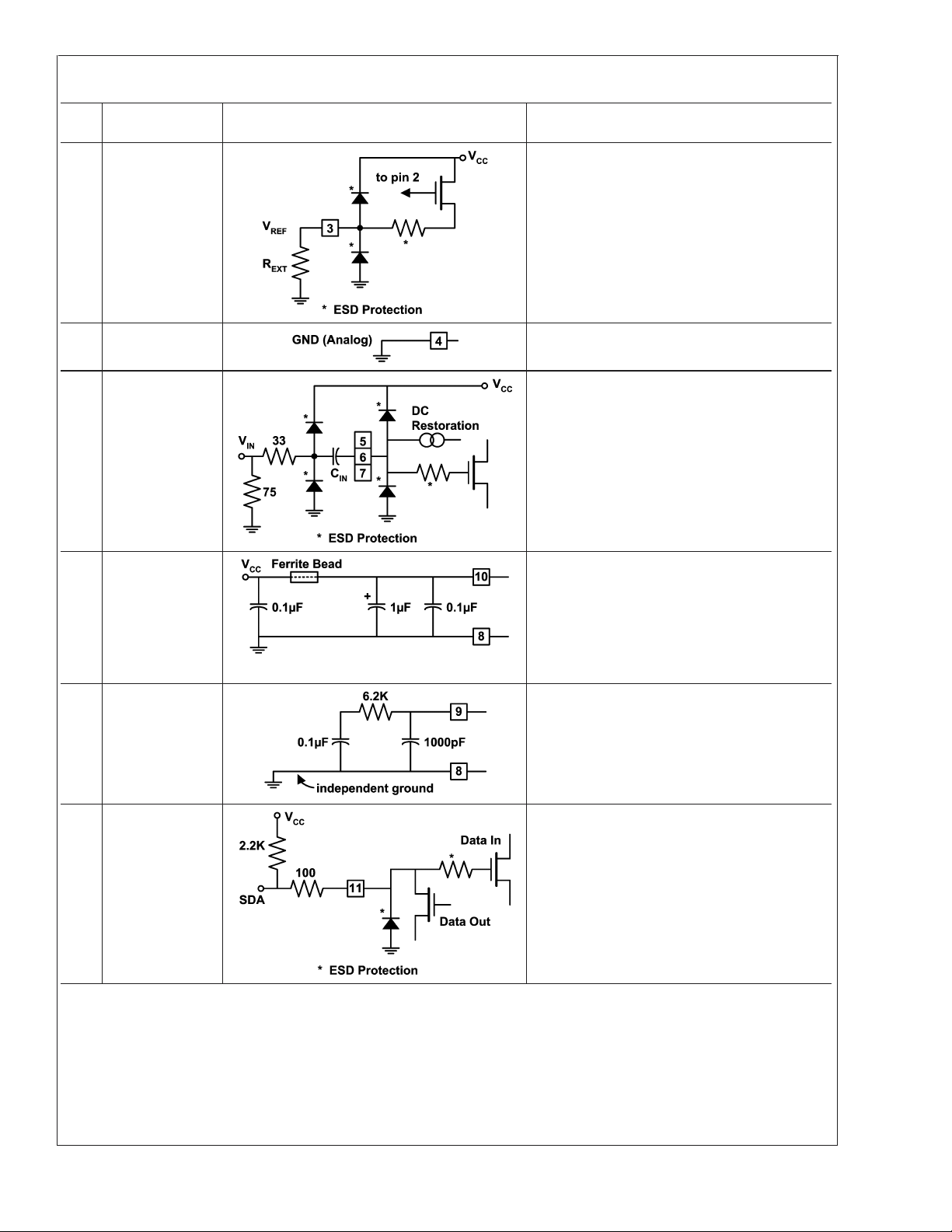
Pin Descriptions and Application Information (Continued)
LM1246
Pin
No.
3V
Pin Name Schematic Description
REF
4 Analog Input
Ground
5
Blue Video In
6
7
8
10
Red Video In
Green Video In
Digital Ground
PLL V
CC
9 PLL Filter
External resistor, 10k 1%, sets the internal bias
current level for optimum performance of the
LM1247. This resistor should be placed as close
to pin 3 and the pin 4 ground return as possible.
This is the ground for the input analog portions
of the LM1247 internal circuitry.
These video inputs must be AC coupled with a
.0047 µF cap. Internal DC restoration is done at
these inputs. A series resistor of about 33Ω and
external ESD protection diodes should also be
used for protection from ESD damage.
The ground pin should be connected to the rest
of the circuit ground by a short but independent
PCB trace to prevent contamination by
extraneous signals. The V
isolated from the rest of the V
pin should be
CC
line by a ferrite
CC
bead and bypassed to pin 8 with an electrolytic
capacitor and a high frequency ceramic.
Recommended topology and values are shown
to the left. It is recommended that both filter
branches be bypassed to the independent
ground as close to pin 8 as possible. Great care
should be taken to prevent external signals from
2
coupling into this filter from video, I
C, etc.
11 SDA
The I2C compatible data line. A pull-up resistor
of about 2 kΩ should be connected between this
pin and V
. A resistor of at least 100Ω should
CC
be connected in series with the data line for
additional ESD protection.
www.national.com11

Pin Descriptions and Application Information (Continued)
LM1246
Pin
No.
12 SCL The I2C compatible clock line. A pull-up resistor
Pin Name Schematic Description
of about 2 kΩ should be connected between this
pin and V
. A resistor of at least 100Ω should
CC
be connected in series with the clock line for
additional ESD protection.
13
14
15
16
17
18
19
20
21
DAC 4 Output
DAC 2 Output
DAC 3 Output
DAC 1 Output
Ground
V
CC
Green Output
Red Output
Blue Output
DAC outputs for cathode cut-off adjustments and
brightness control. DAC 4 can be set to change
the outputs of the other three DACs, acting as a
brightness control. The DAC values and the
2
special DAC 4 function are set through the I
C
compatible bus. A resistor of at least 100Ω
should be connected in series with these outputs
for additional ESD protection.
Ground pin for the output analog portion of the
LM1247 circuitry, and power supply pin for all
the analog of the LM1247. Note the
recommended charge storage and high
frequency capacitors which should be as close to
pins 17 and 18 as possible.
These are the three video output pins. They are
intended to drive the LM246x family of cathode
drivers. Nominally, about 2V peak to peak will
produce 40V peak to peak of cathode drive.
22 ABL
www.national.com 12
The Automatic Beam Limiter input is biased to
the desired beam current limit by R
and normally keeps D
forward biased. When
INT
ABL
and V
the current resupplying the CRT capacitance
(averaged by C
) exceeds this limit, then D
ABL
begins to turn off and the voltage at pin 22
begins to drop. The LM1247 then lowers the
gain of the three video channels until the beam
current reaches an equilibrium value.
BB
INT
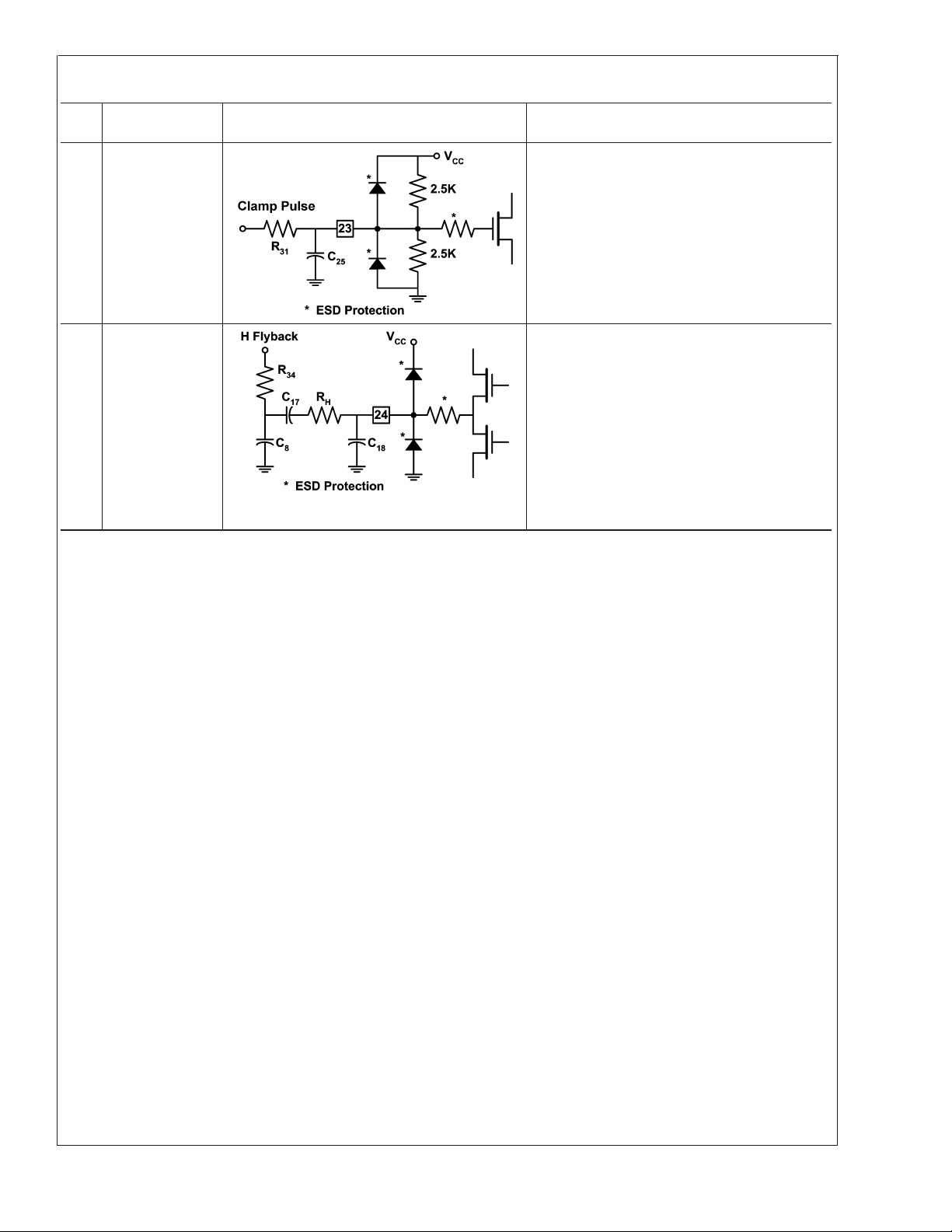
Pin Descriptions and Application Information (Continued)
LM1246
Pin
No.
Pin Name Schematic Description
23 CLAMP This pin accepts either TTL or CMOS logic
levels. The internal switching threshold is
approximately one-half of V
series resistor, R
, of about 1K is recommended
31
. An external
CC
to avoid overdriving the input devices. In any
event, R
must be large enough to prevent the
EXT
voltage at pin 23 from going higher than V
below GND.
24 H Flyback
Proper operation requires current reversal. R
should be large enough to limit the peak current
at pin 24 to about +4 ma during blanking, and
−500 µA during scan. C
is usually needed for
17
logic level inputs and should be large enough to
make the time constant, R
larger than the horizontal period. R
HC17
significantly
and C8are
34
typically 300Ω and 330 pF when the flyback
waveform has ringing and needs filtering. C
may be needed to filter extraneous noise and
can be up to 100 pF.
or
CC
H
18
www.national.com13
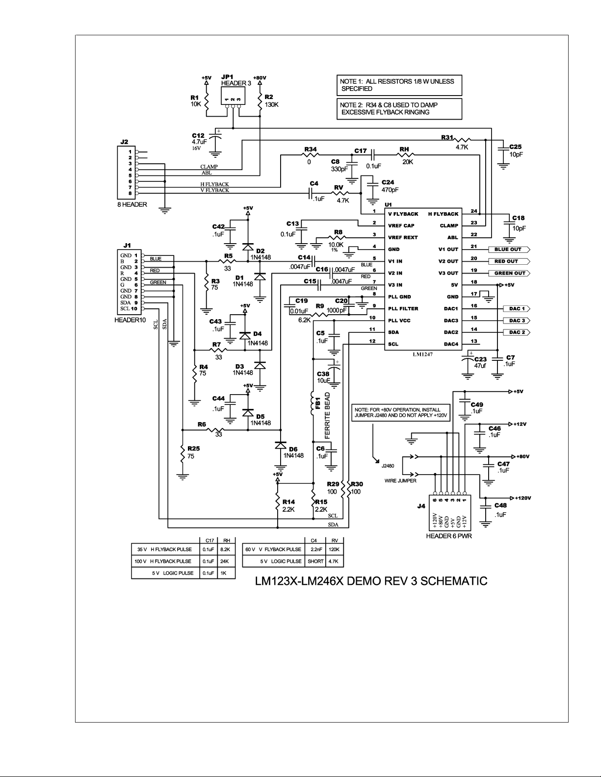
Schematic Diagram
LM1246
FIGURE 9. LM123x/LM124x-LM246x Demo Board Schematic
www.national.com 14
20068524
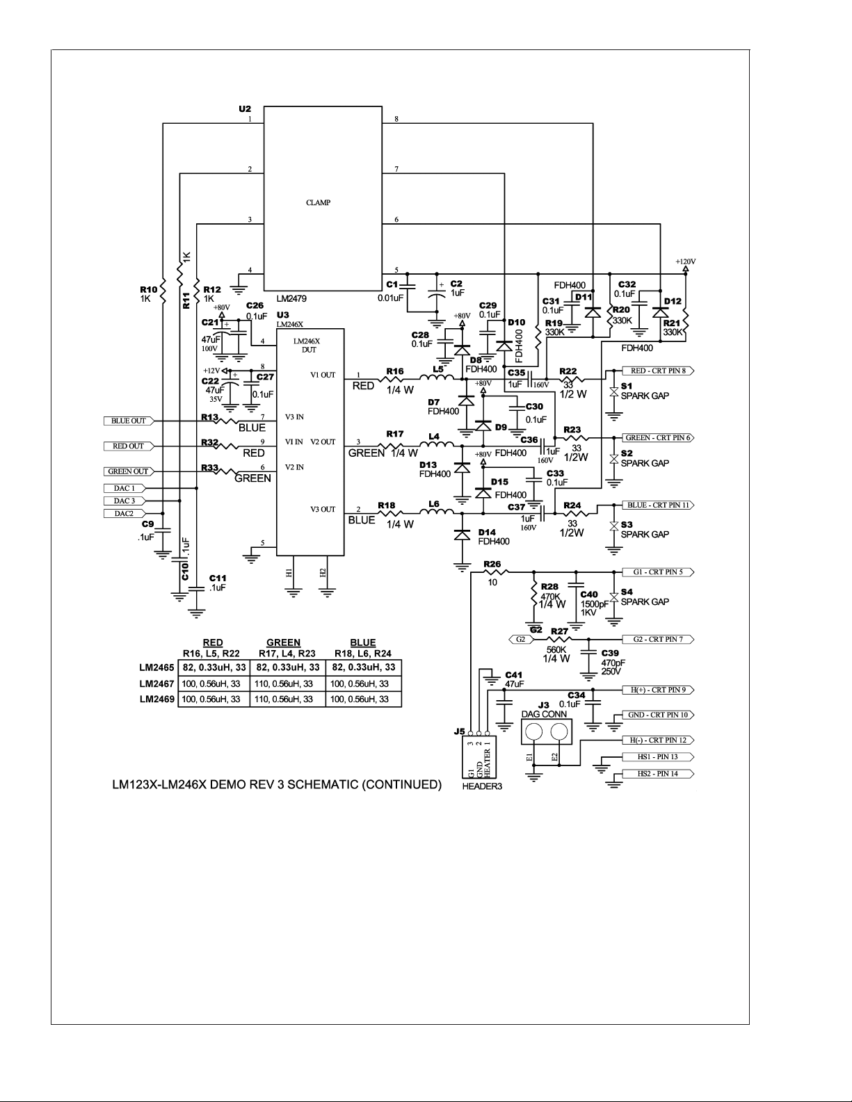
Schematic Diagram
LM1246
FIGURE 10. LM123x/LM124x-LM246x Demo Board Schematic (continued)
20068525
www.national.com15
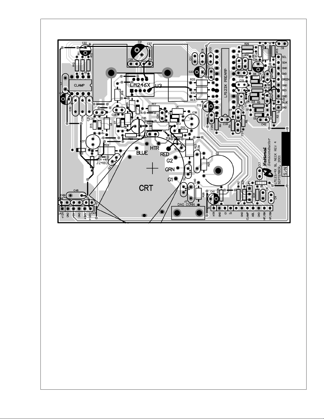
PCB Layout
LM1246
FIGURE 11. LM123x/LM124x-LM246x Demo Board Layout
20068526
www.national.com 16
 Loading...