

National Semiconductor LM117HV, LM317HV Technical data
查询LM117HV供应商
LM117HV/LM317HV
3-Terminal Adjustable Regulator
LM117HV/LM317HV 3-Terminal Adjustable Regulator
April 2000
General Description
The LM117HV/LM317HV are adjustable 3-terminal positive
voltage regulators capable of supplying in excess of 1.5A
over a 1.2V to 57V output range. They are exceptionally
easy to use and require only two external resistors to set the
output voltage. Further, both line andloadregulation are better than standard fixed regulators. Also, the LM117HV is
packaged in standard transistor packages which are easily
mounted and handled.
In addition to higher performance than fixed regulators, the
LM117HVseries offers full overload protection available only
in IC’s. Included on the chip are current limit, thermal overload protection and safe area protection. All overload protection circuitry remains fully functional even if the adjustment
terminal is disconnected.
Normally,no capacitors are needed unless the device is situated more than 6 inches from the input filter capacitors in
which case an input bypass is needed. An optional output
capacitor can be added to improve transient response. The
adjustment terminal can be bypassed to achieve very high
ripple rejections ratios which are difficult to achieve with
standard 3-terminal regulators.
Besides replacing fixed regulators, the LM117HV is useful in
a wide variety of other applications. Since the regulator is
“floating” and sees only the input-to-output differential voltage, supplies of several hundred volts can be regulated as
long as the maximum input to output differential is not exceeded, i.e. do not short the output to ground.
Also, it makes an especially simple adjustable switching
regulator,a programmable output regulator,or by connecting
a fixed resistor between the adjustment and output, the
LM117HVcan be used as a precision current regulator.Supplies with electronic shutdown can be achieved by clamping
the adjustment terminal to ground which programs the output to 1.2V where most loads draw little current.
The LM117HVK STEEL and LM317HVK STEEL are packaged in standard TO-3 transistor packages, while the
LM117HVH and LM317HVH are packaged in a solid Kovar
base TO-39 transistor package. The LM317HVT uses a TO220 plastic package. The LM117HV is rated for operation
from −55˚C to +150˚C, and the LM317HV from 0˚C to
+125˚C.
Features
n Adjustable output down to 1.2V
n Guaranteed 1.5A output current
n Line regulation typically 0.01%/V
n Load regulation typically 0.1%
n Current limit constant with temperature
n 100% electrical burn-in
n Eliminates the need to stock many voltages
n Standard 3-lead transistor package
n 80 dB ripple rejection
n Output is short-circuit protected
+
n P
Product Enhancement tested
Typical Applications
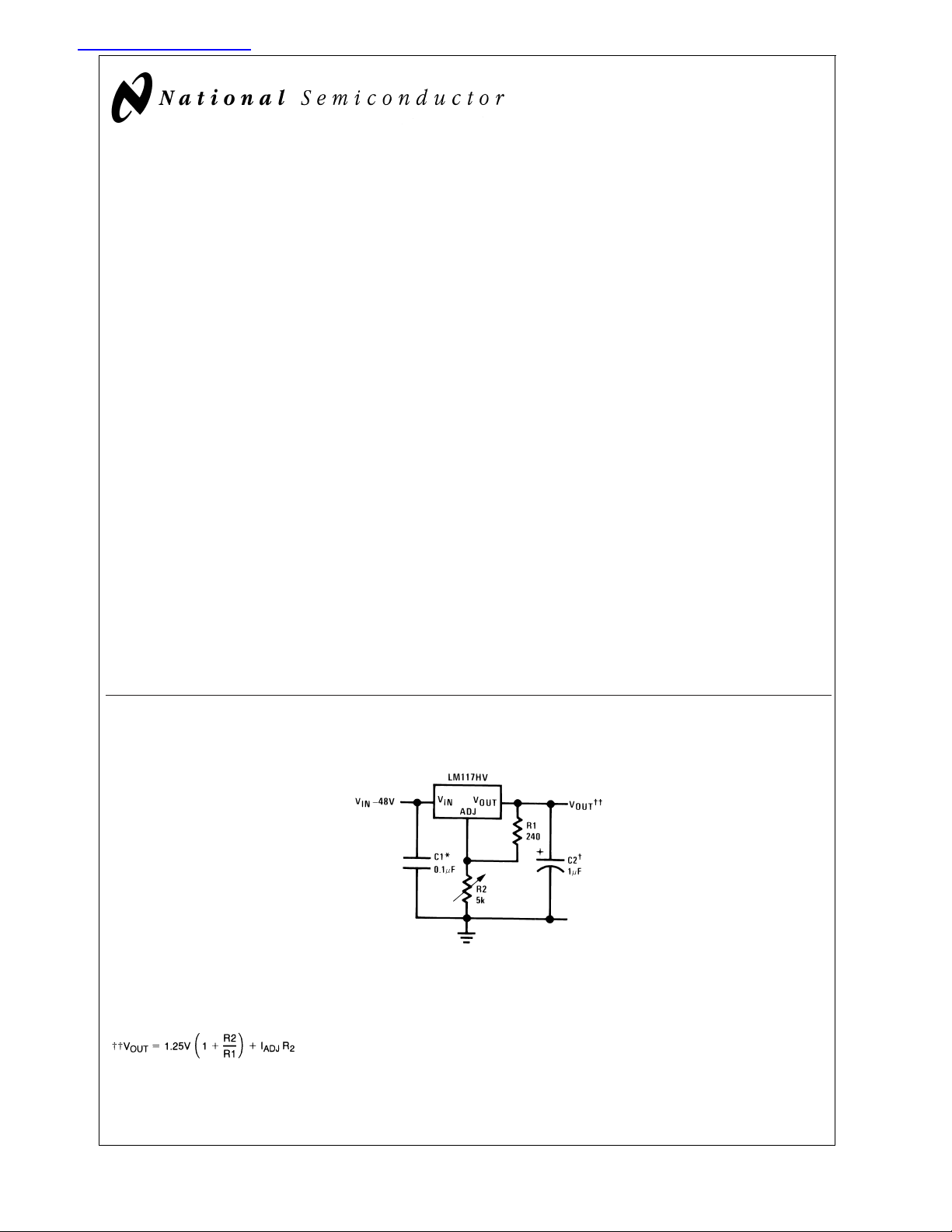
1.2V-45V Adjustable Regulator
DS009062-1
Full output current not available at high input-output voltages
†
Optional—improves transient response. Output capacitors in the range of 1 µF to 1000 µF of aluminum or tantalum electrolytic
are commonly used to provide improved output impedance and rejection of transients.
*Needed if device is more than 6 inches from filter capacitors.
© 2000 National Semiconductor Corporation DS009062 www.national.com
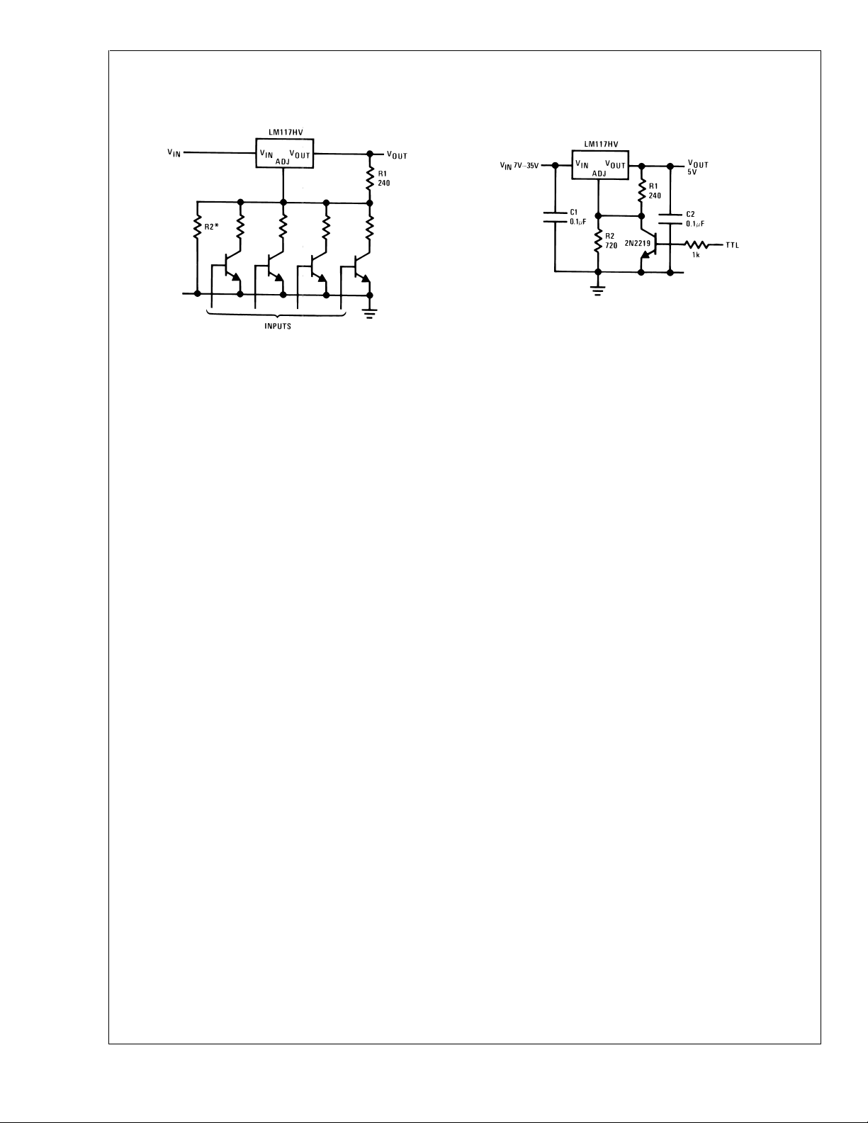
Typical Applications (Continued)
LM117HV/LM317HV
*Sets maximum V
Digitally Selected Outputs
OUT
DS009062-2
*Min. output ≈ 1.2V
5V Logic Regulator with
Electronic Shutdown
*
DS009062-3
www.national.com 2
LM117HV/LM317HV
Absolute Maximum Ratings (Note 1)
If Military/Aerospace specified devices are required,
please contact the National Semiconductor Sales Office/
Distributors for availability and specifications.
(Note 4)
Power Dissipation Internally limited
Operating Junction Temperature Range
LM117HV −55˚C to +150˚C
LM317HV 0˚C to +125˚C
Storage Temperature −65˚C to +150˚C
Lead Temperature (Soldering, 10 sec.) 300˚C
ESD Tolerance (Note 5) 2000V
Input—Output Voltage Differential +60V, −0.3V
Electrical Characteristics (Note 2)
Parameter Conditions LM117HV LM317HV Units
Min Typ Max Min Typ Max
Line Regulation T
Load Regulation T
Thermal Regulation T
Adjustment Pin Current 50 100 50 100 µA
Adjustment Pin Current Change 10 mA ≤ I
Reference Voltage 3.0 V ≤ (V
Line Regulation 3.0V ≤ (VIN−V
Load Regulation 10 mA ≤ I
Temperature Stability T
Minimum Load Current (V
Current Limit (V
RMS Output Noise, % of V
OUT
Ripple Rejection Ratio V
Long-Term Stability T
Thermal Resistance, H Package 12 15 12 15 ˚C/W
Junction to Case T Package 4 5 ˚C/W
Thermal Resistance, H Package 140 140 ˚C/W
Junction to Ambient T Package 50 ˚C/W
(no heat sink) K Package 35 35 ˚C/W
Note 1: “Absolute Maximum Ratings” indicate limits beyond which damage to the device may occur. Operating Ratings indicate conditions for which the device is
functional, but do not guarantee specific performance limits.
Note 2: Unless otherwise specified, these specifications apply: −55˚C ≤ T
= 0.1A for the TO-39 package and I
and I
OUT
applicable for power dissipations of 2W for the TO-39 and 20W for the TO-3 and TO-220. I
Note 3: Regulation is measured at constant junction temperature. Changes in output voltage due to heating effects must be taken into account separately.Pulse test-
ing with low duty cycle is used.
Note 4: Refer to RETS117HVH for LM117HVH or RETS117HVK for LM117HVK military specificatioins.
Note 5: Human body model, 1.5 kΩ in series with 100 pF.
= 25˚C, 3V ≤ VIN−V
J
(Note 3) I
= 25˚C, 10 mA ≤ I
J
= 25˚C, 20 ms Pulse 0.03 0.07 0.04 0.07 %/W
J
3.0 V ≤ (V
10 mA ≤ I
I
= 10 mA, (Note 3)
L
MIN
IN−VOUT
IN−VOUT
=10mA
L
≤ I
L
MAX
IN−VOUT
IN−VOUT
OUT
OUT
≤ TJ≤ T
) ≤ 60V
) ≤ 60V, (Note 4) 1.20 1.25 1.30 1.20 1.25 1.30 V
≤ I
MAX
) ≤ 60V, 0.02 0.05 0.02 0.07 %/V
OUT
≤ I
MAX
MAX
) = 60V 3.5 7 3.5 12 mA
) ≤ 15V
≤ 60V 0.01 0.02 0.01 0.04 %/V
OUT
OUT
≤ I
MAX
0.1 0.3 0.1 0.5 %
0.2 5 0.2 5 µA
,P≤P
MAX
(Note 3) 0.3 1 0.3 1.5 %
11%
K, T Packages 1.5 2.2 3.5 1.5 2.2 3.7 A
H Package 0.5 0.8 1.8 0.5 0.8 1.9 A
(V
IN−VOUT
) ≤ 60V
K, T Packages 0.3 0.3 A
H Package 0.03 0.03 A
TJ= 25˚C, 10 Hz ≤ f ≤ 10 kHz 0.003 0.003 %
= 10V, f = 120 Hz 65 65 dB
OUT
C
=10µF 6680 6680 dB
ADJ
= 125˚C 0.3 1 0.3 1 %
J
K Package 2.3 3 2.3 3 ˚C/W
≤ +150˚C for the LM117HV, and 0˚C ≤ TJ≤ +125˚C for the LM317HV; VIN−V
= 0.5A for the TO-3 and TO-220 packages. Although power dissipation is internally limited, these specifications are
OUT
J
is 1.5A for the TO-3 and TO-220 and 0.5A for the TO-39 package.
MAX
OUT
=5V
www.national.com3
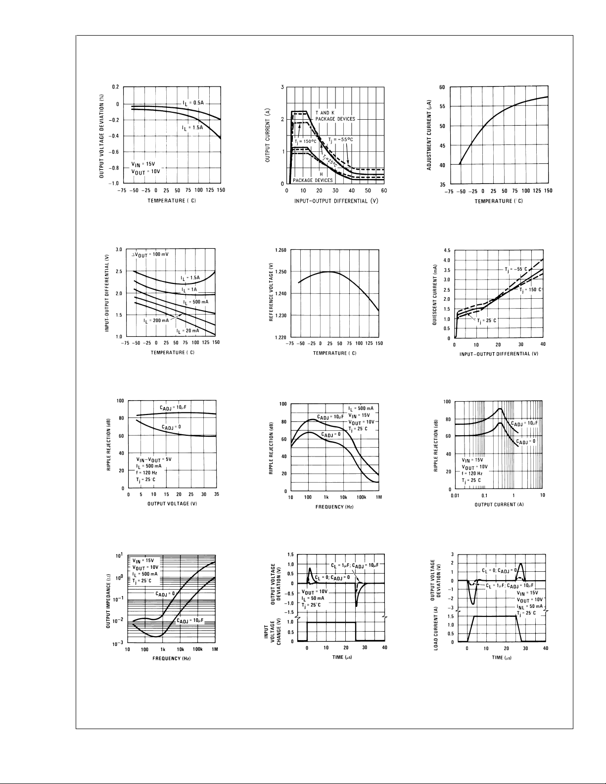
Typical Performance Characteristics Output capacitor = 0 µF unless otherwise noted.
Load Regulation
LM117HV/LM317HV
Dropout Voltage
DS009062-32
DS009062-35
Current Limit
Temperature Stability
DS009062-33
DS009062-36
Adjustment Current
DS009062-34
Minimum Operating Current
DS009062-37
Ripple Rejection
Output Impedance
DS009062-38
DS009062-41
Ripple Rejection
Line Transient Response
DS009062-39
DS009062-42
Ripple Rejection
DS009062-40
Load Transient Response
DS009062-43
www.national.com 4
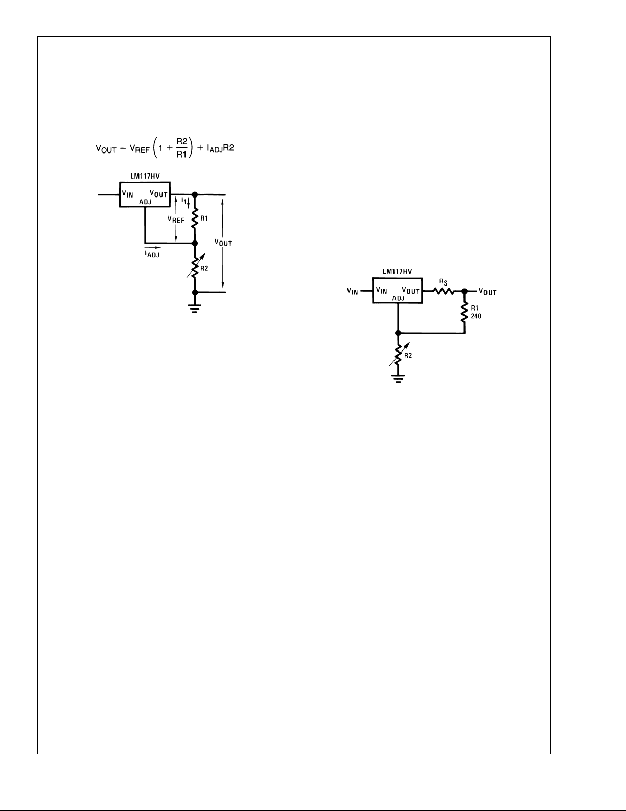
Application Hints
In operation, the LM117HV develops a nominal 1.25V reference voltage, V
minal. The reference voltage is impressed across program
resistor R1 and, since the voltage is constant, a constant
current I
then flows through the output set resistor R2, giv-
1
ing an output voltage of
, between the output and adjustment ter-
REF
DS009062-5
FIGURE 1.
insures stability. Any increase of load capacitance larger
than 10 µF will merely improve the loop stability and output
impedance.
Load Regulation
The LM117HV is capable of providing extremely good load
regulation but a few precautions are needed to obtain maximum performance. The current set resistor connected between the adjustment terminal and the output terminal (usually 240Ω) should be tied directly to the output of the
regulator rather than near the load. This eliminates line
drops from appearing effectively in series with the reference
and degrading regulation. For example, a 15V regulator with
0.05Ω resistance between the regulator and load will have a
load regulation due to line resistance of 0.05Ω xI
. If the set
L
resistor is connected near the load the effective line resistance will be 0.05Ω (1 + R2/R1) or in this case, 11.5 times
worse.
Figure 2
shows the effect of resistance between the regula-
tor and 240Ω set resistor.
LM117HV/LM317HV
Since the 100 µA current from the adjustment terminal represents an error term, the LM117HVwas designed to minimize
I
and make it very constant with line and load changes.
ADJ
To do this, all quiescent operating current is returned to the
output establishing a minimum load current requirement. If
there is insufficient load on the output, the output will rise.
External Capacitors
An input bypass capacitor is recommended. A 0.1 µF disc or
1 µF solid tantalum on the input is suitable input bypassing
for almost all applications. The device is more sensitive to
the absence of input bypassing when adjustment or output
capacitors are used but the above values will eliminate the
possiblity of problems.
The adjustment terminal can be bypassed to ground on the
LM117HV to improve ripple rejection. This bypass capacitor
prevents ripple from being amplified as the output voltage is
increased. With a 10 µF bypass capacitor 80 dB ripple rejection is obtainable at any output level. Increases over 10 µF
do not appreciably improve the ripple rejection at frequencies above 120 Hz. If the bypass capacitor is used, it is
sometimes necessary to include protection diodes to prevent
the capacitor from discharging through internal low current
paths and damaging the device.
In general, the best type of capacitors to use are solid tantalum. Solid tantalum capacitors have low impedance even at
high frequencies. Depending upon capacitor construction, it
takes about 25 µF in aluminum electrolytic to equal 1 µF
solid tantalum at high frequencies. Ceramic capacitors are
also good at high frequencies; but some types have a large
decrease in capacitance at frequencies around 0.5 MHz. For
this reason, 0.01 µF disc may seem to work better than a 0.1
µF disc as a bypass.
Although the LM117HV is stable with no output capacitors,
like any feedback circuit, certain values of external capacitance can cause excessive ringing. This occurs with values
between 500 pF and 5000 pF.A1 µF solid tantalum (or 25 µF
aluminum electrolytic) on the output swamps this effect and
DS009062-6
FIGURE 2. Regulator with Line
Resistance in Output Lead
With the TO-3 package, it is easy to minimize the resistance
from the case to the set resistor, by using two separate leads
to the case. However, with the TO-5 package, care should be
taken to minimize the wire length of the output lead. The
ground of R2 can be returned near the ground of the load to
provide remote ground sensing and improve load regulation.
Protection Diodes
When external capacitors are used with
any
IC regulator it is
sometimes necessary to add protection diodes to prevent
the capacitors from discharging through low current points
into the regulator. Most 10 µF capacitors have low enough
internal series resistance to deliver 20A spikes when
shorted. Although the surge is short, there is enough energy
to damage parts of the IC.
When an output capacitor is connected to a regulator and
the input is shorted, the output capacitor will discharge into
the output of the regulator. The discharge current depends
on the value of the capacitor, the output voltage of the regulator, and the rate of decrease of V
. In the LM117HV, this
IN
discharge path is through a large junction that is able to sustain 15A surge with no problem. This is not true of other
types of positive regulators. For output capacitors of 25 µF or
less, there is no need to use diodes.
The bypass capacitor on the adjustment terminal can discharge through a low current junction. Discharge occurs
when
either
the input or output is shorted. Internal to the
LM117HV is a 50Ω resistor which limits the peak discharge
current. No protection is needed for output voltages of 25V
www.national.com5
 Loading...