

National Semiconductor LM111, LM211, LM311 Technical data
查询LM111供应商
LM111/LM211/LM311
Voltage Comparator
1.0 General Description
The LM111, LM211 and LM311 are voltage comparators that
have input currents nearly a thousand times lower than
devices like the LM106 or LM710. They are also designed to
operate over a wider range of supply voltages: from standard
±
15V op amp supplies down to the single 5V supply used for
IC logic. Their output is compatible with RTL, DTL and TTL
as well as MOS circuits. Further, they can drive lamps or
relays, switching voltages up to 50V at currents as high as
50 mA.
Both the inputs and the outputs of the LM111, LM211 or the
LM311 can be isolated from system ground, and the output
can drive loads referred to ground, the positive supply or the
negative supply. Offset balancing and strobe capability are
provided and outputs can be wire OR’ed. Although slower
than the LM106 and LM710 (200 ns response time vs 40 ns)
January 2001
the devices are also much less prone to spurious oscillations. The LM111 has the same pin configuration as the
LM106 and LM710.
The LM211 is identical to the LM111, except that its performance is specified over a −25˚C to +85˚C temperature range
instead of −55˚C to +125˚C. The LM311 has a temperature
range of 0˚C to +70˚C.
2.0 Features
n Operates from single 5V supply
n Input current: 150 nA max. over temperature
n Offset current: 20 nA max. over temperature
n Differential input voltage range:
n Power consumption: 135 mW at
±
30V
±
15V
LM111/LM211/LM311 Voltage Comparator
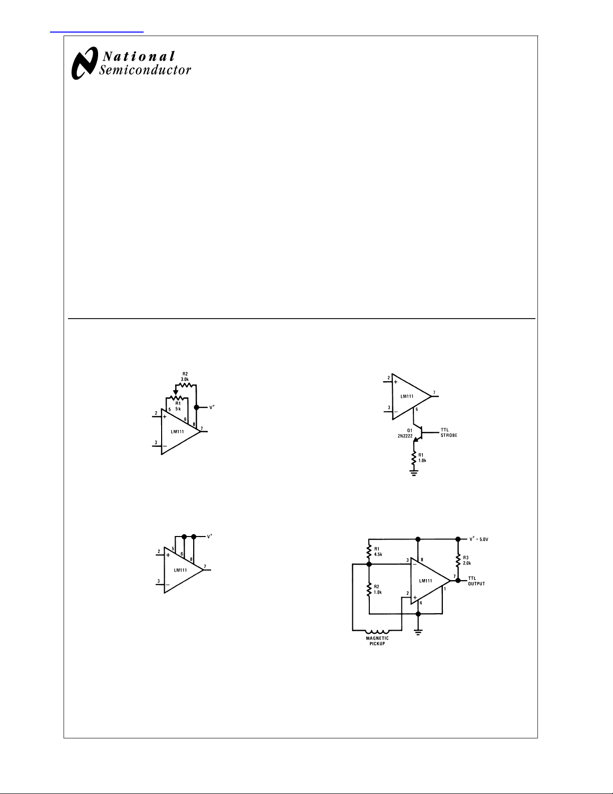
3.0 Typical Applications (Note 3)
Offset Balancing Strobing
00570436
Increasing Input Stage Current (Note 1) Detector for Magnetic Transducer
00570438
Note 1: Increases typical common mode slew from 7.0V/µs to 18V/µs.
Note: Do Not Ground Strobe Pin. Output is turned off when current is
00570437
pulled from Strobe Pin.
00570439
© 2004 National Semiconductor Corporation DS005704 www.national.com
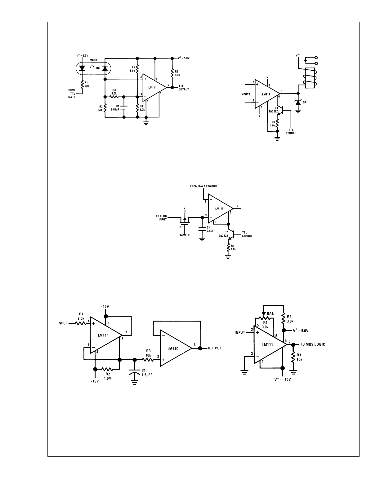
3.0 Typical Applications (Note 3) (Continued)
Digital Transmission Isolator Relay Driver with Strobe
LM111/LM211/LM311
00570440
*Absorbs inductive kickback of relay and protects IC from severe voltage
transients on V
Note: Do Not Ground Strobe Pin.
++
line.
Strobing off Both Input and Output Stages (Note 2)
Note: Do Not Ground Strobe Pin.
Note 2: Typical input current is 50 pA with inputs strobed off.
Note 3: Pin connections shown on schematic diagram and typical applications are for H08 metal can package.
00570442
Positive Peak Detector Zero Crossing Detector Driving MOS Logic
00570441
*Solid tantalum
00570423
www.national.com 2
00570424
LM111/LM211/LM311
4.0 Absolute Maximum Ratings for
the LM111/LM211
If Military/Aerospace specified devices are required,
please contact the National Semiconductor Sales Office/
Distributors for availability and specifications.
Total Supply Voltage (V
Output to Negative Supply Voltage
) 50V
(V
74
Ground to Negative Supply Voltage
) 30V
(V
14
Differential Input Voltage
Input Voltage (Note 4)
Output Short Circuit Duration 10 sec
Operating Temperature Range
(Note 10)
) 36V
84
±
±
30V
15V
LM111 −55˚C to 125˚C
LM211 −25˚C to 85˚C
Lead Temperature (Soldering, 10 sec) 260˚C
Voltage at Strobe Pin V
+
Soldering Information
Dual-In-Line Package
Soldering (10 seconds) 260˚C
Small Outline Package
Vapor Phase (60 seconds) 215˚C
Infrared (15 seconds) 220˚C
See AN-450 “Surface Mounting Methods and Their Effect
on Product Reliability” for other methods of soldering
surface mount devices.
ESD Rating (Note 11) 300V
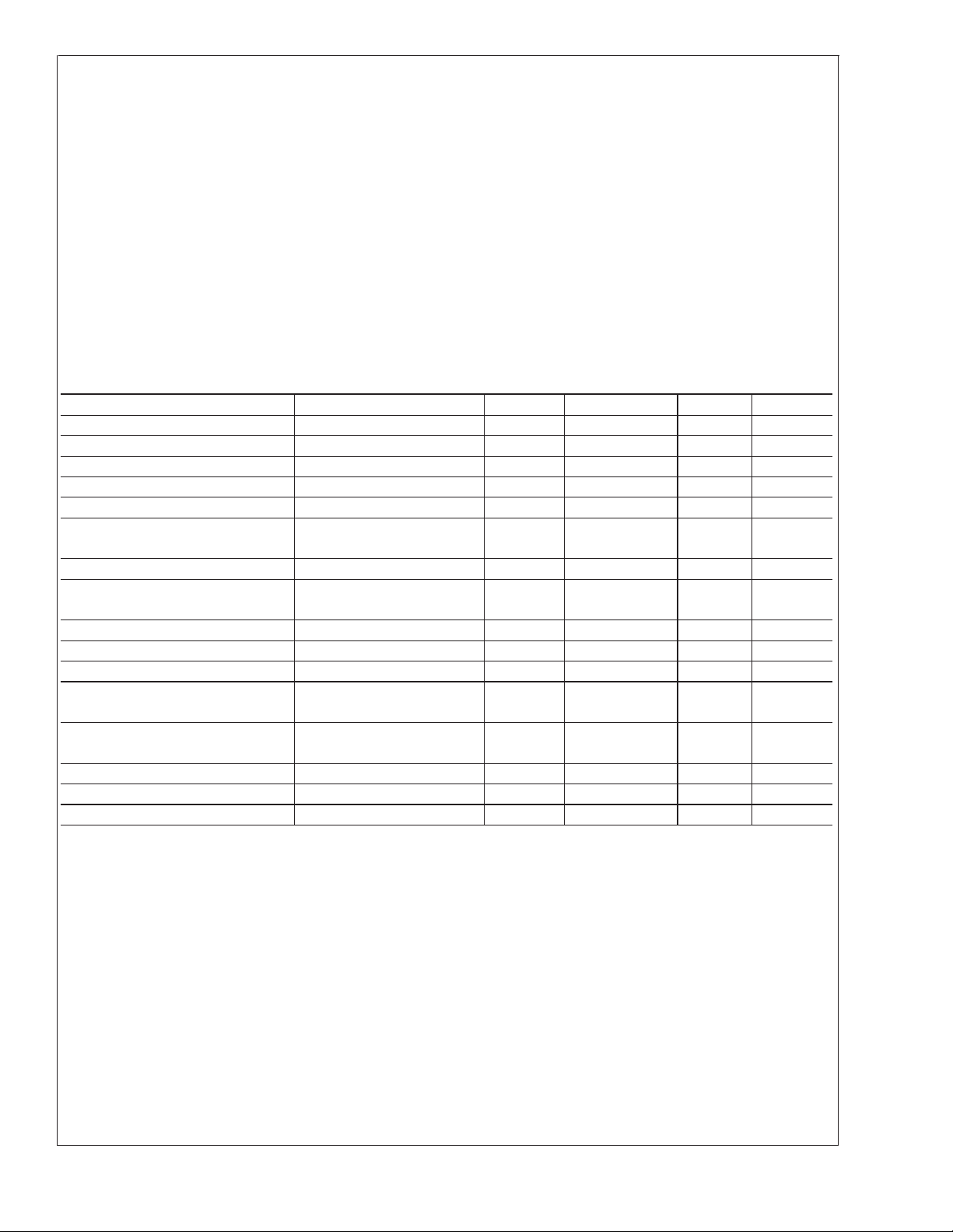
Electrical Characteristics (Note 6) for the LM111 and LM211
Parameter Conditions Min Typ Max Units
Input Offset Voltage (Note 7) T
Input Offset Current T
Input Bias Current T
Voltage Gain T
Response Time (Note 8) T
Saturation Voltage V
Strobe ON Current (Note 9) T
Output Leakage Current V
Input Offset Voltage (Note 7) R
Input Offset Current (Note 7) 20 nA
Input Bias Current 150 nA
Input Voltage Range V
Saturation Voltage V
Output Leakage Current V
Positive Supply Current T
Negative Supply Current T
Note 4: This rating applies for±15 supplies. The positive input voltage limit is 30V above the negative supply. The negative input voltage limit is equal to the
negative supply voltage or 30V below the positive supply, whichever is less.
Note 5: The maximum junction temperature of the LM111 is 150˚C, while that of the LM211 is 110˚C. For operating at elevated temperatures, devices in the H08
package must be derated based on a thermal resistance of 165˚C/W, junction to ambient, or 20˚C/W, junction to case. The thermal resistance of the dual-in-line
package is 110˚C/W, junction to ambient.
Note 6: These specifications apply for V
temperature specifications are limited to −25˚C≤T
5V supply up to
Note 7: The offset voltages and offset currents given are the maximum values required to drive the output within a volt of either supply witha1mAload. Thus, these
parameters define an error band and take into account the worst-case effects of voltage gain and R
Note 8: The response time specified (see definitions) is for a 100 mV input step with 5 mV overdrive.
Note 9: This specification gives the range of current which must be drawn from the strobe pin to ensure the output is properly disabled. Do not short the strobe pin
to ground; it should be current driven at 3 to 5 mA.
Note 10: Refer to RETS111X for the LM111H, LM111J and LM111J-8 military specifications.
Note 11: Human body model, 1.5 kΩ in series with 100 pF.
±
15V supplies.
=25˚C, RS≤50k 0.7 3.0 mV
A
=25˚C 4.0 10 nA
A
=25˚C 60 100 nA
A
=25˚C 40 200 V/mV
A
=25˚C 200 ns
A
≤−5 mV, I
IN
T
=25˚C
A
=25˚C 2.0 5.0 mA
A
≥5 mV, V
IN
T
=25˚C, I
A
≤50 k 4.0 mV
S
+
=15V, V−=−15V, Pin 7 −14.5 13.8,-14.7 13.0 V
=50 mA 0.75 1.5 V
OUT
=35V 0.2 10 nA
OUT
=3 mA
STROBE
Pull-Up May Go To 5V
+
≥4.5V, V−=0 0.23 0.4 V
V
≤−6 mV, I
IN
≥5 mV, V
IN
=25˚C 5.1 6.0 mA
A
=25˚C 4.1 5.0 mA
A
=±15V and Ground pin at ground, and −55˚C≤TA≤+125˚C, unless otherwise stated. With the LM211, however, all
S
≤+85˚C. The offset voltage, offset current and bias current specifications apply for any supply voltage from a single
A
≤8mA
OUT
=35V 0.1 0.5 µA
OUT
.
S
−5V
www.national.com3
5.0 Absolute Maximum Ratings for
the LM311
If Military/Aerospace specified devices are required,
please contact the National Semiconductor Sales Office/
Distributors for availability and specifications.
Total Supply Voltage (V
LM111/LM211/LM311
Output to Negative Supply Voltage
) 40V
(V
74
Ground to Negative Supply Voltage
) 30V
(V
14
Differential Input Voltage
Input Voltage (Note 13)
Power Dissipation (Note 14) 500 mW
ESD Rating (Note 19) 300V
(Note 12)
84
) 36V
±
±
30V
15V
Output Short Circuit Duration 10 sec
Operating Temperature Range 0˚ to 70˚C
Storage Temperature Range −65˚C to 150˚C
Lead Temperature (soldering, 10 sec) 260˚C
Voltage at Strobe Pin V
Soldering Information
Dual-In-Line Package
Soldering (10 seconds) 260˚C
Small Outline Package
Vapor Phase (60 seconds) 215˚C
Infrared (15 seconds) 220˚C
See AN-450 “Surface Mounting Methods and Their Effect
on Product Reliability” for other methods of soldering
surface mount devices.
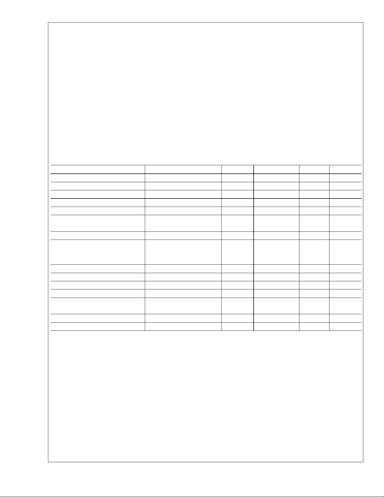
Electrical Characteristics (Note 15) for the LM311
Parameter Conditions Min Typ Max Units
Input Offset Voltage (Note 16) T
Input Offset Current(Note 16) T
Input Bias Current T
Voltage Gain T
Response Time (Note 17) T
Saturation Voltage V
Strobe ON Current (Note 18) T
Output Leakage Current V
Input Offset Voltage (Note 16) R
Input Offset Current (Note 16) 70 nA
Input Bias Current 300 nA
Input Voltage Range −14.5 13.8,−14.7 13.0 V
Saturation Voltage V
Positive Supply Current T
Negative Supply Current T
Note 12: “Absolute Maximum Ratings indicate limits beyond which damage to the device may occur. Operating Ratings indicate conditions for which the device is
functional, but do not guarantee specific performance limits.”
Note 13: This rating applies for
negative supply voltage or 30V below the positive supply, whichever is less.
Note 14: The maximum junction temperature of the LM311 is 110˚C. For operating at elevated temperature, devices in the H08 package must be derated based
on a thermal resistance of 165˚C/W, junction to ambient, or 20˚C/W, junction to case. The thermal resistance of the dual-in-line package is 100˚C/W, junction to
ambient.
Note 15: These specifications apply for V
bias current specifications apply for any supply voltage from a single 5V supply up to
Note 16: The offset voltages and offset currents given are the maximum values required to drive the output within a volt of either supply with 1 mA load. Thus, these
parameters define an error band and take into account the worst-case effects of voltage gain and R
Note 17: The response time specified (see definitions) is for a 100 mV input step with 5 mV overdrive.
Note 18: This specification gives the range of current which must be drawn from the strobe pin to ensure the output is properly disabled. Do not short the strobe
pin to ground; it should be current driven at 3 to 5 mA.
Note 19: Human body model, 1.5 kΩ in series with 100 pF.
±
15V supplies. The positive input voltage limit is 30V above the negative supply. The negative input voltage limit is equal to the
=25˚C, RS≤50k 2.0 7.5 mV
A
=25˚C 6.0 50 nA
A
=25˚C 100 250 nA
A
=25˚C 40 200 V/mV
A
=25˚C 200 ns
A
≤−10 mV, I
IN
T
=25˚C
A
=25˚C 2.0 5.0 mA
A
≥10 mV, V
IN
T
=25˚C, I
A
−
V
= Pin 1 = −5V
≤50K 10 mV
S
+
≥4.5V, V−=0 0.23 0.4 V
V
≤−10 mV, I
IN
=25˚C 5.1 7.5 mA
A
=25˚C 4.1 5.0 mA
A
=±15V and Pin 1 at ground, and 0˚C<T
S
=50 mA 0.75 1.5 V
OUT
=35V
OUT
=3 mA 0.2 50 nA
STROBE
≤8mA
OUT
<
+70˚C, unless otherwise specified. The offset voltage, offset current and
A
±
15V supplies.
.
S
+
−5V
www.national.com 4
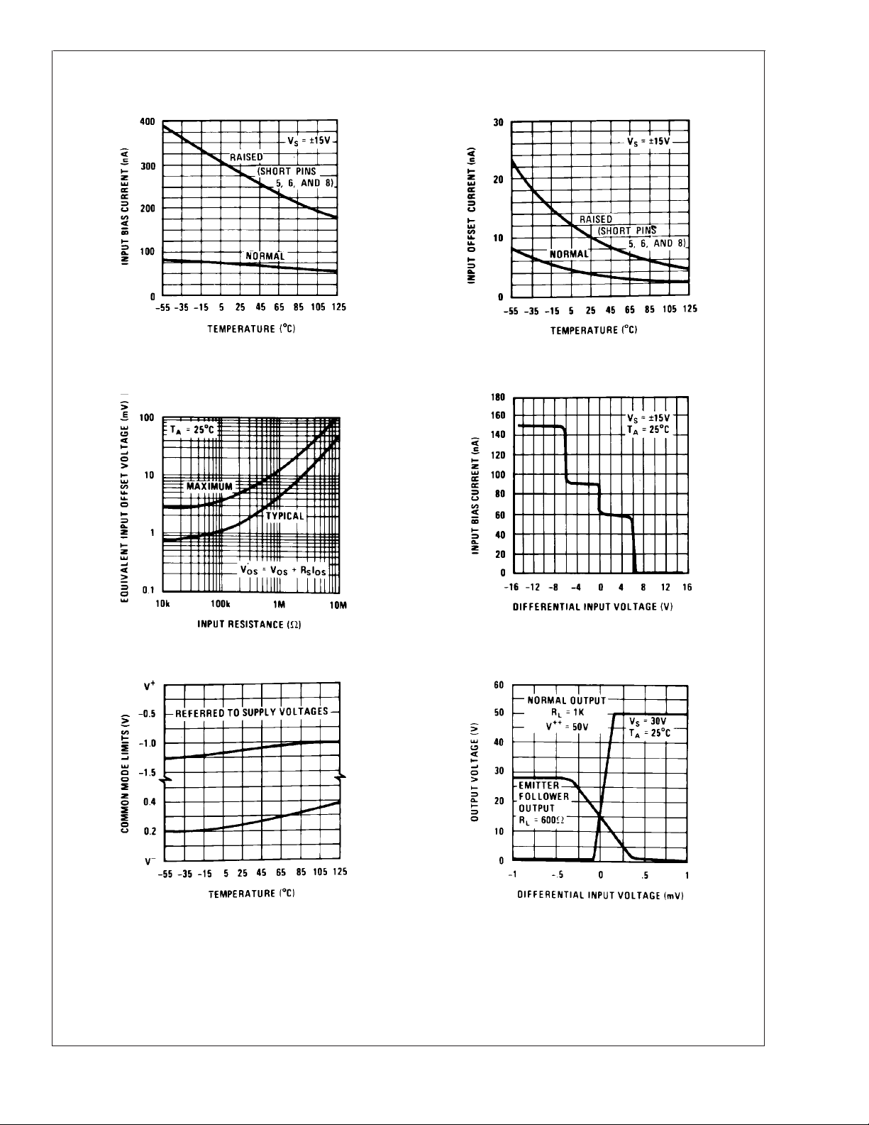
6.0 LM111/LM211 Typical Performance Characteristics
Input Bias Current Input Bias Current
LM111/LM211/LM311
00570443
Input Bias Current Input Bias Current
00570445
Input Bias Current Input Bias Current
00570444
00570446
00570447
00570448
www.national.com5
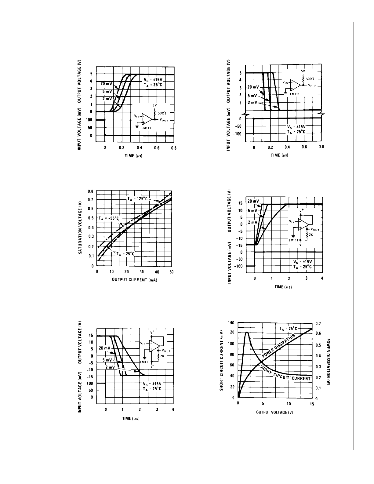
6.0 LM111/LM211 Typical Performance Characteristics (Continued)
Input Bias Current
Input Overdrives
Input Bias Current
Input Overdrives
LM111/LM211/LM311
00570450
Input Bias Current
00570449
Response Time for Various
Input Overdrives
00570451
Response Time for Various
Input Overdrives Output Limiting Characteristics
00570453
www.national.com 6
00570452
00570454
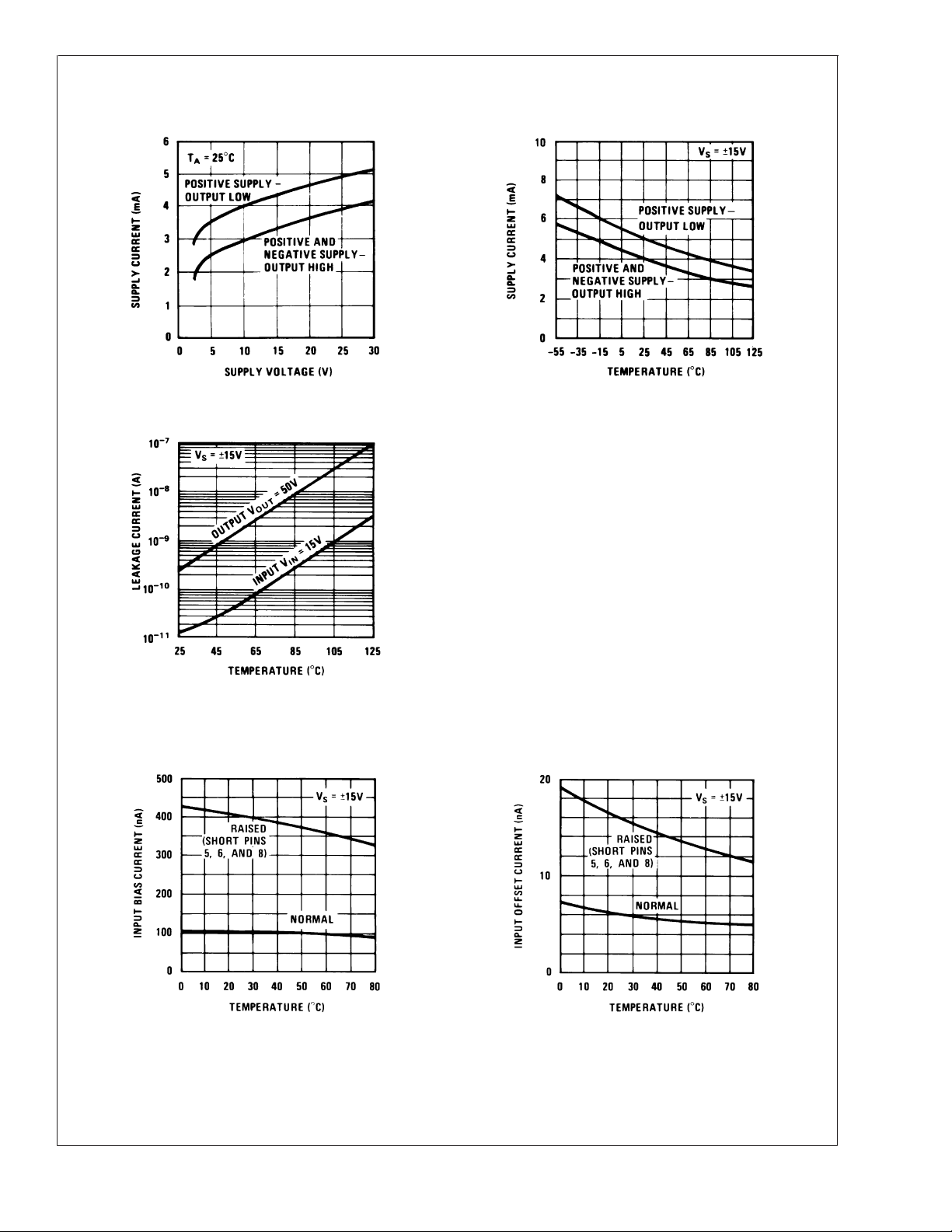
6.0 LM111/LM211 Typical Performance Characteristics (Continued)
Supply Current Supply Current
00570455 00570456
Leakage Currents
LM111/LM211/LM311
00570457
7.0 LM311 Typical Performance Characteristics
Input Bias Current Input Offset Current
00570458
00570459
www.national.com7
 Loading...