

National Semiconductor LM1084 Technical data
查询LM1084供应商
LM1084
5A Low Dropout Positive Regulators
LM1084 5A Low Dropout Positive Regulators
June 2005
General Description
The LM1084 is a series of low dropout voltage positive
regulators with a maximum dropout of 1.5V at 5A of load
current. It has the same pin-out as National Semiconductor’s
industry standard LM317.
The LM1084 is available in an adjustable version, which can
set the output voltage with only two external resistors. It is
also available in three fixed voltages: 3.3V, 5.0V and 12.0V.
The fixed versions intergrate the adjust resistors.
The LM1084 circuit includes a zener trimmed bandgap reference, current limiting and thermal shutdown.
The LM1084 series is available in TO-220 and TO-263 packages. Refer to the LM1085 for the 3A version, and the
LM1086 for the 1.5A version.
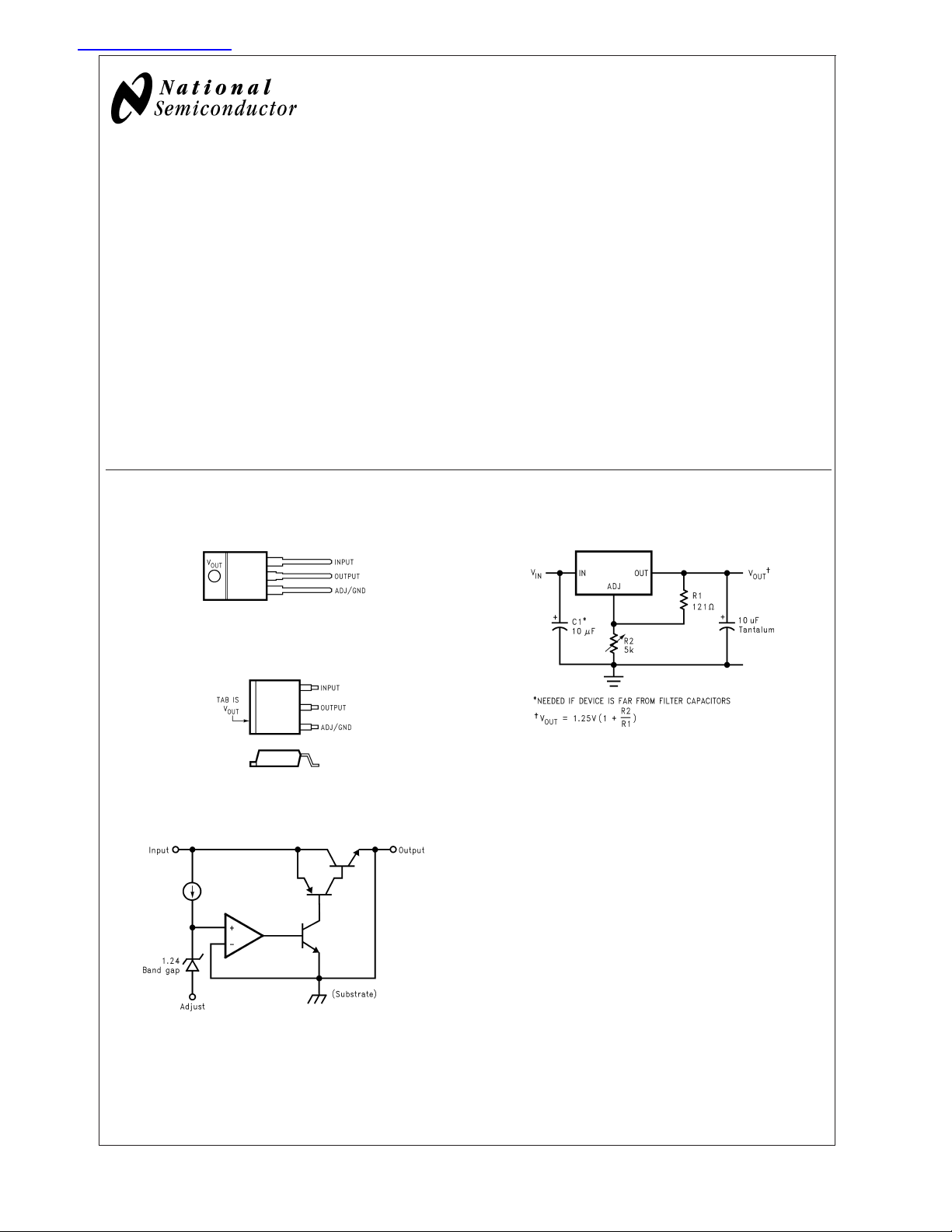
Connection Diagrams
TO-220
10094636
Top View
TO-263
Features
n Available in 3.3V, 5.0V, 12V and Adjustable Versions
n Current Limiting and Thermal Protection
n Output Current 5A
n Industrial Temperature Range −40˚C to 125˚C
n Line Regulation 0.015% (typical)
n Load Regulation 0.1% (typical)
Applications
n Post Regulator for Switching DC/DC Conveter
n High Efficiency Linear Regulators
n Battery Charger
Application Circuit
1.2V to 15V Adjustable Regulator
10094635
Top View
Basic Functional Diagram, Adjustable Version
10094665
© 2005 National Semiconductor Corporation DS100946 www.national.com
10094652
Ordering Information
LM1084
3-lead TO-263 −40˚C to +125˚C LM1084IS-ADJ Rails
3-lead TO-220 −40˚C to + 125˚C LM1084IT-ADJ Rails
Package Temperature Range Part Number Transport Media NSC Drawing
LM1084ISX-ADJ Tape and Reel
LM1084IS-12 Rails
LM1084ISX-12 Tape and Reel
LM1084IS-3.3 Rails
LM1084ISX-3.3 Tape and Reel
LM1084IS-5.0 Rails
LM1084ISX-5.0 Tape and Reel
LM1084IT-12 Rails
LM1084IT-3.3 Rails
LM1084IT-5.0 Rails
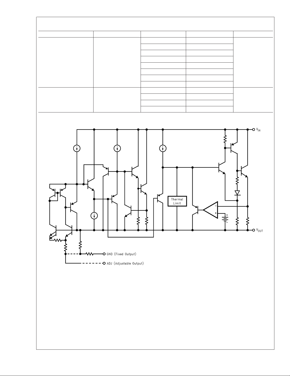
Simplified Schematic
TS3B
T03B
www.national.com 2
10094634
LM1084
Absolute Maximum Ratings (Note 1)
If Military/Aerospace specified devices are required,
please contact the National Semiconductor Sales Office/
Distributors for availability and specifications.
Junction Temperature (TJ)(Note 3) 150˚C
Storage Temperature Range -65˚C to 150˚C
Lead Temperature 260˚C, to 10 sec
ESD Tolerance (Note 4) 2000V
Maximum Input to Output Voltage Differential
LM1084-ADJ 29V
Operating Ratings (Note 1)
LM1084-12 18V
LM1084-3.3 27V
LM1084-5.0 25V
Power Dissipation (Note 2) Internally Limited
Junction Temperature Range (T
Control Section −40˚C to 125˚C
Output Section −40˚C to 150˚C
) (Note 3)
J
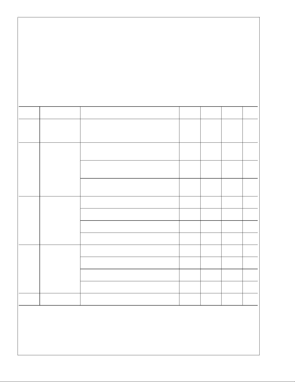
Electrical Characteristics
Typicals and limits appearing in normal type apply for TJ= 25˚C. Limits appearing in Boldface type apply over the entire junction temperature range for operation.
Symbol Parameter Conditions
V
REF
Reference Voltage LM1084-ADJ
= 10mA, VIN−V
I
OUT
10mA ≤I
OUT
≤ I
FULL LOAD
=3V
OUT
,1.5V ≤ (VIN−V
(Note 7)
V
OUT
Output Voltage
(Note 7)
LM1084-3.3
= 0mA, VIN=8V
I
OUT
0 ≤ I
OUT≤IFULL LOAD
, 4.8V≤ VIN≤15V
LM1084-5.0
= 0mA, VIN=8V
I
OUT
0 ≤ I
OUT
≤ I
FULL LOAD
, 6.5V ≤ VIN≤ 20V
LM1084-12
= 0mA, VIN= 15V
I
OUT
∆V
OUT
Line Regulation
(Note 8)
OUT
≤ I
FULL LOAD
0 ≤ I
LM1084-ADJ
=10mA, 1.5V≤ (VIN-V
I
OUT
, 13.5V ≤ VIN≤ 25V
OUT
LM1084-3.3
= 0mA, 4.8V ≤ VIN≤ 15V
I
OUT
LM1084-5.0
I
= 0mA, 6.5V ≤ VIN≤ 20V
OUT
LM1084-12
=0mA, 13.5V ≤ VIN≤ 25V
I
OUT
∆V
OUT
Load Regulation
(Note 8)
LM1084-ADJ
(V
IN-VOUT
) = 3V, 10mA ≤ I
OUT
LM1084-3.3
= 5V, 0 ≤ I
V
IN
OUT
≤ I
FULL LOAD
LM1084-5.0
= 8V, 0 ≤ I
V
IN
OUT
≤ I
FULL LOAD
LM1084-12
Dropout Voltage
(Note 9)
= 15V, 0 ≤ I
V
IN
LM1084-ADJ, 3.3, 5, 12
, ∆V
∆V
REF
OUT
OUT
= 1%, I
≤ I
FULL LOAD
=5A 1.3 1.5 V
OUT
) ≤ 15V
≤ I
FULL LOAD
OUT
) ≤ 25V
Min
(Note 6)
1.238
1.225
3.270
3.235
4.950
4.900
11.880
11.760
Typ
(Note 5)
1.250
1.250
3.300
3.300
5.000
5.000
12.000
12.000
0.015
0.035
0.5
1.0
0.5
1.0
1.0
2.0
0.1
0.2
3
7
5
10
12
24
Max
(Note 6)
1.262
1.270
3.330
3.365
5.050
5.100
12.120
12.240
0.2
0.2
6
6
10
10
25
25
0.3
0.4
15
20
20
35
36
72
Units
V
V
V
V
V
V
V
V
%
%
mV
mV
mV
mV
mV
mV
%
%
mV
mV
mV
mV
mV
mV
www.national.com3
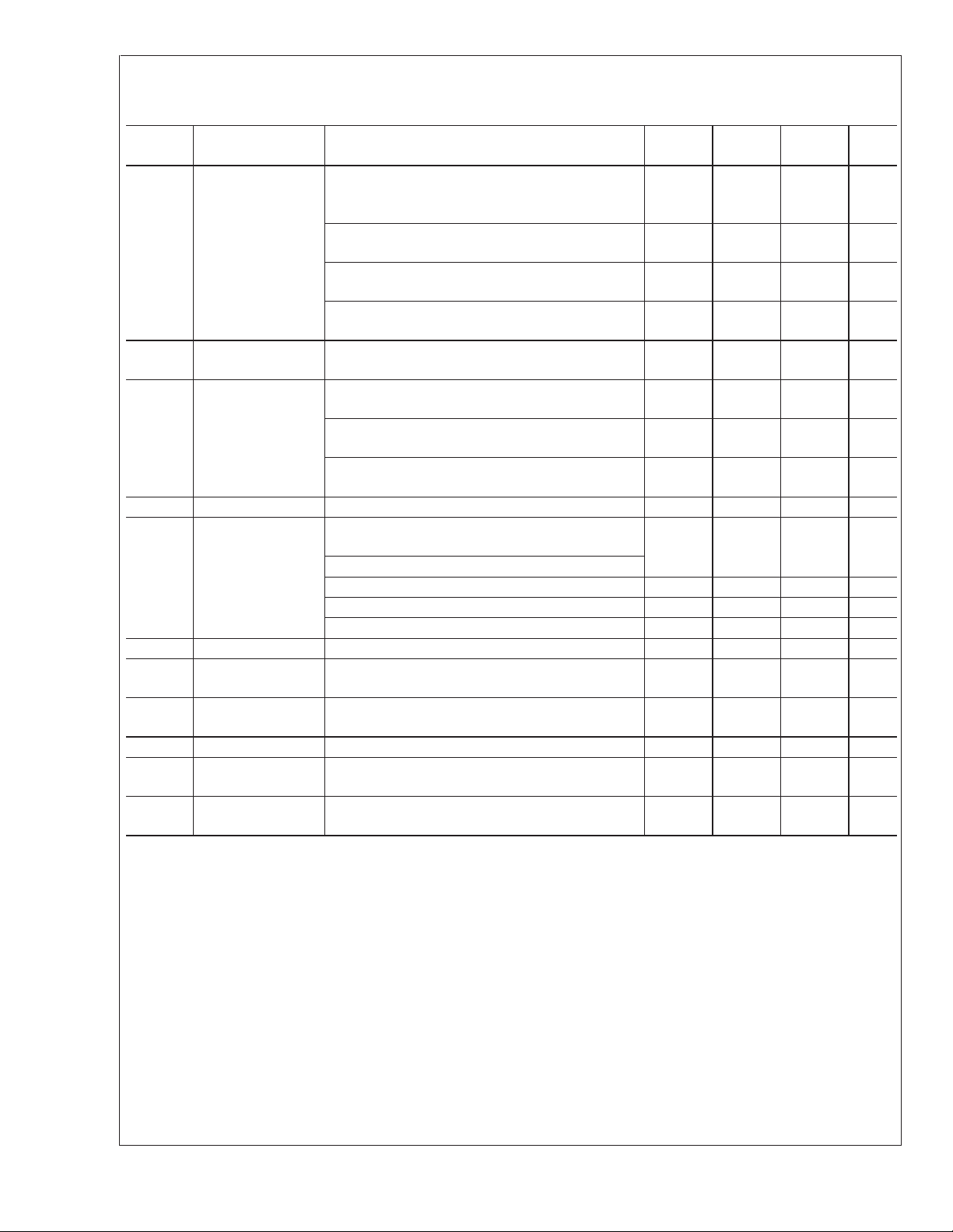
Electrical Characteristics (Continued)
Typicals and limits appearing in normal type apply for TJ= 25˚C. Limits appearing in Boldface type apply over the entire junc-
LM1084
tion temperature range for operation.
Symbol Parameter Conditions
I
LIMIT
Current Limit LM1084-ADJ
V
IN−VOUT
V
IN−VOUT
=5V
= 25V
LM1084-3.3
VIN=8V 5.5 8.0 A
LM1084-5.0
= 10V 5.5 8.0 A
V
IN
LM1084-12
VIN= 17V 5.5 8.0 A
Minimum Load
Current (Note 10)
LM1084-ADJ
V
IN−VOUT
= 25V 5 10.0 mA
Quiescent Current LM1084-3.3
VIN= 18V 5.0 10.0 mA
LM1084-5.0
≤ 20V 5.0 10.0 mA
V
IN
LM1084-12
≤ 25V 5.0 10.0 mA
V
IN
Thermal Regulation T
Ripple Rejection f
= 25˚C, 30ms Pulse 0.003 0.015 %/W
A
= 120Hz, = C
RIPPLE
=5A
I
OUT
LM1084-3.3, V
LM1084-5.0, V
LM1084-12 V
ADJ
= 6.3V 60 72 dB
IN
=8V 60 68 dB
IN
= 15V 54 60 dB
IN
= 25µF Tantalum,
OUT
, = 25µF, (VIN−VO)=3V
Adjust Pin Current LM1084 55 120 µA
Adjust Pin Current
Change
10mA ≤ I
1.5V ≤ V
≤ I
OUT
IN−VOUT
FULL LOAD
≤ 25V
,
Temperature
Stability
Long Term Stability T
RMS Output Noise
(% of V
OUT
)
Thermal Resistance
Junction-to-Case
=125˚C, 1000Hrs 0.3 1.0 %
A
10Hz ≤ f≤ 10kHz 0.003 %
3-Lead TO-263: Control Section/Output Section
3-Lead TO-220: Control Section/Output Section
Min
(Note 6)
5.5
0.3
60 75 dBLM1084-ADJ, C
Typ
(Note 5)
(Note 6)
8.0
0.6
0.2 5 µA
0.5 %
0.65/2.7
0.65/2.7
Max
Units
A
A
˚C/W
˚C/W
Note 1: Absolute Maximum Ratings indicate limits beyond which damage to the device may occur. Operating Ratings indicate conditions for which the device is
intended to be functional, but specific performance is not guaranteed. For guaranteed specifications and the test conditions, see the Electrical Characteristics.
Note 2: Power dissipation is kept in a safe range by current limiting circuitry. Refer to Overload Recovery in Application Notes.
Note 3: The maximum power dissipation is a function of T
is P
=(T
D
J(max)–TA
Note 4: For testing purposes, ESD was applied using human body model, 1.5kΩ in series with 100pF.
Note 5: Typical Values represent the most likely parametric norm.
Note 6: All limits are guaranteed by testing or statistical analysis.
Note 7: I
FULLLOAD
dissipation for the LM1084 is only achievable over a limited range of input-to-output voltage.
Note 8: Load and line regulation are measured at constant junction temperature, and are guaranteed up to the maximum power dissipation of 30W. Power
dissipation is determined by the input/output differential and the output current. Guaranteed maximum power dissipation will not be available over the full input/output
range.
Note 9: Dropout voltage is specified over the full output current range of the device.
Note 10: The minimum output current required to maintain regulation.
www.national.com 4
)/θJA. All numbers apply for packages soldered directly into a PC board. Refer to Thermal Considerations in the Application Notes.
is defined in the current limit curves. The I
, θJA, and TA. The maximum allowable power dissipation at any ambient temperature
J(max)
Curve defines the current limit as a function of input-to-output voltage. Note that 30W power
FULLLOAD
 Loading...