

查询LM104供应商
LM104/LM204/LM304 Negative Regulator
General Description
The LM104 series are precision voltage regulators which
can be programmed by a single external resistor to supply
any voltage from 40V down to zero while operating from a
single unregulated supply. They can also provide 0.01-percent regulation in circuits using a separate, floating bias
supply, where the output voltage is limited only by the
breakdown of external pass transistors. Although designed
primarily as linear, series regulators, the circuits can be used
as switching regulators, current regulators or in a number of
other control applications. Typical performance characteristics are:
Y
Subsurface zener reference
Y
1 mV regulation no load to full load
Y
0.01%/V line regulation
Y
0.2 mV/V ripple rejection
Y
0.3% temperature stability over military temperature
range
March 1989
The LM104 series is the complement of the LM105 positive
regulator, intended for systems requiring regulated negative
voltages which have a common ground with the unregulated
supply. By themselves, they can deliver output currents to
25 mA, but external transistors can be added to get any
desired current. The output voltage is set by external resistors, and either constant or foldback current limiting is made
available.
The LM104 is specified for operation over the
a
125§C military temperature range. The LM204 is specified
for operation over the
The LM304 is specified for operation from 0
b
25§Ctoa85§C temperature range.
b
55§Cto
Ctoa70§C.
§
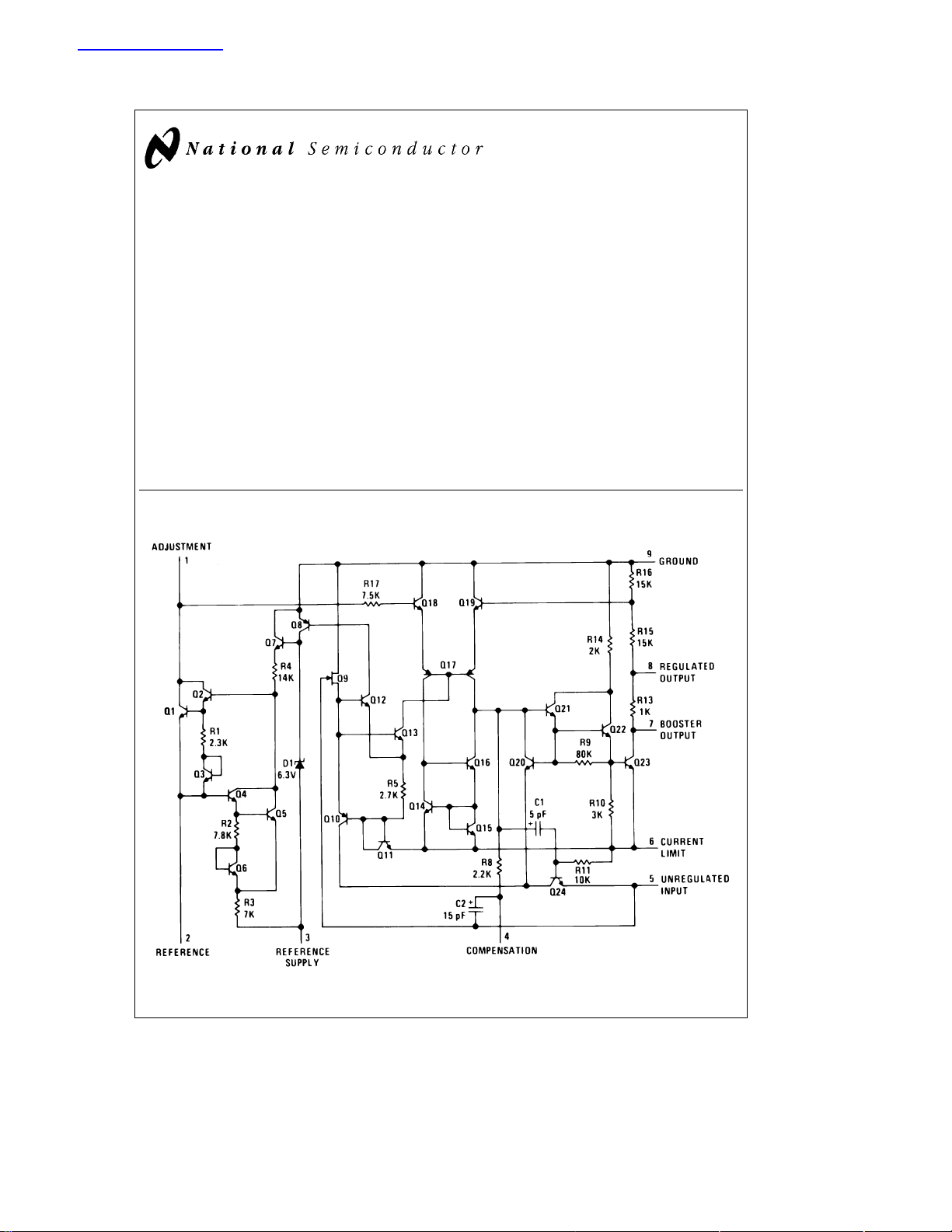
LM104/LM204/LM304 Negative Regulator
Schematic Diagram
TL/H/7754– 1
C
1995 National Semiconductor Corporation RRD-B30M115/Printed in U. S. A.
TL/H/7754
Absolute Maximum Ratings
If Military/Aerospace specified devices are required, please contact the National Semiconductor Sales Office/
Distributors for availability and specifications.
(Note 6)
LM104/LM204 LM304
Input Voltage 50V 40V
Input-Output Voltage Differential 50V 40V
Power Dissipation (Note 1) 500 mW 500 mW
Operating Temperature Range
LM104
LM204
LM304 0
Storage Temperature Range
Lead Temperature (Soldering, 10 sec.) 260
b
55§Ctoa125§C
b
25§Ctoa85§C
b
65§Ctoa150§C
C for plastic 300§C for hermetic
§
Ctoa70§C
§
b
65§Ctoa150§C
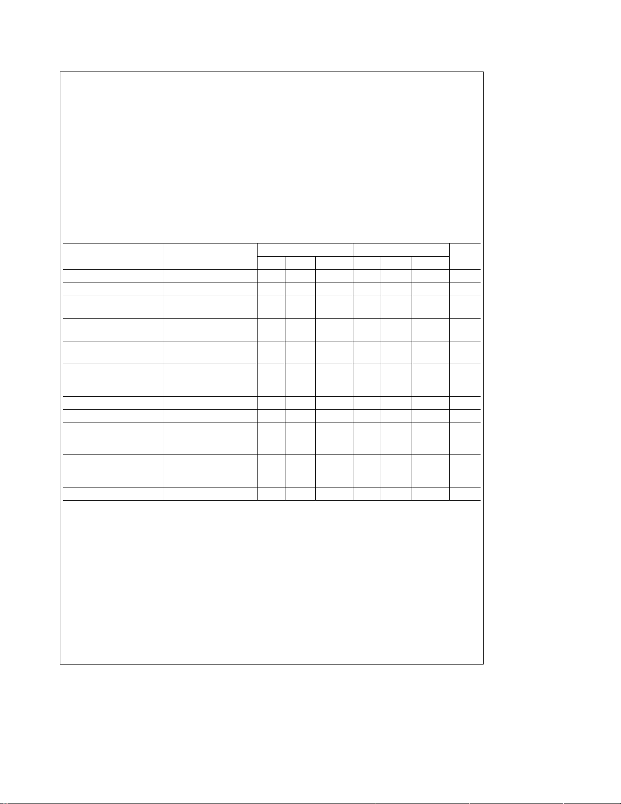
Electrical Characteristics
Parameter Conditions
Input Voltage Range
Output Voltage Range
Output-Input Voltage I
Differential (Note 3) I
Load Regulation (Note 4) OsI
Line Regulation (Note 5) V
Ripple Rejection C
Output Voltage Scale Factor R
Temperature Stability V
e
20 mA 2.0 50 2.0 40 V
O
e
5 mA 0.5 50 0.5 40 V
O
s
20 mA
O
e
R
15X 15 15mV
SC
s
b
5V
OUT
e
DV
0.1 V
19
V
IN
b
2-3
O
IN
7VtV
s
IN
e
10 mF, fe120 Hz
k
b
15V 0.2 0,.5 0.2 0.5 mV/V
t
b
15V 0.5 1.0 0.5 1.0 mV/V
IN
e
2.4k 1.8 2.0 2.2 1.8 2.0 2.2 V/kX
b
1V 0.3 1.0 0.3 1.0 %
Output Noise Voltage 10 Hzsfs10 kHz
s
b
V
O
Standby Current Drain I
Long Term Stability V
Note 1: The maximum junction temperature of the LM104 is 150§C, while that of the LM204 is 125§C and LM304 is 100§C. For operating at elevated temperatures,
devices in the H10C package must be derated based on a thermal resistance of 150
Note 2: These specifications apply for junction temperatures between
LM304) and for input and output voltages within the ranges given, unless otherwise specified. The load and line regulation specifications are for constant junction
temperature. Temperature drift effects must be taken into account separately when the unit is operating under conditions of high dissipation.
Note 3: When external booster transistors are used, the minimum output-input voltage differential is increased, in the worst case, by approximately 1V.
Note 4: The output currents given, as well as the load regulation, can be increased by the addition of external transistors. The improvement factor will be roughly
equal to the composite current gain of the added transistors.
Note 5: With zero output, the dc line regulation is determined from the ripple rejection. Hence, with output voltages between 0V and
determined from the ripple rejection, must be added to find the worst-case line regulation.
Note 6: Refer to RETS104X drawing for military specifications for the LM104.
L
e
O
5 mA, V
s
b
e
5V, C
0 0.007 0.007 %
1-9
e
C
10 mF15 15 mV
1-9
e
0 1.7 2.5 1.7 2.5 mA
O
eb
V
30V 3.6 5.0 mA
O
eb
V
40V 3.6 5.0 mA
O
1V 0.01 1.0 0.01 1.0 %
b
LM104/LM204 LM304
Units
Min Typ Max Min Typ Max
b
50
b
40
b
8
b
0.015b30
b
40
b
8V
b
0.035 V
0.056 0.1 0.056 0.1 %
C/W, junction to ambient, or 45§C/W, junction to case.
§
55§C and 150§C (betweenb25§C and 100§C for the LM204 and 0§Ctoa85§C for the
b
5V, a dc output variation,
2

Typical Performance Characteristics
Load Regulation Load Regulation Current Limiting
Supply Voltage Rejection Preregulated Reference Supply
Current Limit Sense Voltage Regulator Dropout Voltage Minimum Input Voltage
Line Transient Response Load Transient Response Standby Current Drain
Supply Voltage Rejection With
Ripple Rejection
TL/H/7754– 7
3

Connection Diagram
Metal Can Package
Typical Applications
Operating with Separate Bias Supply
High Current Regulator
Note: Pin 5 connected to case.
Top View
Order Number LM104H, LM204H or LM304H
See NS Package H10C
Basic Regulator Circuit
²
²
Solid Tantalum
TL/H/7754– 3
Solid Tantalum TL/H/7754– 5
Trim R1 for exact scale factor.
TL/H/7754– 2
Switching Regulator
²
Solid Tantalum TL/H/7754– 4
²
Solid Tantalum TL/H/7754– 6
*60 turnsÝ20 on Arnold Engineering A930157-2 Molybdenum Permalloy Core.
4

5

Physical Dimensions inches (millimeters)
LM104/LM204/LM304 Negative Regulator
Order Number LM104H, LM204H or LM304H
Metal Can Package (H)
NS Package Number H10C
LIFE SUPPORT POLICY
NATIONAL’S PRODUCTS ARE NOT AUTHORIZED FOR USE AS CRITICAL COMPONENTS IN LIFE SUPPORT
DEVICES OR SYSTEMS WITHOUT THE EXPRESS WRITTEN APPROVAL OF THE PRESIDENT OF NATIONAL
SEMICONDUCTOR CORPORATION. As used herein:
1. Life support devices or systems are devices or 2. A critical component is any component of a life
systems which, (a) are intended for surgical implant support device or system whose failure to perform can
into the body, or (b) support or sustain life, and whose be reasonably expected to cause the failure of the life
failure to perform, when properly used in accordance support device or system, or to affect its safety or
with instructions for use provided in the labeling, can effectiveness.
be reasonably expected to result in a significant injury
to the user.
National Semiconductor National Semiconductor National Semiconductor National Semiconductor
Corporation Europe Hong Kong Ltd. Japan Ltd.
1111 West Bardin Road Fax: (
Arlington, TX 76017 Email: cnjwge@tevm2.nsc.com Ocean Centre, 5 Canton Rd. Fax: 81-043-299-2408
Tel: 1(800) 272-9959 Deutsch Tel: (
Fax: 1(800) 737-7018 English Tel: (
National does not assume any responsibility for use of any circuitry described, no circuit patent licenses are implied and National reserves the right at any time without notice to change said circuitry and specifications.
Fran3ais Tel: (
Italiano Tel: (
a
49) 0-180-530 85 86 13th Floor, Straight Block, Tel: 81-043-299-2309
a
49) 0-180-530 85 85 Tsimshatsui, Kowloon
a
49) 0-180-532 78 32 Hong Kong
a
49) 0-180-532 93 58 Tel: (852) 2737-1600
a
49) 0-180-534 16 80 Fax: (852) 2736-9960
 Loading...