

PRELIMINARY
FPD87352CXA
+3.3V TFT-LCD Timing Controller with Single LVDS
July 2004
FPD87352CXA +3.3V TFT-LCD Timing Controller with Single LVDS Input/Dual RSDS Outputs
Including RTC (Response Time Compensation) for TFT-LCD Monitors and TV (XGA/WXGA/HDTV
I,II,-)
Input/Dual RSDS
™
Outputs Including RTC (Response
Time Compensation) for TFT-LCD Monitors and TV
(XGA/WXGA/HDTV I,II,-)
General Description
The FPD87352CXA is an integrated FPD-Link™+ RSDS +
TFT-LCD Timing Controller. The logic architecture is implemented using standard and default timing controller functionality based on an Embedded Gate Array. The device is
reconfigurable to the needs of a specific application by providing user-defined specifications or customer supplied
VHDL/Verilog code.
The FPD87352CXA is an ideal Timing Controller for LCD TV
Applications. It has a unique feature, RTC that will improve
the intra-gray level response time of a LCD TV panel. Improving the intra-gray level response time of the LCD panel
will result in a dramatically improved Motion Picture Image
Quality of video content that are displayed on the LCD panel.
The RTC feature is accomplished through application of a
Boost or Overdrive Voltage that will force the LC material to
respond more rapidly. This Boost or Overdrive is accomplished through combination of an internal or external EEPROM LUT (Look Up Table), which contains the boost/
overdrive levels, and external memory that acts as a Frame
Buffer.
The FPD87352CXA is a timing controller that combines an
LVDS single pixel input interface with National’s Reduced
Swing Differential Signaling (RSDS) output column driver
interface for XGA/WXGA/HDTV I,II,- resolutions. It resides
on the Flat Panel Display and provides the data buffering
and control signal generation. FPD-Link, a lower dynamic
power, low EMI (Electro Magnetic Interference) interface is
used between this timing controller and the host system. A
RSDS interface is used between the timing controller and
the column drivers.
The dual 13/10 pair differential bus conveys up to 24-bit
color data for XGA, WXGA and HDTV panels.
Features
n Input frequency range from 30 MHz to 95 MHz
n Support display resolutions XGA (1024x768), WXGA
(1280x768), HDTV I (1280x768), HDTV II (1366x768)
and HDTV - (1280x800)
n Embedded gate array for custom panel timing
n LVDS single pixel input (8-bit/6-bit) interface (FPD-Link)
n RSDS dual bus output (8-bit/6-bit)
n Drives RSDS column drivers up to 47.5 MHz clock
n Flexible RSDS data output mapping for Bottom or Top
mount
n RTC (Response time compensation) function
n 2 Wired Serial EEPROM Interface support (RTC LUT)
n Interface with external frame memory
n Virtual 8-bit color depth in FRC/Dithering mode
n Supports Graphics Controllers with spread spectrum
interface for lower EMI
n Supports external Spread Spectrum (SSCG)
n DE only mode
n CMOS circuitry operates from 3.0V–3.6V; 0˚C–70˚C
n 176 LQFP package with body size 24 mm x 24 mm x
1.4 mm, 0.5 mm pitch
RSDS™is a trademark of National Semiconductor Corporation.
© 2004 National Semiconductor Corporation DS201162 www.national.com
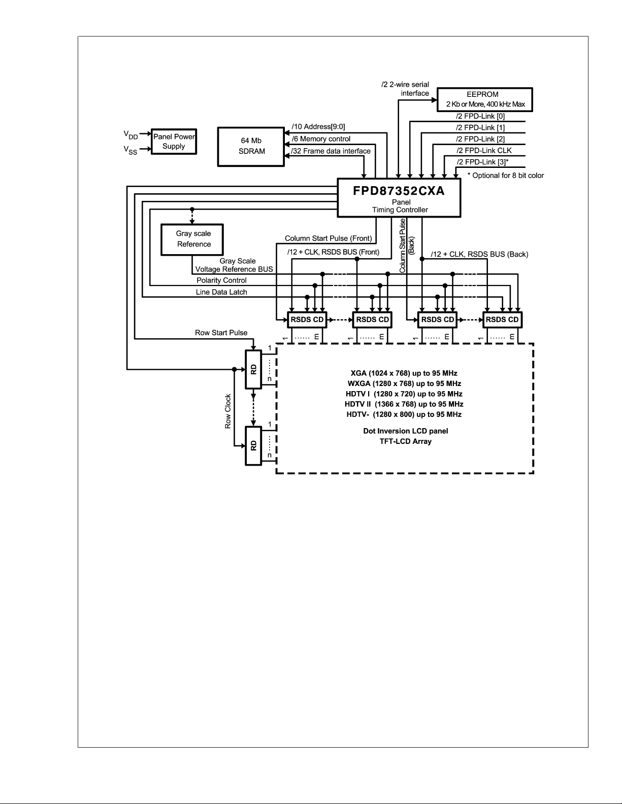
System Diagram
FPD87352CXA
FIGURE 1. Block Diagram of the LCD Module
www.national.com 2
20116201

Block Diagram
FPD87352CXA
FIGURE 2. Block Diagram
Function Description
FPD-LINK RECEIVER
The LVDS based FPD-Link Receiver receives input video
data and control timing. Four LVDS channels plus clock
provide 24-bit color.
RESETN initializes the chip with the default register values
for the LUT values from internal ROM or external EEPROM.
SSC (SPREAD SPECTRUM CONTROL)
This SSC function provides a means for reducing EMI. This
feature uses external SSC signal source that provides synchronized spread spectrum for RSDS and control signal
outputs.
2-WIRE SERIAL EEPROM INTERFACE
The Serial EEPROM Interface controls the FPD87352CXA
initialization of LUT register. If the EEPROM is not present,
the LUT value is provided by internal ROM of
FPD87352CXA.
CLK & DATA SYNCHRONIZER
This function delays and aligns data to match the internal
data process which included RSDS skew control by
RSKEW[2:0]. All the data processes are needed to be
aligned each data path through RSDS output and LCD timing control signal.
20116202
LUT REGISTER
This block provides the RTC reference values to be processed on the RTC Data Processor Block. The setting of
RTC reference values is provided by the external EEPROM
in normal condition. If the external EEPROM is not present it
will use the internal ROM’s RTC reference values. The RTC
reference values are the new gray values depending on the
difference between the current frames’ RGB gray data and
the previous frame’s RGB gray data of same pixel.
RTC DATA PROCESSOR
This function generates new gray values depending on the
difference of the current RGB gray data and same pixel of
the previous frame. The reference values fetch from the LUT
(Look Up Table) values in the LUT Register.
RSDS INTERFACE WITH SKEW CONTROL
This functional block transforms CMOS level signal to RSDS
for the system clock (DCLK) and RGB color data. The RSDS
skew is controlled by RSKEW[2:0] with delay steps between
the RSF/BCKP/N and RSF/BR/G/B[3:0]P/N which is implemented in CLK & Data synchronizer.
www.national.com3

Function Description (Continued)
VERTICAL & HORIZONTAL LCD TIMING CONTROL
This function block generates the TTL(CMOS) level signal
for the interface of column drivers and row drivers in the LCD
FPD87352CXA
system. All signals are synchronized by RSF/BCKP/N which
is RSDS data clock for the column drivers. The clock skew
control must not change the typical timing of TTL(CMOS)
level signals.
www.national.com 4

Physical Dimensions inches (millimeters) unless otherwise noted
FPD87352CXA +3.3V TFT-LCD Timing Controller with Single LVDS Input/Dual RSDS Outputs
Including RTC (Response Time Compensation) for TFT-LCD Monitors and TV (XGA/WXGA/HDTV
I,II,-)
NOTES: UNLESS OTHERWISE SPECIFIED
1. STANDARD LEAD FINISH:
7.62 MICROMETERS MINIMUM SOLDER PLATING (85/15) THICKNESS ON COPPER.
2. DIMENSION DOES NOT INCLUDE MOLD PROTRUSION. MAXIMUM ALLOWABLE MOLD PROTRUSION 0.25 mm PER
SIDE.
3. REFERENCE JEDEC REGISTRATION MS-026, VARIATION BGA, DATED FEBRUARY 1999.
Plastic Quad Flatpack, JEDEC
NS Package Number VPC176A
LIFE SUPPORT POLICY
NATIONAL’S PRODUCTS ARE NOT AUTHORIZED FOR USE AS CRITICAL COMPONENTS IN LIFE SUPPORT
DEVICES OR SYSTEMS WITHOUT THE EXPRESS WRITTEN APPROVAL OF THE PRESIDENT AND GENERAL
COUNSEL OF NATIONAL SEMICONDUCTOR CORPORATION. As used herein:
1. Life support devices or systems are devices or
systems which, (a) are intended for surgical implant
into the body, or (b) support or sustain life, and
whose failure to perform when properly used in
accordance with instructions for use provided in the
2. A critical component is any component of a life
support device or system whose failure to perform
can be reasonably expected to cause the failure of
the life support device or system, or to affect its
safety or effectiveness.
labeling, can be reasonably expected to result in a
significant injury to the user.
BANNED SUBSTANCE COMPLIANCE
National Semiconductor certifies that the products and packing materials meet the provisions of the Customer Products
Stewardship Specification (CSP-9-111C2) and the Banned Substances and Materials of Interest Specification
(CSP-9-111S2) and contain no ‘‘Banned Substances’’ as defined in CSP-9-111S2.
National Semiconductor
Americas Customer
Support Center
Email: new.feedback@nsc.com
Tel: 1-800-272-9959
www.national.com
National does not assume any responsibility for use of any circuitry described, no circuit patent licenses are implied and National reserves the right at any time without notice to change said circuitry and specifications.
National Semiconductor
Europe Customer Support Center
Fax: +49 (0) 180-530 85 86
Email: europe.support@nsc.com
Deutsch Tel: +49 (0) 69 9508 6208
English Tel: +44 (0) 870 24 0 2171
Français Tel: +33 (0) 1 41 91 8790
National Semiconductor
Asia Pacific Customer
Support Center
Email: ap.support@nsc.com
National Semiconductor
Japan Customer Support Center
Fax: 81-3-5639-7507
Email: jpn.feedback@nsc.com
Tel: 81-3-5639-7560
 Loading...