

Page 1
FPN530
FPN530A
FPN530 / FPN530A
C
B
E
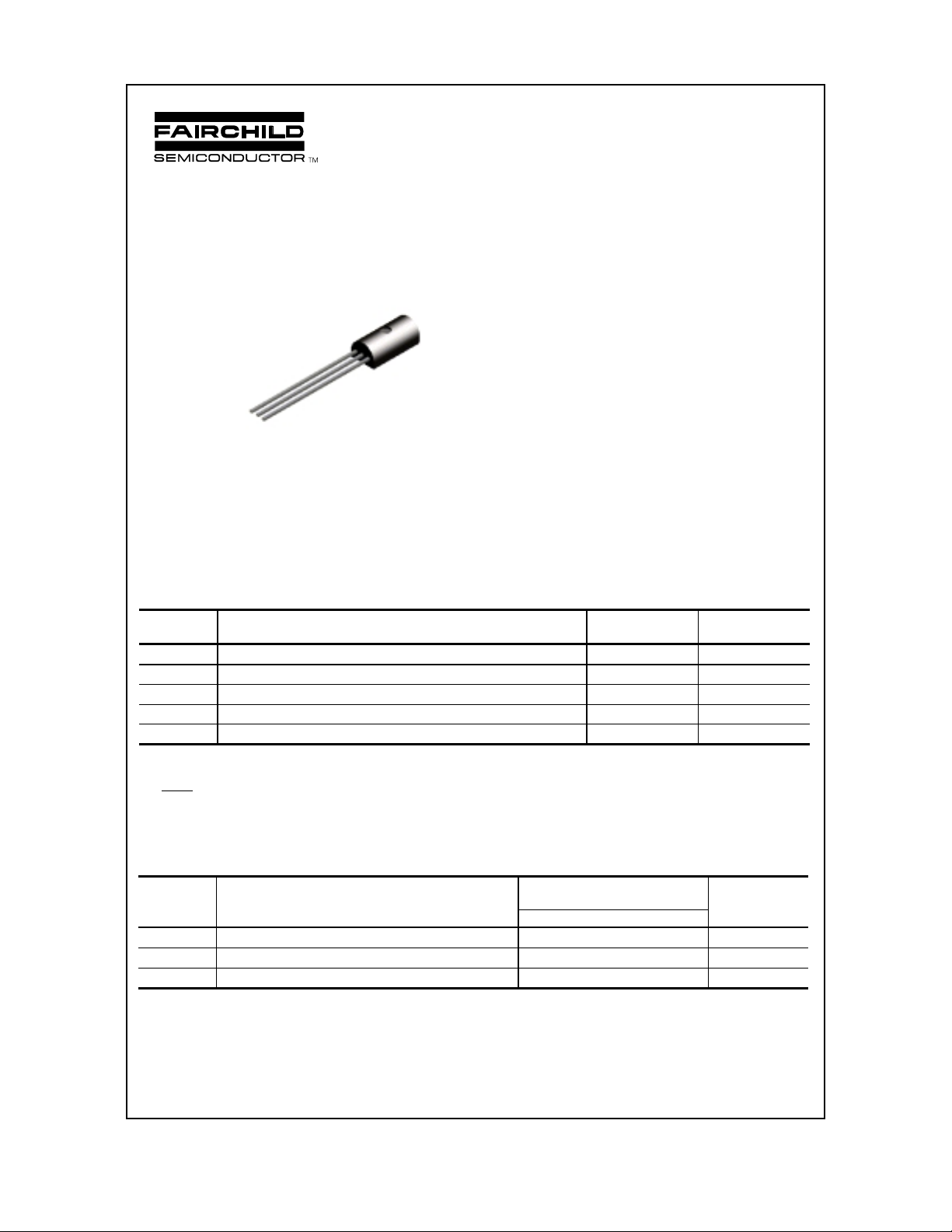
TO-226
NPN Low Saturation Transistor
These devices are designed for high current gain and low
saturation voltage with collector currents up to 3.0 A continuous.
Sourced from Process NC.
Absolute Maximum Ratings* TA = 25°C unless otherwise noted
Symbol Parameter Value Units
V
CEO
V
CBO
V
EBO
I
C
TJ, T
stg
*These ratings are limiting values above which the serviceability of any semiconductor device may be impaired.
NOTES:
1) These ratings are based on a maximum junction temperature of 150 degrees C.
2) These are steady state limits. The factory should be consulted on applications involving pulsed or low duty cycle operations.
Thermal Characteristics TA = 25°C unless otherwise noted
Collector-Emitter V ol tage 30 V
Collector-Base Voltage 60 V
Emitter-Base Volt age 5.0 V
Collector Current - Continuous 3.0 A
Operating and Storage Junction Temperature Range -55 to +150
C
°
Symbol Characteristic Max Units
FPN530 / FPN530A
P
D
R
θ
JC
R
θ
JA
1999 Fairchild Semiconductor Corporation
Total Device Dissipation 1.0 W
Thermal Resistance, Junction to Case 50
Thermal Resistance, Junction to Ambient 125
°C/W
°C/W
Page 2
NPN Low Saturation Transistor
(continued)
Electrical Characteristics TA = 25°C unless otherwise noted
Symbol Parameter Test Conditions Min Max Units
OFF CHARACTERISTICS
BV
CEO
BV
CBO
BV
EBO
I
CBO
I
EBO
ON CHARACTERISTICS*
h
FE
V
sat
CE(
V
sat
BE(
V
BE(on)
Collector-Emitter Breakdown
IC = 10 mA, IB = 0 30 V
Voltage
Collector-Base Breakdown Voltage
Emitter-Base Breakdown Voltage
Collector Cutoff Current VCB = 30 V, I
Emitter Cutoff Current VEB = 4.0 V, I
DC Current Gain
Collector-Emitter S aturation Voltage
)
I
= 100 µA, IE = 0
C
I
= 100 µA, IC = 0
E
= 0
E
= 30 V, I
V
CB
= 100 mA, VCE = 2.0 V
I
C
I
= 1.0 A, VCE = 2.0 V
C
= 2.0 A, VCE = 2.0 V
I
C
= 1.0 A, IB = 100 mA
I
C
= 0, TA = 100°C
E
= 0 100 nA
C
530
530A
530
60 V
5.0 V
100
250
120
80
530A
I
= 2.0 A, IB = 200 mA
Base-Emitter Saturation Voltage IC = 1.0 A, IB = 100 mA 1.25 V
)
C
Base-Emitter Saturation Voltage IC = 1.0 A, VCE = 2.0 V 1.0 V
100
10
300
250
450
nA
µ
mV
mV
mV
A
FPN530 / FPN530A
SMALL SIGNAL CHARACTERISTICS
C
obo
F
T
Output Capacitance VCB = 10 V, IE = 0, f = 1.0 MHz 50 pF
Transition Frequency IC = 100 mA, VCE = 5.0 V,
*Pulse T est: Pulse Width ≤ 300 µs, Duty Cycle ≤ 2.0%
f = 100 MHz
150 MHz
Page 3

T ypical Characteristics
FPN530 / FPN530A
NPN Low Saturation Transistor
(continued)
Base-Emitt er Sat urat ion
Voltage vs Collector Current
1.6
β = 10
1.4
1.2
1
0.8
0.6
0.4
0.2
0.001 0.01 0.1 1 10
BESAT
V -BASE-EMITTER SATURATION VOLTAGE(V)
- 40 °C
125 °C
I - COLLECTO R CURR ENT ( A)
C
25 °C
Collector-Emitter Sat urati on
Voltage vs Collector Current
0.8
β = 10
0.6
0.4
0.2
0
0.001 0.01 0.1 1 10
CESAT
V - COLL ECTO R -EMITTER VOL TA GE (V)
I - COLLEC T OR CU R RENT ( A)
C
125 °C
- 40°C
25°C
Ba se -E m i t ter On Volt a g e v s
Collector Current
1.4
V = 2.0V
ce
1.2
1
0.8
0.6
0.4
0.2
BEON
0.0001 0.001 0.01 0.1 1 10
V - BASE-EMIT TER O N VOLTAGE (V)
I - COLLECTOR CURRENT (A)
C
- 40 °C
25 °C
125 °C
Inpu t /Ou tput Capacitance vs
Reverse Bia s Voltage
450
400
350
300
250
200
150
CAPACITANCE (pf)
100
50
0
0.1 0.5 1 10 20 50 100
C
ibo
C
obo
V - COLLECTOR VOLTAGE (V)
CE
f = 1.0MH z
Current Gain vs Collector Curren t
800
V = 2.0V
ce
700
600
500
400
300
FE
200
H - CURRENT GAIN
100
0
0.0001 0.001 0.01 0.1 1 10
125 °C
25°C
- 40°C
I - COLLE CTO R CU RRENT (A)
C
Power Dissipation vs
Ambient Tem peratur e
1
0.75
0.5
0.25
D
P - POWER DISSIPATION (W)
0
0 25 50 75 100 125 150
TO-226
TEM P E RAT U RE ( C)
°
Page 4

TRADEMARKS
The following are registered and unregistered trademarks Fairchild Semiconductor owns or is authorized to use and is
not intended to be an exhaustive list of all such trademarks.
ACEx™
Bottomless™
CoolFET™
CROSSVOLT™
DOME™
E2CMOS
EnSigna
TM
TM
FACT™
FACT Quiet Series™
FAST
FASTr™
GlobalOptoisolator™
GTO™
HiSeC™
ISOPLANAR™
MICROWIRE™
OPTOLOGIC™
OPTOPLANAR™
P ACMAN™
POP™
PowerTrench
QFET™
QS™
QT Optoelectronics™
Quiet Series™
SILENT SWITCHER
SMART ST ART™
SuperSOT™-3
SuperSOT™-6
SuperSOT™-8
SyncFET™
TinyLogic™
UHC™
VCX™
DISCLAIMER
FAIRCHILD SEMICONDUCTOR RESERVES THE RIGHT TO MAKE CHANGES WITHOUT FURTHER
NOTICE TO ANY PRODUCTS HEREIN T O IMPROVE RELIABILITY , FUNCTION OR DESIGN. FAIRCHILD
DOES NOT ASSUME ANY LIABILITY ARISING OUT OF THE APPLICA TION OR USE OF ANY PRODUCT
OR CIRCUIT DESCRIBED HEREIN; NEITHER DOES IT CONVEY ANY LICENSE UNDER ITS PA TENT
RIGHTS, NOR THE RIGHTS OF OTHERS.
LIFE SUPPORT POLICY
FAIRCHILD’S PRODUCTS ARE NOT AUTHORIZED FOR USE AS CRITICAL COMPONENTS IN LIFE SUPPORT
DEVICES OR SYSTEMS WITHOUT THE EXPRESS WRITTEN APPROVAL OF FAIRCHILD SEMICONDUCTOR CORPORA TION.
As used herein:
1. Life support devices or systems are devices or
systems which, (a) are intended for surgical implant into
the body, or (b) support or sustain life, or (c) whose
failure to perform when properly used in accordance
with instructions for use provided in the labeling, can be
reasonably expected to result in significant injury to the
user.
2. A critical component is any component of a life
support device or system whose failure to perform can
be reasonably expected to cause the failure of the life
support device or system, or to affect its safety or
effectiveness.
PRODUCT STA TUS DEFINITIONS
Definition of Terms
Datasheet Identification Product Status Definition
Advance Information
Preliminary
No Identification Needed
Obsolete
Formative or
In Design
First Production
Full Production
Not In Production
This datasheet contains the design specifications for
product development. Specifications may change in
any manner without notice.
This datasheet contains preliminary data, and
supplementary data will be published at a later date.
Fairchild Semiconductor reserves the right to make
changes at any time without notice in order to improve
design.
This datasheet contains final specifications. Fairchild
Semiconductor reserves the right to make changes at
any time without notice in order to improve design.
This datasheet contains specifications on a product
that has been discontinued by Fairchild semiconductor.
The datasheet is printed for reference information only.
Rev. G
 Loading...