

DS90LV048A
3V LVDS Quad CMOS Differential Line Receiver
DS90LV048A 3V LVDS Quad CMOS Differential Line Receiver
May 2001
General Description
The DS90LV048Ais a quad CMOS flow-through differential
line receiver designed for applications requiring ultra low
power dissipation and high data rates. The device is designed to support data rates in excess of 400 Mbps (200
MHz) utilizing Low Voltage Differential Signaling (LVDS)
technology.
The DS90LV048A accepts low voltage (350 mV typical) differential input signals and translates them to 3V CMOS
output levels. The receiver supports a TRI-STATE
that may be used to multiplex outputs. The receiver also
supports open, shorted and terminated (100Ω) input failsafe. The receiver output will be HIGH for all fail-safe conditions. The DS90LV048A has a flow-through pinout for easy
PCB layout.
The EN and EN
TRI-STATE outputs. The enables are common to all four
receivers. The DS90LV048A and companion LVDS line
driver (eg. DS90LV047A) provide a new alternative to high
power PECL/ECL devices for high speedpoint-to-point interface applications.
*
inputs areANDed together and control the
®
function
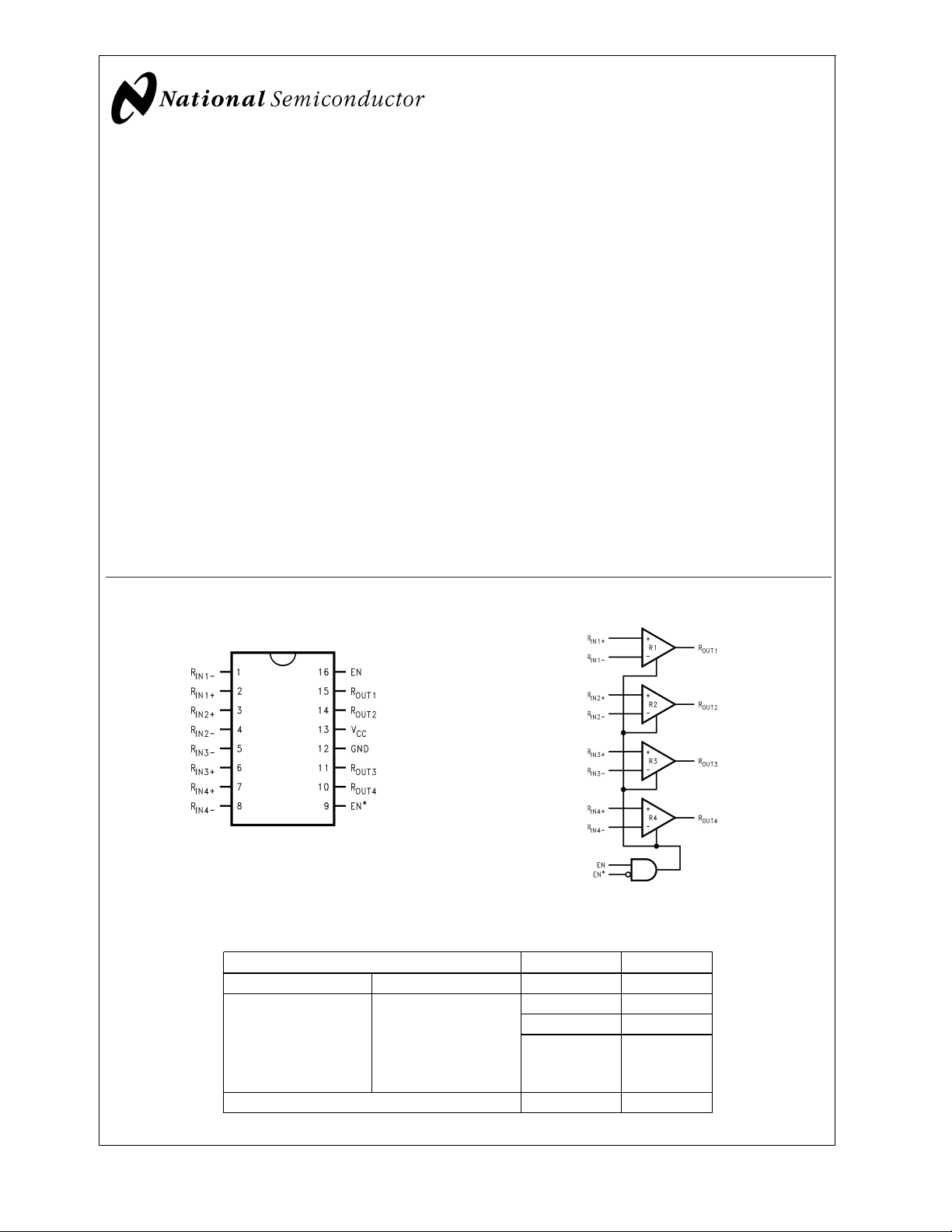
Connection Diagram
Dual-in-Line
Features
>
n
400 Mbps (200 MHz) switching rates
n Flow-through pinout simplifies PCB layout
n 150 ps channel-to-channel skew (typical)
n 100 ps differential skew (typical)
n 2.7 ns maximum propagation delay
n 3.3V power supply design
n High impedance LVDS inputs on power down
n Low Power design (40mW 3.3V static)
n Interoperable with existing 5V LVDS drivers
n Accepts small swing (350 mV typical) differential signal
levels
n Supports open, short and terminated input fail-safe
n 0V to −100mV threshold region
n Conforms to ANSI/TIA/EIA-644 Standard
n Industrial temperature operating range (-40˚C to +85˚C)
n Available in SOIC and TSSOP package
Functional Diagram
Order Number DS90LV048ATM, DS90LV048ATMTC
See NS Package Number M16A, MTC16
10088801
10088802
Truth Table
ENABLES INPUTS OUTPUT
EN EN* R
H L or Open VID≥ 0V H
All other combinations of ENABLE inputs X Z
TRI-STATE®is a registered trademark of National Semiconductor Corporation.
© 2001 National Semiconductor Corporation DS100888 www.national.com
IN+−RIN−
V
≤ −0.1V L
ID
Full Fail-safe
OPEN/SHORT
or Terminated
R
OUT
H
Absolute Maximum Ratings (Note 1)
If Military/Aerospace specified devices are required,
please contact theNational Semiconductor Sales Office/
Distributors for availability and specifications.
DS90LV048A
Supply Voltage (V
Input Voltage (R
Enable Input Voltage (EN, EN*) −0.3V to (V
Output Voltage (R
Maximum Package Power Dissipation +25˚C
M Package 1025 mW
MTC Package 866 mW
Derate M Package 8.2 mW/˚C above +25˚C
Derate MTC Package 6.9 mW/˚C above +25˚C
Storage Temperature Range −65˚C to +150˚C
) −0.3V to +4V
CC
IN+,RIN−
) −0.3V to 3.9V
) −0.3V to (VCC+ 0.3V)
OUT
CC
+ 0.3V)
(4 sec.) +260˚C
Maximum Junction
Temperature +150˚C
ESD Rating (Note 10)
(HBM, 1.5 kΩ, 100 pF) ≥ 10 kV
(EIAJ, 0 Ω, 200 pF) ≥ 1200 V
Recommended Operating
Conditions
Min Typ Max Units
Supply Voltage (V
) +3.0 +3.3 +3.6 V
CC
Receiver Input Voltage GND +3.0 V
Operating Free Air
Temperature (T
) −40 25 +85 ˚C
A
Lead Temperature Range Soldering
Electrical Characteristics
Over Supply Voltage and Operating Temperature ranges, unless otherwise specified. (Notes 2, 3)
Symbol Parameter Conditions Pin Min Typ Max Units
V
TH
V
TL
VCMR Common-Mode Voltage Range VID = 200mV pk to pk (Note 5) 0.1 2.3 V
I
IN
V
OH
V
OL
I
OS
I
OZ
V
IH
V
IL
I
I
V
CL
I
CC
I
CCZ
Differential Input High Threshold VCM= +1.2V, 0.05V, 2.95V (Note 13) R
Differential Input Low Threshold R
Input Current VIN= +2.8V VCC= 3.6V or 0V −10
V
= 0V −10
IN
V
= +3.6V VCC= 0V -20
IN
Output High Voltage IOH= −0.4 mA, VID= +200 mV R
I
= −0.4 mA, Input terminated 2.7 3.3 V
OH
I
= −0.4 mA, Input shorted 2.7 3.3 V
OH
, −35 0 mV
IN+
−100 −35 mV
IN−
±
5 +10 µA
±
1 +10 µA
±
1 +20 µA
2.7 3.3 V
OUT
Output Low Voltage IOL= 2 mA, VID= −200 mV 0.05 0.25 V
Output Short Circuit Current Enabled, V
Output TRI-STATE Current Disabled, V
Input High Voltage EN,
Input Low Voltage GND 0.8 V
Input Current VIN=0VorVCC, Other Input = VCCor GND −10
= 0V (Note 11) −15 −47 −100 mA
OUT
OUT
=0VorV
CC
−10
±
1 +10 µA
2.0 V
EN*
±
5 +10 µA
CC
Input Clamp Voltage ICL= −18 mA −1.5 −0.8 V
No Load Supply Current
EN=VCC, Inputs Open V
CC
915mA
Receivers Enabled
No Load Supply Current EN = GND, Inputs Open 1 5 mA
Receivers Disabled
V
Switching Characteristics
Over Supply Voltage and Operating Temperature ranges, unless otherwise specified. (Notes 3, 4, 7, 8)
Symbol Parameter Conditions Min Typ Max Units
t
PHLD
t
PLHD
t
SKD1
t
SKD2
Differential Propagation Delay High to Low CL= 15 pF 1.2 2.0 2.7 ns
Differential Propagation Delay Low to High VID= 200 mV 1.2 1.9 2.7 ns
Differential Pulse Skew |t
PHLD−tPLHD
Differential Channel-to-Channel Skew; same device
| (Note 6) (
Figure 1
and
Figure 2
) 0 0.1 0.4 ns
0 0.15 0.5 ns
(Note 7)
t
SKD3
t
SKD4
t
TLH
t
THL
www.national.com 2
Differential Part to Part Skew (Note 8) 1.0 ns
Differential Part to Part Skew (Note 9) 1.5 ns
Rise Time 0.5 1.0 ns
Fall Time 0.35 1.0 ns
Over Supply Voltage and Operating Temperature ranges, unless otherwise specified. (Notes 3, 4, 7, 8)
Switching Characteristics (Continued)
Symbol Parameter Conditions Min Typ Max Units
t
PHZ
t
PLZ
t
PZH
t
PZL
f
MAX
Disable Time High to Z RL=2kΩ 814ns
Disable Time Low to Z CL=15pF 8 14 ns
Enable Time Z to High (
Figure 3
and
Figure 4
) 9 14 ns
Enable Time Z to Low 914ns
Maximum Operating Frequency (Note 14) All Channels Switching 200 250 MHz
Note 1: “Absolute Maximum Ratings” are those values beyond which the safety of the device cannot be guaranteed. They are not meant to imply that the devices
should be operated at these limits. The table of “Electrical Characteristics” specifies conditions of device operation.
Note 2: Current into device pins is defined as positive. Current out of device pins is defined as negative. All voltages are referenced to ground unless otherwise
specified.
Note 3: All typicals are given for: V
Note 4: Generator waveform for all tests unless otherwise specified:f=1MHz, Z
Note 5: The VCMR range is reduced for larger VID.Example:if VID = 400mV,the VCMR is 0.2V to 2.2V.The fail-safe condition with inputs shorted is not supported
over the common-mode range of 0V to 2.4V, but is supported only with inputs shorted and no external common-mode voltage applied. A VID up to V
be applied to the R
from 200mV to 400mV. Skew specifications apply for 200mV ≤ VID ≤ 800mV over the common-mode range .
Note 6: t
Note 7: t
any event on the inputs.
Note 8: t
and within 5˚C of each other within the operating temperature range.
Note 9: t
operating temperature and voltage ranges, and across process distribution. t
Note 10: ESD Rating:HBM (1.5 kΩ, 100 pF) ≥ 10kV
EIAJ (0Ω, 200 pF) ≥ 1200V
Note 11: Output short circuit current (I
exceed maximum junction temperature specification.
Note 12: C
Note 13: V
AC specifications, the common voltage range is 0.1V to 2.3V
Note 14: f
(max 0.4V), VOH(min 2.7V), Load = 15 pF (stray plus probes).
V
OL
is the magnitude difference in differential propagation delay time between the positive going edge and the negative going edge of the same channel
SKD1
, Channel-to-Channel Skew is defined as the difference between the propagation delay of one channel and that of the others on the same chip with
SKD2
, part to part skew, is the differential channel-to-channel skew of any event between devices. This specification applies to devices at the same VCC,
SKD3
, part to part skew, is the differential channel-to-channel skew of any event between devices. This specification applies to devices over recommended
SKD4
includes probe and jig capacitance.
L
is always higher than R
CC
generator input conditions: tr=t
MAX
inputs with the Common-Mode voltage set to VCC/2. Propagation delay and Differential Pulse skew decrease when VID is increased
IN+/RIN−
= +3.3V, TA= +25˚C.
CC
) is specified as magnitude only, minus sign indicates direction only. Only one output should be shorted at a time, do not
OS
and R
IN+
voltage. R
IN−
<
1 ns (0% to 100%), 50% duty cycle, differential (1.05V to 1.35V peak to peak). Output criteria: 60/40% dutycycle,
f
IN−
and R
are allowed to have a voltage range −0.2V to VCC− VID/2. However,to be compliant with
IN+
=50Ω,trand tf(0% to 100%) ≤ 3 ns for RIN.
O
is defined as |Max−Min| differential propagation delay.
SKD4
−0Vmay
CC
DS90LV048A
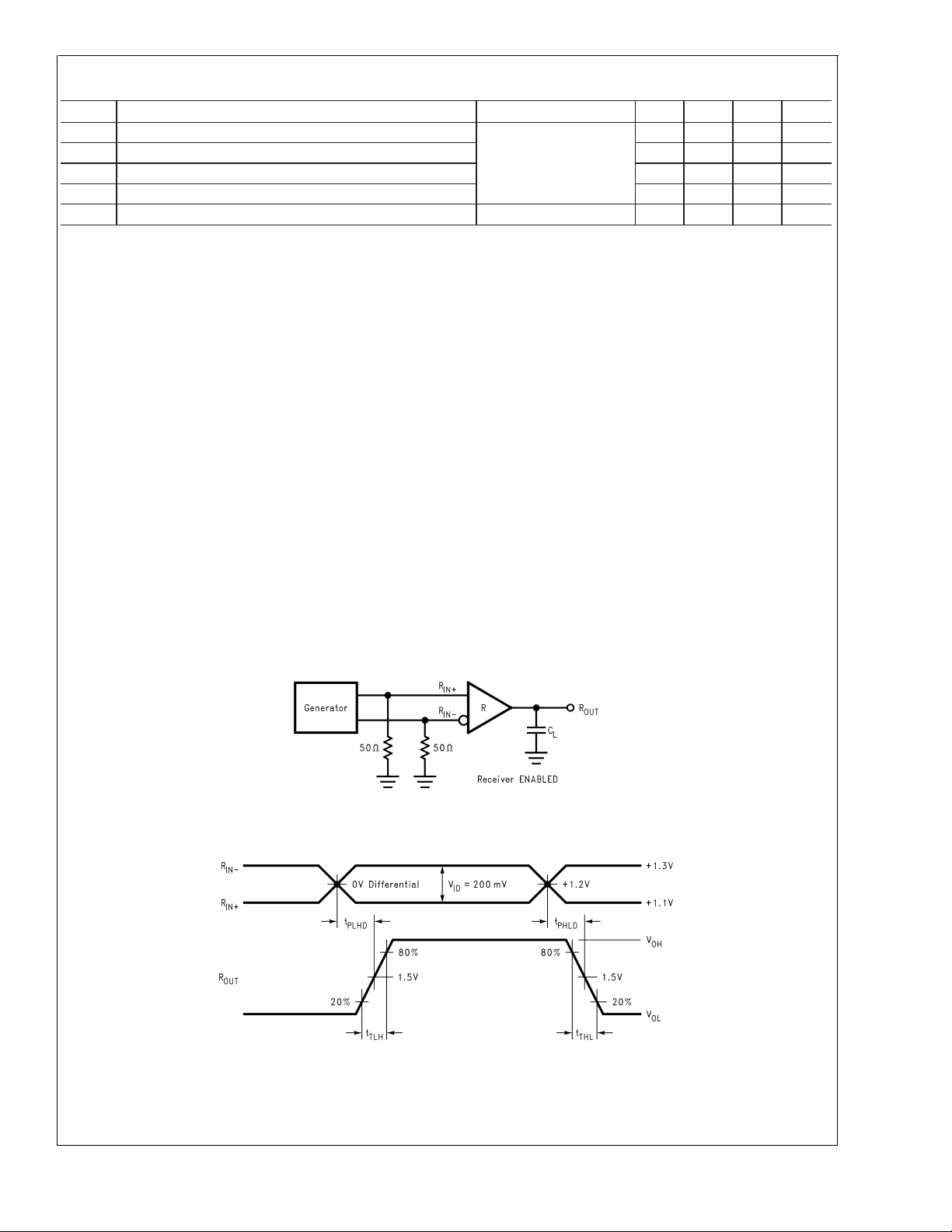
Parameter Measurement Information
FIGURE 1. Receiver Propagation Delay and Transition Time Test Circuit
FIGURE 2. Receiver Propagation Delay and Transition Time Waveforms
10088803
10088804
www.national.com3
Parameter Measurement Information (Continued)
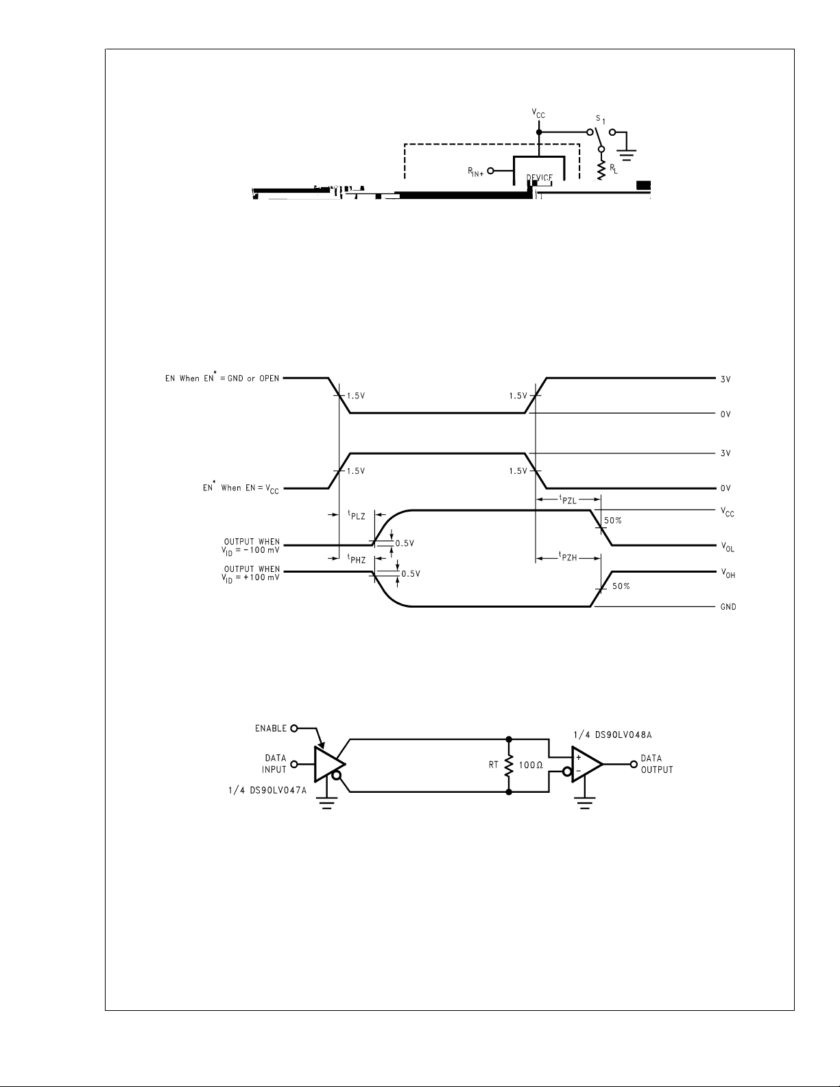
DS90LV048A
CLincludes load and test jig capacitance.
S
for t
and t
1=VCC
S
= GND for t
1
PZL
PZH
PLZ
and t
measurements.
measurements.
PHZ
10088805
FIGURE 3. Receiver TRI-STATE Delay Test Circuit
10088806
FIGURE 4. Receiver TRI-STATE Delay Waveforms
Typical Application
Balanced System
FIGURE 5. Point-to-Point Application
Applications Information
General application guidelines and hints for LVDS drivers
and receivers may be found in the following application
notes: LVDS Owner’s Manual (lit #550062-002), AN-808,
AN-977, AN-971, AN-916, AN-805, AN-903. The latest applications material is available on the web at:
www.national.com/lvds.
LVDSdriversand receivers are intendedto be primarily used
in an uncomplicated point-to-point configuration as is shown
www.national.com 4
10088807
in
Figure 5
. This configuration provides a clean signaling
environment for the fast edge rates of the drivers. The receiver is connected to the driver through a balanced media
which may be a standard twisted pair cable, a parallel pair
cable, or simply PCB traces. Typically, the characteristic
impedance of the media is in the range of 100Ω. A termination resistor of 100Ω (selected to match the media), and is
located as close to the receiver input pins as possible. The
 Loading...