

National Semiconductor DS90LV032A Technical data
DS90LV032A
3V LVDS Quad CMOS Differential Line Receiver
DS90LV032A 3V LVDS Quad CMOS Differential Line Receiver
July 1999
General Description
The DS90LV032Ais a quad CMOS differential line receiver
designed for applications requiring ultra low power dissipation and high data rates. The device is designed to support
data rates in excess of 400 Mbps (200 MHz) utilizing Low
Voltage Differential Signaling (LVDS) technology.
The DS90LV032Aaccepts low voltage (350 mV typical) differential input signals and translates them to 3V CMOS output levels. The receiver supports a TRI-STATE
may be used to multiplex outputs. The receiver also supports
open, shorted and terminated (100Ω) input Fail-safe. The receiver output will be HIGH for all fail-safe conditions.
The DS90LV032A and companion LVDS line driver (eg.
DS90LV031A) provide a new alternative to high power
PECL/ECL devices for high speed point-to-point interface
applications.
®
function that
Features
>
n
400 Mbps (200 MHz) switching rates
n 0.1 ns channel-to-channel skew (typical)
n 0.1 ns differential skew (typical)
n 3.3 ns maximum propagation delay
n 3.3V power supply design
n Power down high impedance on LVDS inputs
n Low Power design (40mW 3.3V static)
n Interoperable with existing 5V LVDS networks
n Accepts small swing (350 mV typical) VID
n Supports open, short and terminated input fail-safe
n Compatible with ANSI/TIA/EIA-644
n Industrial temp. operating range (-40˚C to +85˚C)
n Available in SOIC and TSSOP Packaging
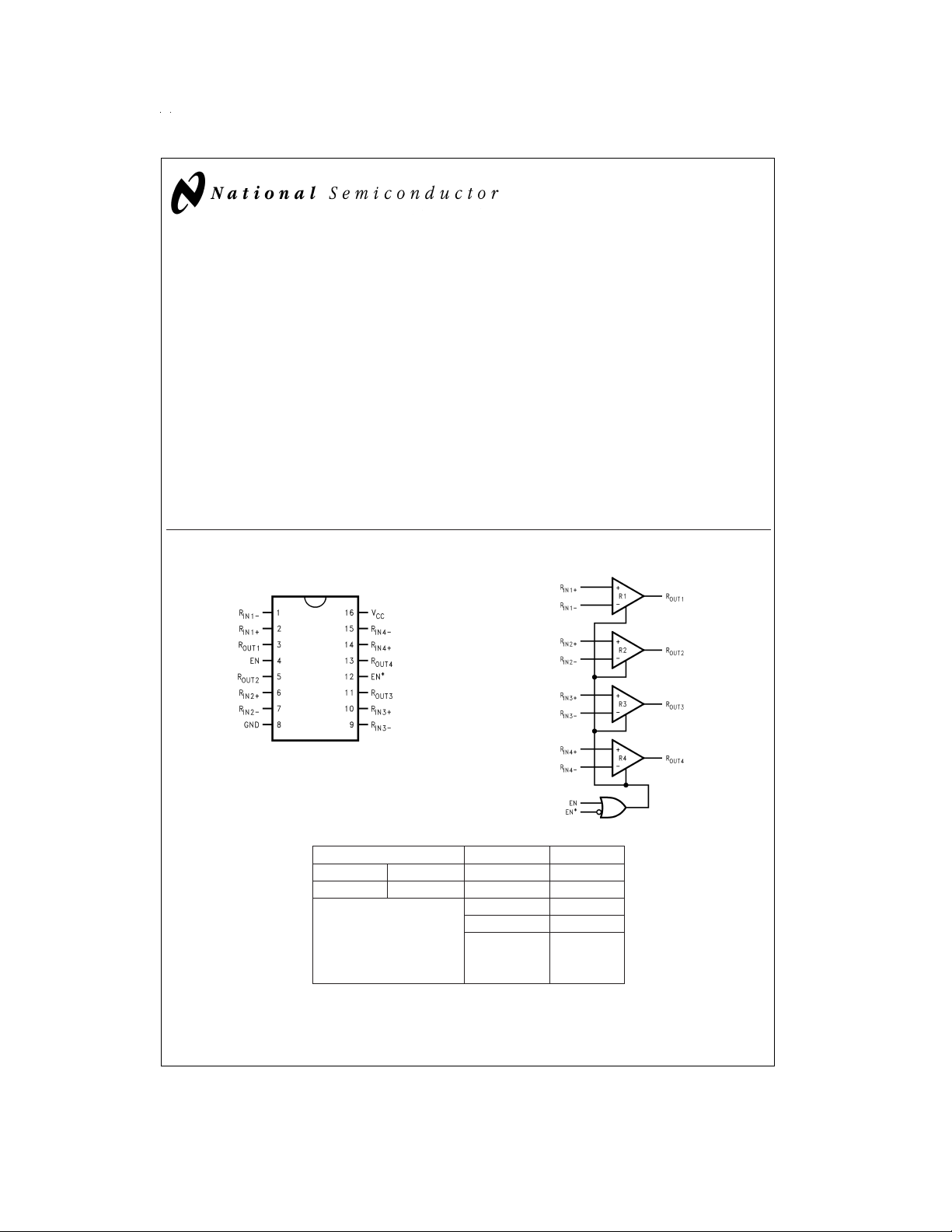
Connection Diagram Functional Diagram
Dual-in-Line
DS100067-1
Order Number DS90LV032ATM
See NS Package Number M16A or MTC16
or DS90LV032ATMTC
DS100067-2
ENABLES INPUTS OUTPUT
EN EN* R
LH X Z
All other combinations V
of ENABLE inputs V
© 1999 National Semiconductor Corporation DS100067 www.national.com
IN+−RIN−
≥ 0.1V H
ID
≤ −0.1V L
ID
Full Fail-safe
OPEN/SHORT H
or Terminated
R
OUT

Absolute Maximum Ratings (Note 1)
If Military/Aerospace specified devices are required,
please contact the National Semiconductor Sales Office/
Distributors for availability and specifications.
Supply Voltage (V
Input Voltage (R
Enable Input Voltage (EN, EN*) −0.3V to (V
Output Voltage (R
Maximum Package Power Dissipation +25˚C
M Package 1025 mW
MTC Package 866 mW
Derate M Package 8.2 mW/˚C above +25˚C
Derate MTC Package 6.9 mW/˚C above +25˚C
Storage Temperature Range −65˚C to +150˚C
) −0.3V to +4V
CC
) −0.3V to +3.9V
IN+,RIN−
) −0.3V to (VCC+ 0.3V)
OUT
CC
+ 0.3V)
(Soldering 4 sec.) +260˚C
Maximum Junction Temperature +150˚C
ESD Rating (Note 10)
(HBM 1.5 kΩ, 100 pF) ≥ 4.5 kV
(EIAJ 0 Ω, 200 pF) ≥ 250 V
Recommended Operating
Conditions
Supply Voltage (V
) +3.0 +3.3 +3.6 V
CC
Receiver Input Voltage GND +3.0 V
Operating Free Air
Temperature (T
) −40 25 +85 ˚C
A
Min Typ Max Units
Lead Temperature Range
Electrical Characteristics
Over Supply Voltage and Operating Temperature ranges, unless otherwise specified. (Note 2)
Symbol Parameter Conditions Pin Min Typ Max Units
V
V
Differential Input High Threshold VCM= +1.2V
TH
Differential Input Low Threshold −100 −20 mV
TL
(Note 13)
VCMR Common-Mode Voltage Range VID=200 mV peak to peak (Note 5) 0.1 2.3 V
I
V
V
I
I
V
V
I
V
I
Input Current VIN= +2.8V VCC= 3.6V or 0V −10
IN
Output High Voltage IOH= −0.4 mA, VID= +200 mV R
OH
Output Low Voltage IOL= 2 mA, VID= −200 mV 0.1 0.25 V
OL
Output Short Circuit Current Enabled, V
OS
Output TRI-STATE Current Disabled, V
OZ
Input High Voltage EN,
IH
Input Low Voltage GND 0.8 V
IL
Input Current VIN=0VorVCC, Other Input = VCCor
I
Input Clamp Voltage ICL= −18 mA −1.5 −0.8 V
CL
No Load Supply Current EN, EN* = VCCor GND, Inputs Open V
CC
V
= 0V −10
IN
V
= +3.6V VCC= 0V -20 +20 µA
IN
I
= −0.4 mA, Input terminated 2.7 3.0 V
OH
I
= −0.4 mA, Input shorted 2.7 3.0 V
OH
= 0V (Note 11) −15 −48 −120 mA
OUT
=0VorV
OUT
CC
GND
Receivers Enabled EN, EN* = 2.4V or 0.5V, Inputs Open 10 15 mA
I
No Load Supply Current
CCZ
Receivers Disabled
EN = GND, EN* = VCC, Inputs Open 3 5 mA
R
,
IN+
R
IN−
2.7 3.0 V
OUT
−10
2.0 V
EN*
−10
CC
+20 +100 mV
±
1 +10 µA
±
1 +10 µA
±
1 +10 µA
CC
±
1 +10 µA
10 15 mA
V
Switching Characteristics
Over Supply Voltage and Operating Temperature ranges, unless otherwise specified. (Notes 3, 4, 7, 8)
Symbol Parameter Conditions Min Typ Max Units
t
t
t
t
t
t
t
t
www.national.com 2
Differential Propagation Delay High to Low CL= 10 pF 1.8 3.3 ns
PHLD
Differential Propagation Delay Low to High VID= 200 mV 1.8 3.3 ns
PLHD
Differential Pulse Skew |t
SKD1
Differential Channel-to-Channel Skew-same device
SKD2
(Note 7)
Differential Part to Part Skew (Note 8) 1.0 ns
SKD3
Differential Part to Part Skew (Note 9) 1.5 ns
SKD4
Rise Time 0.35 1.2 ns
TLH
Fall Time 0.35 1.2 ns
THL
PHLD−tPLHD
| (Note 6) (
Figure 1
and
Figure 2
) 0 0.1 0.35 ns
0 0.1 0.5 ns
Switching Characteristics (Continued)
 Loading...