

查询DS90CF383B供应商
DS90LT012AH
High Temperature 3V LVDS Differential Line Receiver
DS90LT012AH High Temperature 3V LVDS Differential Line Receiver
September 2005
General Description
The DS90LT012AH is a single CMOS differential line receiver designed for applications requiring ultra low power
dissipation, low noise, and high data rates. The devices are
designed to support data rates in excess of 400 Mbps (200
MHz) utilizing Low Voltage Differential Swing (LVDS) technology
The DS90LT012AH accepts low voltage (350 mV typical)
differential input signals and translates them to 3V CMOS
output levels. The DS90LT012AH includes an input line termination resistor for point-to-point applications.
The DS90LT012AH and companion LVDS line driver
DS90LV011AH provide a new alternative to high power
PECL/ECL devices for high speed interface applications.
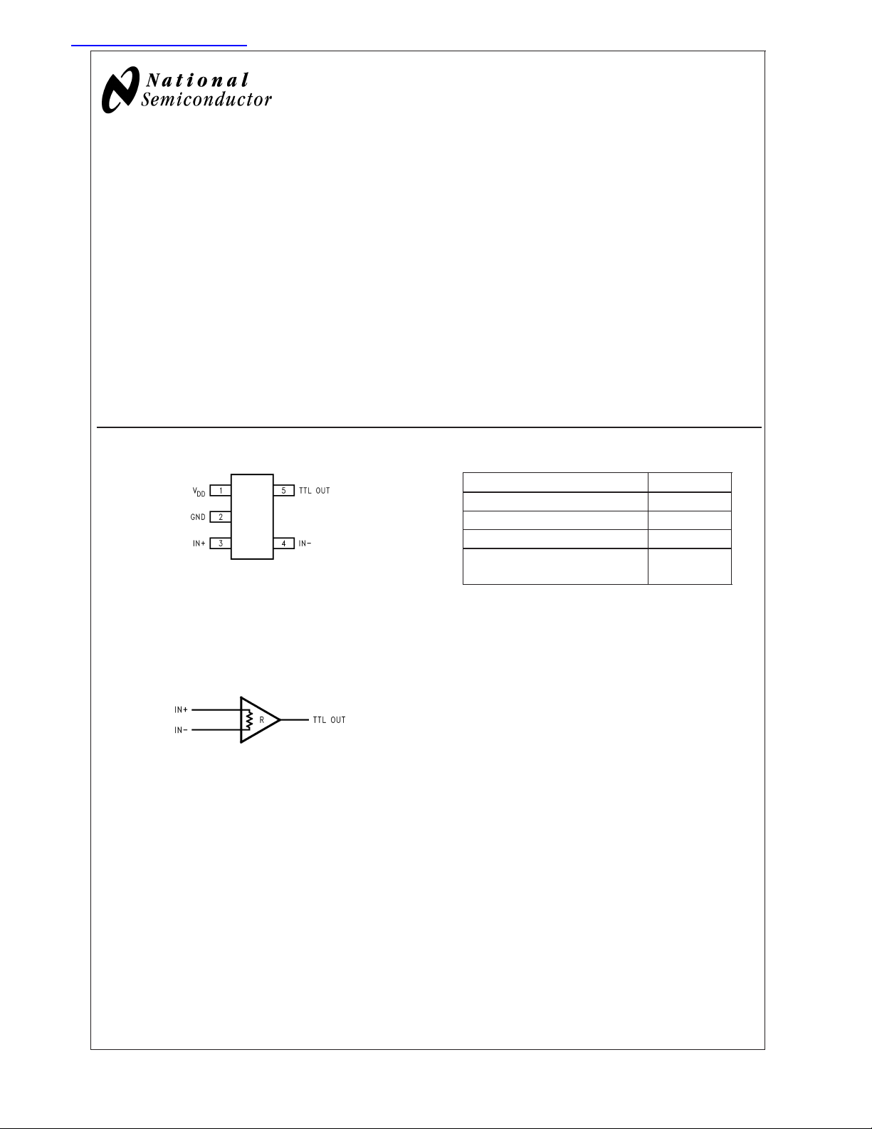
Connection Diagram
20161626
(Top View)
Order Number DS90LT012AHMF
See NS Package Number MF05A
Features
n -40 to +125˚C temperature range operation
n Compatible with ANSI TIA/EIA-644-A Standard
>
n
400 Mbps (200 MHz) switching rates
n 100 ps differential skew (typical)
n 3.5 ns maximum propagation delay
n Integrated line termination resistor (100Ω typical)
n Single 3.3V power supply design (2.7V to 3.6V range)
n Power down high impedance on LVDS inputs
n LVDS inputs accept LVDS/CML/LVPECL signals
n Pinout simplifies PCB layout
n Low Power Dissipation (10mW typical
n SOT-23 5-lead package
@
3.3V static)
Truth Table
INPUTS OUTPUT
[IN+] − [IN−] TTL OUT
V
≥ 0V H
ID
V
≤ −0.1V L
ID
Full Fail-safe OPEN/SHORT or
Terminated
H
Functional Diagram
DS90LT012AH
20161625
© 2005 National Semiconductor Corporation DS201616 www.national.com
Absolute Maximum Ratings (Note 1)
If Military/Aerospace specified devices are required,
please contact the National Semiconductor Sales Office/
Distributors for availability and specifications.
DS90LT012AH
Supply Voltage (V
) −0.3V to +4V
DD
Lead Temperature Range Soldering
(4 sec.) +260˚C
Maximum Junction
Temperature +150˚C
ESD Ratings (Note 4)
Input Voltage (IN+, IN−) −0.3V to +3.9V
Output Voltage (TTL OUT) −0.3V to (V
Output Short Circuit Current −100mA
Maximum Package Power Dissipation
@
+25˚C
MF Package 902mW
Derate MF Package 7.22 mW/˚C above +25˚C
Thermal resistance (θ
) 138.5˚C/W
JA
Storage Temperature Range −65˚C to +150˚C
DD
+ 0.3V)
Recommended Operating
Conditions
Min Typ Max Units
Supply Voltage (V
Operating Free Air
Temperature (T
) +2.7 +3.3 +3.6 V
DD
) −40 25 +125 ˚C
A
Electrical Characteristics
Over Supply Voltage and Operating Temperature ranges, unless otherwise specified. (Notes 2, 3)
Symbol Parameter Conditions Pin Min Typ Max Units
V
TH
V
TL
V
CM
I
IN
∆I
I
IND
R
T
C
IN
V
OH
V
OL
I
OS
V
CL
I
DD
Differential Input High Threshold VCMdependant on VDD(Note 11) IN+, IN− −30 0 mV
Differential Input Low Threshold −100 −30 mV
Common-Mode Voltage VDD= 2.7V, VID= 100mV 0.05 2.35 V
V
= 3.0V to 3.6V, VID= 100mV 0.05 VDD- 0.3V V
DD
T
= 125˚C 0.10 2.35 V
A
Input Current (DS90LV012A) VIN= +2.8V VDD= 3.6V or 0V −10
V
= 0V −10
IN
V
= +3.6V VDD= 0V −20 +20 µA
IN
Change in Magnitude of I
IN
Differential Input Current V
IN
VIN= +2.8V VDD= 3.6V or 0V 4 µA
V
=0V 4 µA
IN
V
= +3.6V VDD=0V 4 µA
IN
IN+
V
IN+
= +0.4V, V
= +2.4V, V
IN−
IN−
= +0V
= +2.0V
±
1 +10 µA
±
1 +10 µA
3 3.9 4.4 mA
Integrated Termination Resistor 100 Ω
Input Capacitance IN+ = IN− = GND 3 pF
Output High Voltage IOH= −0.4 mA, VID= +200 mV TTL OUT 2.4 3.1 V
I
= −0.4 mA, Inputs terminated 2.4 3.1 V
OH
I
= −0.4 mA, Inputs shorted 2.4 3.1 V
OH
Output Low Voltage IOL= 2 mA, VID= −200 mV 0.3 0.5 V
Output Short Circuit Current V
= 0V (Note 5) −15 −50 −100 mA
OUT
Input Clamp Voltage ICL= −18 mA −1.5 −0.7 V
No Load Supply Current Inputs Open V
DD
5.4 9 mA
www.national.com 2
Switching Characteristics
Over Supply Voltage and Operating Temperature ranges, unless otherwise specified. (Notes 6, 7)
Symbol Parameter Conditions Min Typ Max Units
t
PHLD
t
PLHD
t
SKD1
t
SKD3
t
SKD4
t
TLH
t
THL
f
MAX
Differential Propagation Delay High to Low CL= 15 pF 1.0 1.8 3.5 ns
Differential Propagation Delay Low to High VID= 200 mV 1.0 1.7 3.5 ns
Differential Pulse Skew |t
PHLD−tPLHD
| (Note 8) (Figure 1 and Figure 2) 0 100 400 ps
Differential Part to Part Skew (Note 9) 0 0.3 1.0 ns
Differential Part to Part Skew (Note 10) 0 0.4 1.5 ns
Rise Time 350 800 ps
Fall Time 175 800 ps
Maximum Operating Frequency (Note 12) 200 250 MHz
Note 1: “Absolute Maximum Ratings” are those values beyond which the safety of the device cannot be guaranteed. They are not meant to imply that the devices
should be operated at these limits. The table of “Electrical Characteristics” specifies conditions of device operation.
Note 2: Current into device pins is defined as positive. Current out of device pins is defined as negative. All voltages are referenced to ground unless otherwise
specified (such as V
Note 3: All typicals are given for: V
Note 4: ESD Ratings:
DS90LT012AH:
HBM (1.5 kΩ, 100 pF) ≥ 2kV
EIAJ (0Ω, 200 pF) ≥ 700V
CDM ≥ 2000V
IEC direct (330Ω, 150 pF) ≥ 7kV
Note 5: Output short circuit current (I
exceed maximum junction temperature specification.
Note 6: C
Note 7: Generator waveform for all tests unless otherwise specified:f=1MHz, Z
Note 8: t
Note 9: t
and within 5˚C of each other within the operating temperature range.
Note 10: t
recommended operating temperature and voltage ranges, and across process distribution. t
Note 11: V
V
V
Note 12: f
V
over the PVT range by the transition times (t
L
SKD1
SKD3
SKD4
− 0.3V when VDD= 3.0V to 3.6V. VIDis not allowed to be greater than 100 mV when VCM= 0.05V to 2.35V when VDD= 2.7V or when VCM=|VID|/2to
DD
− 0.3V when VDD= 3.0V to 3.6V.
DD
MAX
(max 0.4V), VOH(min 2.4V), load = 15 pF (stray plus probes). The parameter is guaranteed by design. The limit is based on the statistical analysis of the device
OL
).
ID
includes probe and jig capacitance.
is the magnitude difference in differential propagation delay time between the positive-going-edge and the negative-going-edge of the same channel.
, part to part skew, is the differential channel-to-channel skew of any event between devices. This specification applies to devices at the same V
, part to part skew, is the differential channel-to-channel skew of any event between devices. This specification applies to devices over the
is always higher than IN+ and IN− voltage. IN+ and IN− are allowed to have voltage range −0.05V to +2.35V when VDD= 2.7V and |VID|/2to
DD
generator input conditions: tr=t
= +3.3V and TA= +25˚C.
DD
) is specified as magnitude only, minus sign indicates direction only. Only one output should be shorted at a time, do not
OS
=50Ω,trand tf(0% to 100%) ≤ 3 ns for IN±.
O
is defined as |Max − Min| differential propagation delay.
SKD4
<
1 ns (0% to 100%), 50% duty cycle, differential (1.05V to 1.35 peak to peak). Output criteria: 60%/40% duty cycle,
f
and t
THL
).
TLH
DD
DS90LT012AH
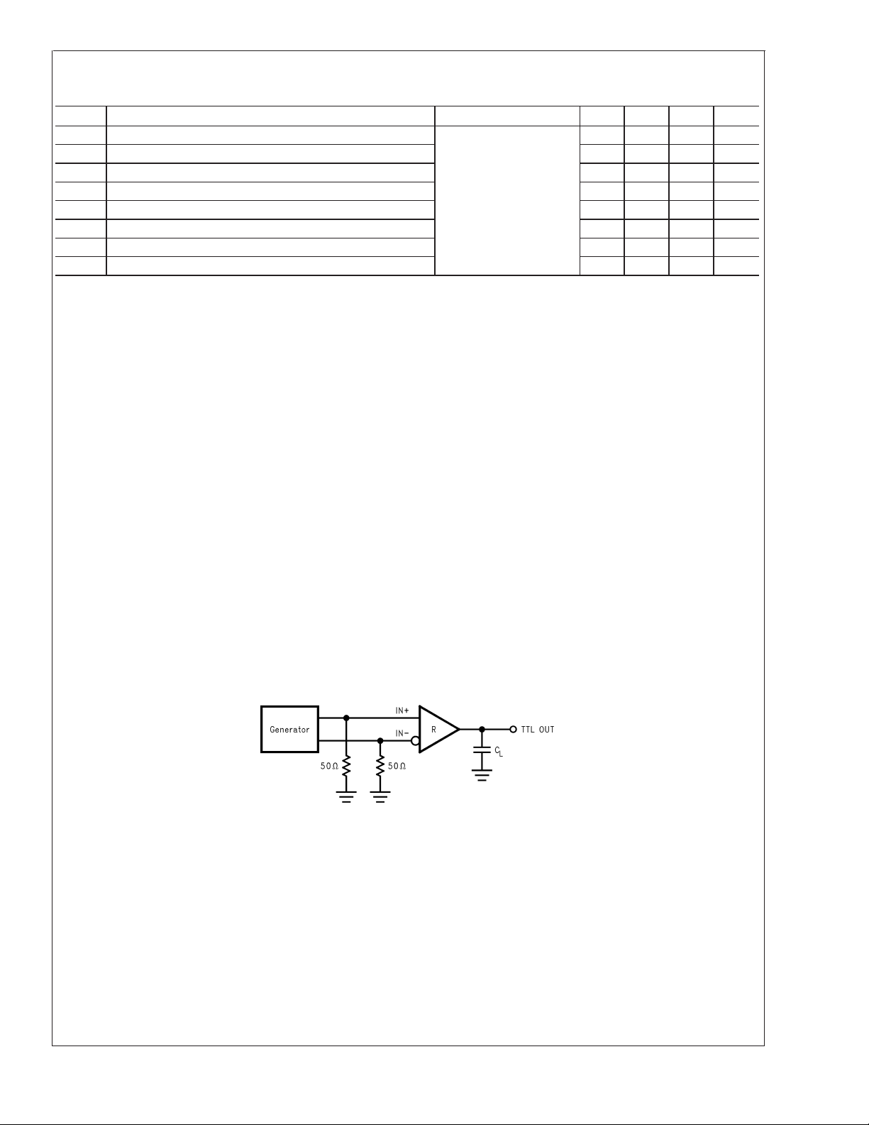
Parameter Measurement Information
FIGURE 1. Receiver Propagation Delay and Transition Time Test Circuit
20161603
www.national.com3
 Loading...