

查询DS90CR211供应商
DS90CR211/DS90CR212
21-Bit Channel Link
General Description
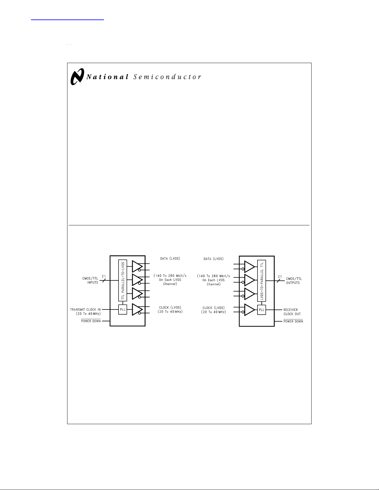
The DS90CR211 transmitter converts 21 bits of CMOS/TTL
data into three LVDS (Low Voltage Differential Signaling)
data streams.Aphase-locked transmit clockis transmitted in
parallel with the data streams over a fourth LVDS link. Every
cycle of the transmit clock 21 bits of input data are sampled
and transmitted. The DS90CR212 receiver converts the
LVDS data streams back into 21 bits of CMOS/TTL data. At
a transmit clock frequency of 40 MHz, 21 bits of TTLdata are
transmitted at a rate of 280 Mbps per LVDS data channel.
Using a 40 MHz clock, the data throughput is 840
Mbit/s(105 Mbyte/s).
The multiplexing of the data lines provides a substantial
cable reduction. Long distance parallel single-ended buses
typically require a ground wire per active signal (and have
very limited noise rejection capability). Thus, for a 21-bit wide
data bus and one clock, up to 44 conductors are required.
With the Channel Link chipset as few as 9 conductors (3
data pairs, 1 clock pair and a minimum of one ground) are
July 1997
needed. This provides a 80%reduction in required cable
width, providing a system cost savings, reduces connector
physical size, and reduces shielding requirements due to the
cables smaller form factor.
The 21 CMOS/TTL inputs can support a variety of signal
combinations. For example, 5 4-bit nibbles plus 1 control, or
2 9-bit (byte + parity) and 3 control.
Features
n Narrow bus reduces cable size and cost
±
n
1V Common mode range (ground shifting)
n 290 mV swing LVDS data transmission
n 840 Mbit/s data throughput
n Low swing differential current mode drivers reduce EMI
n Rising edge data strobe
n Power down mode
n Offered in low profile 48-lead TSSOP package
DS90CR211/DS90CR212 21-Bit Channel Link
Block Diagrams
DS90CR211
Order Number DS90CR211MTD
See NS Package Number MTD48
DS012637-27
DS90CR212
DS012637-1
Order Number DS90CR212MTD
See NS Package Number MTD48
TRI-STATE®is a registered trademark of National Semiconductor Corporation.
© 1998 National Semiconductor Corporation DS012637 www.national.com
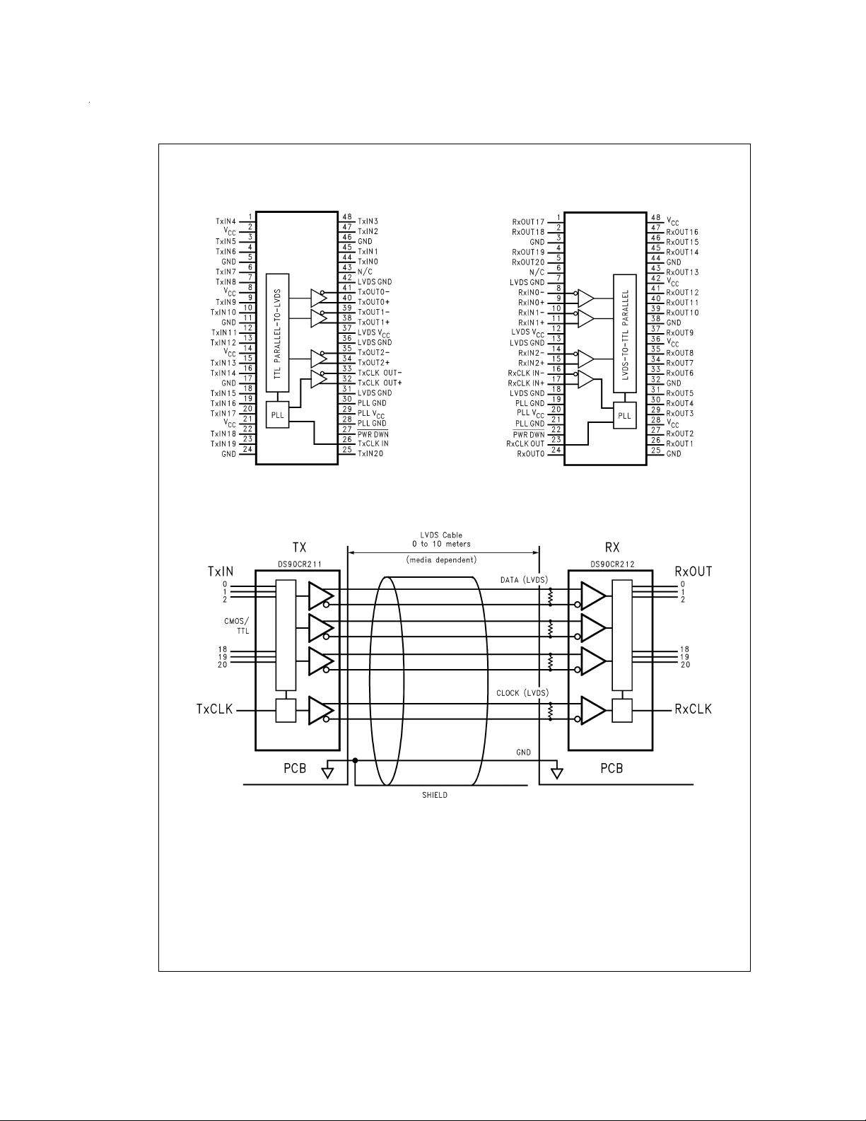
Connection Diagrams
DS90CR211
Typical Application
DS012637-2
DS90CR212
DS012637-3
www.national.com 2
DS012637-19
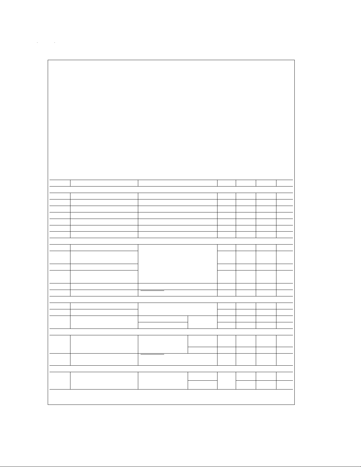
Absolute Maximum Ratings (Note 1)
If Military/Aerospace specified devices are required,
please contact the National Semiconductor Sales Office/
Distributors for availability and specifications.
Supply Voltage (V
CMOS/TTL Input Voltage −0.3V to (V
CMOS/TTL Ouput Voltage −0.3V to (V
LVDS Receiver Input Voltage −0.3V to (V
LVDS Driver Output Voltage −0.3V to (V
LVDS Output
Short Circuit Duration continuous
Junction Temperature +150˚C
Storage Temperature Range −65˚C to +150˚C
Lead Temperature
(Soldering, 4 sec.) +260˚C
Maximum Power Dissipation
) −0.3V to +6V
CC
@
+25˚C
CC
CC
CC
CC
+ 0.3V)
+ 0.3V)
+ 0.3V)
+ 0.3V)
MTD48 (TSSOP) Package:
DS90CR211 1.98W
DS90CR212 1.89W
Package Derating:
DS90CR211 16 mW/˚C above +25˚C
DS90CR212 15 mW/˚C above +25˚C
This device does not meet 2000V ESD rating (Note 4) .
Recommended Operating
Conditions
Supply Voltage (V
) 4.5 5.5 V
CC
Operating Free Air Temperature (T
Receiver Input Range 0 2.4 V
Supply Noise Voltage (V
) 100 mV
CC
Min Max Units
) −10 +70 ˚C
A
Electrical Characteristics
Over recommended operating supply and temperature ranges unless otherwise specified
Symbol Parameter Conditions Min Typ Max Units
CMOS/TTL DC SPECIFICATIONS
V
IH
V
IL
V
OH
V
OL
V
CL
I
IN
I
OS
LVDS DRIVER DC SPEClFlCATIONS
V
OD
∆V
V
CM
∆V
I
OS
I
OZ
LVDS RECEIVER DC SPECIFlCATIONS
V
TH
V
TL
I
IN
TRANSMITTER SUPPLY CURRENT
I
CCTW
I
CCTZ
RECEIVER SUPPLY CURRENT
I
CCRW
High Level Input Voltage 2.0 V
Low Level Input Voltage GND 0.8 V
High Level Output Voltage I
Low Level Output Voltage I
Input Clamp Voltage I
Input Current V
Output Short Circuit Current V
Differential Output Voltage R
Change in VODbetween 35 mV
OD
=
−0.4 mA 3.8 4.9 V
OH
=
2 mA 0.1 0.3 V
OL
=
−18 mA −0.79 −1.5 V
CL
=
, GND, 2.5V or 0.4V
V
IN
CC
=
0V −120 mA
OUT
=
100Ω 250 290 450 mV
L
±
5.1
Complementary Output States
Common Mode Voltage 1.1 1.25 1.375 V
Change in VCMbetween 35 mV
CM
Complementary Output States
Output Short Circuit Current V
OUT
=
Output TRI-STATE®Current Power Down=0V, V
Differential Input High Threshold V
=
CM
=
0V, R
100Ω −2.9 −5 mA
L
OUT
=
0V or V
±
CC
1
+1.2V +100 mV
Differential Input Low Threshold −100 mV
Input Current V
Transmitter Supply Current,
Worst Case
Transmitter Supply Current,
Power Down
Receiver Supply Current,
Worst Case
=
+2.4V V
IN
=
V
0V
IN
=
R
100Ω,C
L
Worst Case Pattern
Figure 1,Figure 2
(
=
L
Power Down=Low
=
C
8 pF,
L
Worst Case Pattern
Figure 1,Figure 3
(
5 pF,
)
)
=
5.5V
CC
<
±
1
<
±
1
f=32.5 MHz 34 51 mA
f=37.5 MHz 36 53 mA
125µA
f=32.5 MHz 55 75 mA
f=37.5 MHz 60 80 mA
CC
±
10 µA
±
10 µA
±
10 µA
±
10 µA
PP
V
www.national.com3
Electrical Characteristics (Continued)
Over recommended operating supply and temperature ranges unless otherwise specified
Symbol Parameter Conditions Min Typ Max Units
RECEIVER SUPPLY CURRENT
I
CCRZ
Note 1: “Absolute Maximum Ratings” are those values beyond which the safety of the device cannot be guaranteed. They are not meant to imply that the device
should be operated at these limits. The tables of “Electrical Characteristics” specify conditions for device operation.
Note 2: Typical values are given for V
Note 3: Current into device pins is defined as positive. Current out of device pins is defined as negative. Voltages are referenced to ground unless otherwise speci-
fied (except V
Note 4: ESD Rating:
Receiver Supply Current,
Power Down
and ∆VOD).
OD
HBM (1.5 kΩ, 100 pF)
PLL V
≥ 1000V
CC
All other pins ≥ 2000V
EIAJ (0Ω, 200 pF) ≥ 150V
CC
=
5.0V and T
Power Down=Low
=
+25˚C.
A
110µA
Transmitter Switching Characteristics
Over recommended operating supply and temperature ranges unless otherwise specified
Symbol Parameter Min Typ Max Units
Figure 2
LLHT LVDS Low-to-High Transition Time (
LHLT LVDS High-to-Low Transition Time (
TCIT TxCLK IN Transition Time (
Figure 4
TCCS TxOUT Channel-to-Channel Skew (Note 5) (
TPPos0 Transmitter Output Pulse Position for Bit0 (
TPPos1 Transmitter Output Pulse Position for Bit1 6.3 7.2 7.5 ns
TPPos2 Transmitter Output Pulse Position for Bit2 12.8 13.6 14.6 ns
TPPos3 Transmitter Output Pulse Position for Bit3 20 20.8 21.5 ns
TPPos4 Transmitter Output Pulse Position for Bit4 27.2 28 28.5 ns
TPPos5 Transmitter Output Pulse Position for Bit5 34.5 35.2 35.6 ns
TPPos6 Transmitter Output Pulse Position for Bit6 42.2 42.6 42.9 ns
TPPos0 Transmitter Output Pulse Position for Bit0 (
TPPos1 Transmitter Output Pulse Position for Bit1 2.9 3.3 3.9 ns
TPPos2 Transmitter Output Pulse Position for Bit2 6.1 6.6 7.1 ns
TPPos3 Transmitter Output Pulse Position for Bit3 9.7 10.2 10.7 ns
TPPos4 Transmitter Output Pulse Position for Bit4 13 13.5 14.1 ns
TPPos5 Transmitter Output Pulse Position for Bit5 17 17.4 17.8 ns
TPPos6 Transmitter Output Pulse Position for Bit6 20.3 20.8 21.4 ns
TCIP TxCLK IN Period (
TCIH TxCLK IN High Time (
TCIL TxCLK IN Low Time (
TSTC TxIN Setup to TxCLK IN (
THTC TxIN Hold to TxCLK IN (
TCCD TxCLK IN to TxCLK OUT Delay
Figure 6
) 25 T 50 ns
Figure 6
) 0.35T 0.5T 0.65T ns
Figure 6
) 0.35T 0.5T 0.65T ns
Figure 6
) f = 20 MHz 14 ns
Figure 6
) 2.5 2 ns
@
TPLLS Transmitter Phase Lock Loop Set (
TPDD Transmitter Powerdown Delay (
Note 5: This limit based on bench characterization.
Figure 14
) 0.75 1.5 ns
Figure 2
) 0.75 1.5 ns
)8ns
Figure 5
) 350 ps
Figure 16
Figure 16
)f
)f
=
20 MHz −200 150 350 ps
=
40 MHz −100 100 300 ps
f=40MHz 8 ns
25˚C, V
Figure 10
=
Figure 8
5.0V (
CC
) 5 9.7 ns
)10ms
) 100 ns
www.national.com 4
Receiver Switching Characteristics
Over recommended operating supply and temperature ranges unless otherwise specified
Symbol Parameter Min Typ Max Units
Figure 3
CLHT CMOS/TTL Low-to-High Transition Time (
CHLT CMOS/TTL High-to-Low Transition Time (
RCOP RxCLK OUT Period (
Figure 7
) 25 T 50 ns
) 3.5 6.5 ns
Figure 3
) 2.7 6.5 ns
RSKM Receiver Skew Margin (Note 6) f=20 MHz 1.1 ns
=
V
CC
5V, T
=
25˚C (
A
RCOH RxCLK OUT High Time (
Figure 17
)f
Figure 7
)f
=
40 MHz 700 ps
=
20 MHz 19 ns
f=40 MHz 6 ns
RCOL RxCLK OUT Low Time (
Figure 7
)f
=
20 MHz 21.5 ns
f=40 MHz 10.5 ns
RSRC RxCLK Setup to RxCLK OUT (
Figure 7
)f
=
20 MHz 14 ns
f=40 MHz 4.5 ns
RHRC RxCLK Hold to RxCLK OUT (
Figure 7
)f
=
20 MHz 16 ns
f=40 MHz 6.5 ns
RCCD RxCLK IN to RxCLK OUT Delay
RPLLS Receiver Phase Lock Loop Set (
RPDD Receiver Powerdown Delay (
Note 6: Receiver Skew Margin is defined as the valid data sampling region at the receiver inputs. This margin takes into account for transmitter output skew(TCCS)
and the setup and hold time (internal data sampling window), allowing LVDS cable skew dependent on type/length and source clock(TxCLK IN) jitter.
RSKM ≥ cable skew (type, length) + source clock jitter (cycle to cycle).
@
25˚C, V
Figure 11
Figure 15
=
Figure 9
5.0V (
CC
) 7.6 11.9 ns
)10ms
)1µs
AC Timing Diagrams
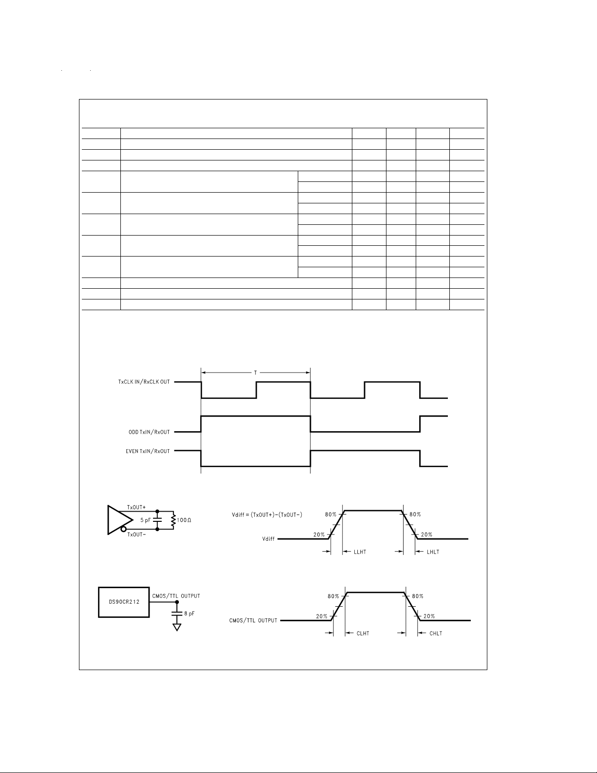
FIGURE 1. “WORST CASE” Test Pattern
DS012637-5
FIGURE 2. DS90CR211 (Transmitter) LVDS Output Load and Transition Timing
DS012637-7
FIGURE 3. DS90CR212 (Receiver) CMOS/TTL Output Load and Transition Timing
DS012637-4
DS012637-6
DS012637-8
www.national.com5
 Loading...