

查询DS90CP22供应商
DS90CP22
2X2 800 Mbps LVDS Crosspoint Switch
2X2 800 Mbps LVDS Crosspoint Switch
November 2003
General Description
DS90CP22 is a 2x2 crosspoint switch utilizing LVDS (Low
Voltage Differential Signaling) technology for low power, high
speed operation. Data paths are fully differential from input
to output for low noise generation and low pulse width distortion. The non-blocking design allows connection of any
input to any output or outputs. LVDS I/O enable high speed
data transmission for point-to-point interconnects. This device can be used as a high speed differential crosspoint, 2:1
mux, 1:2 demux, repeater or 1:2 signal splitter. The mux and
demux functions are useful for switching between primary
and backup circuits in fault tolerant systems. The 1:2 signal
splitter and 2:1 mux functions are useful for distribution of
serial bus across several rack-mounted backplanes.
The DS90CP22 accepts LVDS signal levels, LVPECL levels
directly or PECL with attenuation networks.
The individual LVDS outputs can be put into TRI-STATE by
use of the enable pins.
For more details, please refer to the Application Information
section of this datasheet.
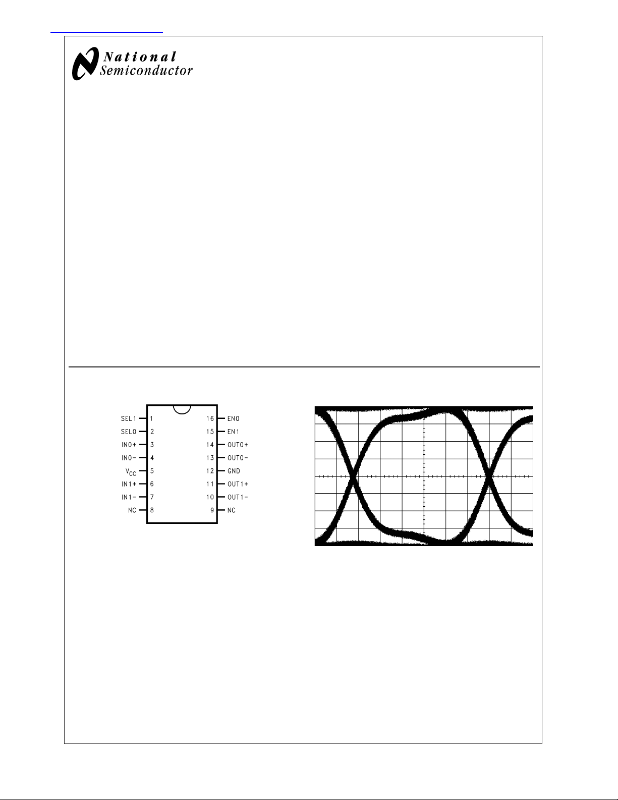
Connection Diagrams
Features
n Low jitter 800 Mbps fully differential data path
n 75 ps (typ) of pk-pk jitter with PRBS = 2
pattern at 800 Mbps
n Single +3.3 V Supply
n Less than 330 mW (typ) total power dissipation
n Non-blocking "’Switch Architecture"’
n Balanced output impedance
n Output channel-to-channel skew is 35 ps (typ)
n Configurable as 2:1 mux, 1:2 demux, repeater or 1:2
signal splitter
n LVDS receiver inputs accept LVPECL signals
n Fast switch time of 1.2ns (typ)
n Fast propagation delay of 1.3ns (typ)
<
n Receiver input threshold
n Available in 16 lead TSSOP and SOIC packages
n Inter-operates with ANSI/TIA/EIA-644-1995 LVDS
standard
n Operating Temperature: −40˚C to +85˚C
±
100 mV
23
−1 data
Order Number DS90CP22M-8 (SOIC)
Order Number DS90CP22MT (TSSOP)
© 2003 National Semiconductor Corporation DS101053 www.national.com
10105305
Diff. Output Eye-Pattern in 1:2 split mode@800 Mbps
Conditions: 3.3 V, PRBS = 2
= 300mV, VCM= +1.2 V, 200 ps/div, 100 mV/div
V
ID
23
−1 data pattern,
10105310
Absolute Maximum Ratings (Note 1)
If Military/Aerospace specified devices are required,
please contact the National Semiconductor Sales Office/
DS90CP22
Distributors for availability and specifications.
Supply Voltage (V
CMOS/TTL Input Voltage (EN0,
EN1, SEL0, SEL1)
LVDS Receiver Input Voltage
) −0.3V to +4V
CC
−0.3V to (V
CC
+ 0.3V)
Maximum Package Power Dissipation at 25˚C
16L SOIC 1.435 W
16L SOIC Package Derating 11.48 mW/˚C above +25˚C
16L TSSOP 0.866 W
16L TSSOP Package Derating 9.6 mW/˚C above +25˚C
ESD Rating:
(HBM, 1.5kΩ, 100pF)
(EIAJ, 0Ω, 200pF)
(IN+, IN−) −0.3V to +4V
LVDS Driver Output Voltage
(OUT+, OUT−) −0.3V to +4V
LVDS Output Short Circuit
Current
Continuous
Junction Temperature +150˚C
Storage Temperature Range −65˚C to +150˚C
Lead Temperature
Recommended Operating
Conditions
Min Typ Max Units
Supply Voltage (V
Receiver Input Voltage 0 V
Operating Free Air Temperature -40 +25 +85 ˚C
) 3.0 3.3 3.6 V
CC
(Soldering, 4 sec.) +260˚C
Electrical Characteristics
Over recommended operating supply and temperature ranges unless otherwise specified
Symbol Parameter Conditions Min Typ Max Units
CMOS/TTL DC SPECIFICATIONS (EN0,EN1,SEL0,SEL1)
V
IH
V
IL
I
IH
I
IL
V
CL
LVDS OUTPUT DC SPECIFICATIONS (OUT0,OUT1)
V
OD
∆V
OD
V
OS
∆V
OS
I
OZ
I
OFF
I
OS
I
OSB
LVDS RECEIVER DC SPECIFICATIONS (IN0,IN1)
V
TH
V
TL
V
CMR
I
IN
SUPPLY CURRENT
I
CCD
I
CCZ
Note 1: “Absolute Maximum Ratings” are these beyond which the safety of the device cannot be guaranteed. They are not meant to imply that the device should
be operated at these limits. The table of “Electrical Characteristics” provides conditions for actual device operation.
Note 2: All typical are given for V
Note 3: V
High Level Input Voltage 2.0 V
Low Level Input Voltage GND 0.8 V
High Level Input Current VIN= 3.6V or 2.0V; VCC= 3.6V +7 +20 µA
Low Level Input Current VIN= 0V or 0.8V; VCC= 3.6V
±
±
1
Input Clamp Voltage ICL= −18 mA −0.8 −1.5 V
Differential Output Voltage RL=75Ω 270 365 475 mV
R
=75Ω,VCC= 3.3V, TA= 25˚C 285 365 440 mV
L
Change in VODbetween Complimentary Output States 35 mV
Offset Voltage (Note 3) 1.0 1.2 1.45 V
Change in VOSbetween Complimentary Output States 35 mV
Output TRI-STATE®Current TRI-STATE Output,
V
OUT=VCC
Power-Off Leakage Current VCC= 0V; V
Output Short Circuit Current V
Both Outputs Short Circuit Current V
OUT+
OUT+
OR V
AND V
or GND
= 3.6V or GND
OUT
OUT−
OUT−
±
±
= 0V −15 −25 mA
= 0V −30 −50 mA
±
1
±
1
Differential Input High Threshold VCM= +0.05V or +1.2V or +3.25V, 0 +100 mV
Differential Input Low Threshold Vcc = 3.3V −100 0 mV
Common Mode Voltage Range VID= 100mV, Vcc = 3.3V 0.05 3.25 V
Input Current VIN= +3.0V, VCC= 3.6V or 0V
V
= 0V, VCC= 3.6V or 0V
IN
Total Supply Current RL=75Ω,CL= 5 pF,
±
±
98 125 mA
±
1
±
1
EN0 = EN1 = High
TRI-STATE Supply Current EN0 = EN1 = Low 43 55 mA
= +3.3V and TA= +25˚C, unless otherwise stated.
is defined and measured on the ATE as (VOH+VOL)/2.
OS
CC
>
>
250 V
CC
CC
10 µA
10 µA
10 µA
10 µA
10 µA
5kV
V
V
www.national.com 2
AC Electrical Characteristics
Over recommended operating supply and temperature ranges unless otherwise specified (Note 4)
Symbol Parameter Conditions Min Typ Max Units
T
SET
T
HOLD
T
SWITCH
T
PHZ
T
PLZ
T
PZH
T
PZL
T
LHT
T
HLT
T
JIT
T
PLHD
T
PHLD
T
SKEW
T
CCS
Note 4: The parameters are guaranteed by design. The limits are based on statistical analysis of the device performance over PVT (process, voltage and
temperature) range.
Note 5: T
Note 6: The parameters are guaranteed by design. The limits are based on statistical analysis of the device performance over PVT range with the following
equipment test setup: HP70004A (display mainframe) with HP70841B (pattern generator), 5 feet of RG-142 cable with DUT test board and HP83480A(digital scope
mainframe) with HP83483A (20GHz scope module).
Input to SEL Setup Time, Figures 1, 2
0.7 0.5 ns
(Note 5)
Input to SEL Hold Time, Figures 1, 2
1.0 0.5 ns
(Note 5)
SEL to Switched Output, Figures 1, 2 0.9 1.2 1.7 ns
Disable Time (Active to TRI-STATE) High to Z, Figure 3 2.1 4.0 ns
Disable Time (Active to TRI-STATE) Low to Z, Figure 3 3.0 4.5 ns
Enable Time (TRI-STATE to Active) Z to High, Figure 3 25.5 55.0 ns
Enable Time (TRI-STATE to Active) Z to Low, Figure 3 25.5 55.0 ns
Output Low-to-High Transition Time, 20% to 80%, Figure 5 290 400 580 ps
Output High-to-Low Transition Time, 80% to 20%, Figure 5 290 400 580 ps
LVDS Data Path Peak to Peak Jitter,
(Note 6)
VID= 300mV; 50% Duty Cycle;
= 1.2V at 800Mbps
V
CM
V
= 300mV; PRBS=223-1 data
ID
pattern; V
= 1.2V at 800Mbps
CM
40 90 ps
75 190 ps
Propagation Low to High Delay, Figure 6 0.9 1.3 1.6 ns
Propagation Low to High Delay, Figure 6 V
= 3.3V, TA= 25˚C 1.0 1.3 1.5 ns
CC
Propagation High to Low Delay, Figure 6 0.9 1.3 1.6 ns
Propagation High to Low Delay, Figure 6 V
Pulse Skew |T
PLHD-TPHLD
| 0 225 ps
= 3.3V, TA= 25˚C 1.0 1.3 1.5 ns
CC
Output Channel-to-Channel Skew, Figure 7 35 80 ps
SET
and T
time specify that data must be in a stable state before and after the SEL transition.
HOLD
DS90CP22
www.national.com3
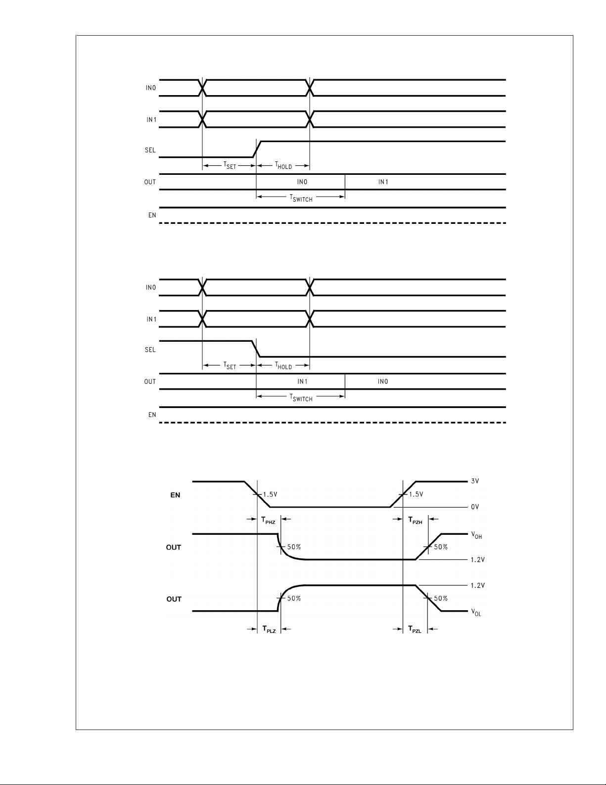
AC Timing Diagrams
DS90CP22
FIGURE 1. Input-to-Select rising edge setup and hold times and mux switch time
10105302
FIGURE 2. Input-to-Select falling edge setup and hold times and mux switch time
10105304
FIGURE 3. Output active to TRI-STATE and TRI-STATE to active output time
10105303
www.national.com 4

AC Timing Diagrams (Continued)
FIGURE 5. LVDS Output Transition Time
DS90CP22
10105306
FIGURE 4. LVDS Output Load
10105309
10105307
FIGURE 6. Propagation Delay Low-to-High and High-to-Low
10105308
FIGURE 7. Output Channel-to-Channel Skew in 1:2 splitter mode
www.national.com5

DS90CP22 Pin Description
Pin Name # of Pin Input/Output Description
DS90CP22
IN+ 2 I Non-inverting LVDS input
IN - 2 I Inverting LVDS input
OUT+ 2 O Non-inverting LVDS Output
OUT - 2 O Inverting LVDS Output
EN 2 I A logic low on the Enable puts the LVDS output into
SEL 2 I 2:1 mux input select
GND 1 P Ground
V
CC
NC 2 No Connect
TRI-STATE and reduces the supply current
1 P Power Supply
Application Information
MODES OF OPERATION
The DS90CP22 provides three modes of operation. In the
1:2 splitter mode, the two outputs are copies of the same
single input. This is useful for distribution / fan-out applications. In the repeater mode, the device operates as a 2
channel LVDS buffer. Repeating the signal restores the
LVDS amplitude, allowing it to drive another media segment.
This allows for isolation of segments or long distance applications. The switch mode provides a crosspoint function.
This can be used in a system when primary and redundant
paths are supported in fault tolerant applications.
INPUT FAIL-SAFE
The receiver inputs of the DS90CP22 do not have internal
fail-safe biasing. For point-to-point and multidrop applications with a single source, fail-safe biasing may not be
required. When the driver is off, the link is in-active. If failsafe biasing is required, this can be accomplished with external high value resistors. The IN+ should be pull to Vcc with
10kΩ and the IN− should be pull to Gnd with 10kΩ. This
provides a slight positive differential bias, and sets a known
HIGH state on the link with a minimum amount of distortion.
UNUSED LVDS INPUTS
Unused LVDS Receiver inputs should be tied off to prevent
the high-speed sensitive input stage from picking up noise
signals. The open input to IN+ should be pull to Vcc with
10kΩ and the open input to IN− should be pull to Gnd with
10kΩ.
UNUSED CONTROL INPUTS
The SEL and EN control input pins have internal pull down
devices. Unused pins may be tied off or left as no-connect (if
a LOW state is desired).
EXPANDING THE NUMBER OF OUTPUT PORTS
To expand the number of output ports, more than one
DS90CP22 can be used. Total propagation delay through the
devices should be considered to determine the maximum
expansion. For example, if2X4isdesired, than three of the
DS90CP22 are required. A minimum of two device propagation delays (2 x 1.3ns = 2.6ns (typ)) can be achieved. For a
2 X 8, a total of 7 devices must be used with propagation
delay of 3 x 1.3ns = 3.9ns (typ). The power consumption will
increase proportional to the number of devices used.
PCB LAYOUT AND POWER SYSTEM BYPASS
Circuit board layout and stack-up for the DS90CP22 should
be designed to provide noise-free power to the device. Good
layout practice also will separate high frequency or high level
inputs and outputs to minimize unwanted stray noise pickup,
feedback and interference. Power system performance may
be greatly improved by using thin dielectrics (4 to 10 mils) for
power/ground sandwiches. This increases the intrinsic capacitance of the PCB power system which improves power
supply filtering, especially at high frequencies, and makes
the value and placement of external bypass capacitors less
critical. External bypass capacitors should include both RF
ceramic and tantalum electrolytic types. RF capacitors may
use values in the range 0.01 µF to 0.1 µF. It is recommended
practice to use two vias at each power pin of the DS90CP22
as well as all RF bypass capacitor terminals. Dual vias
reduce the interconnect inductance by up to half, thereby
reducing interconnect inductance and extending the effective frequency range of the bypass components.
The outer layers of the PCB may be flooded with additional
ground plane. These planes will improve shielding and isolation as well as increase the intrinsic capacitance of the
power supply plane system. Naturally, to be effective, these
planes must be tied to the ground supply plane at frequent
intervals with vias. Frequent via placement also improves
signal integrity on signal transmission lines by providing
short paths for image currents which reduces signal distortion.
There are more common practices which should be followed
when designing PCBs for LVDS signaling. Please see Application Note: AN-1108 for additional information.
COMPATIBILITY WITH LVDS STANDARD
The DS90CP22 is compatible with LVDS and Bus LVDS
Interface devices. It is enhanced over standard LVDS drivers
in that it is able to driver lower impedance loads with standard LVDS levels. Standard LVDS drivers provide 330mV
differential output with a 100Ω load. The DS90CP22 provides 365mV with a 75Ω load or 400mV with 100Ω loads.
This extra drive capability is useful in certain multidrop applications.
In backplane multidrop configurations, with closely spaced
loads, the effective differential impedance of the line is reduced. If the mainline has been designed for 100Ω differential impedance, the loading effects may reduce this to the
70Ω range depending upon spacing and capacitance load.
Terminating the line with a 75Ω load is a better match than
with 100Ω and reflections are reduced.
www.national.com 6
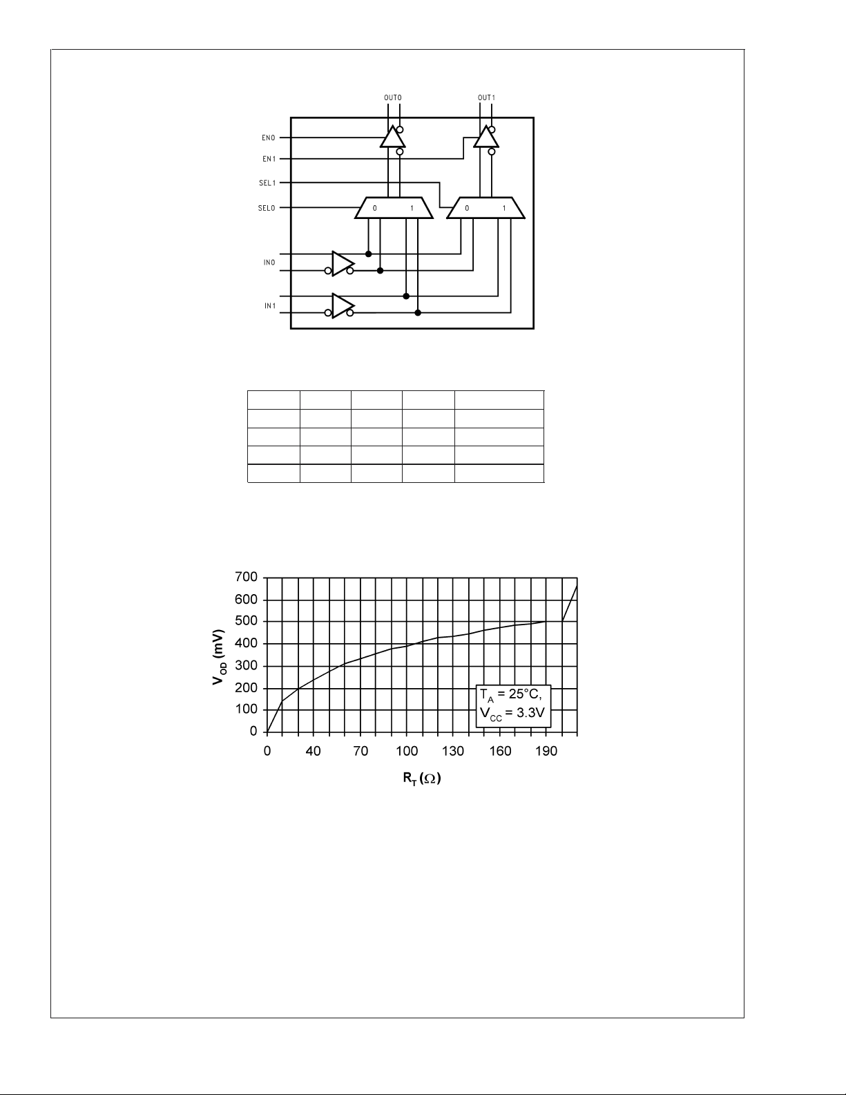
Block Diagram
DS90CP22
10105301
Function Table
SEL0 SEL1 OUT0 OUT1 Mode
0 0 IN0 IN0 1:2 splitter
0 1 IN0 IN1 repeater
1 0 IN1 IN0 switch
1 1 IN1 IN1 1:2 splitter
Note: 0 = low, 1 = high
EN0 = EN1 = 1 for enable
Typical Performance Characteristics
Diff. Output Voltage (VOD) vs. Resistive Load (RT)
10105311
www.national.com7

Typical Performance Characteristics (Continued)
DS90CP22
Peak-to-Peak Output Jitter at V
= +0.4V vs. VID
CM
10105312
Peak-to-Peak Output Jitter at VCM= +1.2V vs. VID
Peak-to-Peak Output Jitter at VCM= +1.6V vs. VID
www.national.com 8
10105313
10105314

Physical Dimensions inches (millimeters)
unless otherwise noted
DS90CP22
Order Number DS90CP22M-8
See NS Package Number M16A
16-Lead (4.4mm Wide) Molded Thin Shrink Small Outline Package, JEDEC
Order Number DS90CP22MT
Order Number DS90CP22MTX (Tape and Reel)
See NS Package Number MTC16
www.national.com9

2X2 800 Mbps LVDS Crosspoint Switch
Notes
LIFE SUPPORT POLICY
NATIONAL’S PRODUCTS ARE NOT AUTHORIZED FOR USE AS CRITICAL COMPONENTS IN LIFE SUPPORT
DEVICES OR SYSTEMS WITHOUT THE EXPRESS WRITTEN APPROVAL OF THE PRESIDENT AND GENERAL
COUNSEL OF NATIONAL SEMICONDUCTOR CORPORATION. As used herein:
1. Life support devices or systems are devices or
systems which, (a) are intended for surgical implant
into the body, or (b) support or sustain life, and
whose failure to perform when properly used in
accordance with instructions for use provided in the
2. A critical component is any component of a life
support device or system whose failure to perform
can be reasonably expected to cause the failure of
the life support device or system, or to affect its
safety or effectiveness.
labeling, can be reasonably expected to result in a
significant injury to the user.
BANNED SUBSTANCE COMPLIANCE
National Semiconductor certifies that the products and packing materials meet the provisions of the Customer Products
Stewardship Specification (CSP-9-111C2) and the Banned Substances and Materials of Interest Specification
(CSP-9-111S2) and contain no ‘‘Banned Substances’’ as defined in CSP-9-111S2.
National Semiconductor
Americas Customer
Support Center
Email: new.feedback@nsc.com
Tel: 1-800-272-9959
www.national.com
National does not assume any responsibility for use of any circuitry described, no circuit patent licenses are implied and National reserves the right at any time without notice to change said circuitry and specifications.
National Semiconductor
Europe Customer Support Center
Fax: +49 (0) 180-530 85 86
Email: europe.support@nsc.com
Deutsch Tel: +49 (0) 69 9508 6208
English Tel: +44 (0) 870 24 0 2171
Français Tel: +33 (0) 1 41 91 8790
National Semiconductor
Asia Pacific Customer
Support Center
Email: ap.support@nsc.com
National Semiconductor
Japan Customer Support Center
Fax: 81-3-5639-7507
Email: jpn.feedback@nsc.com
Tel: 81-3-5639-7560
 Loading...