

查询DS90CF366供应商
DS90CF386/DS90CF366
+3.3V LVDS Receiver 24-Bit Flat Panel Display (FPD)
Link—85 MHz, +3.3V LVDS Receiver 18-Bit Flat Panel
Display (FPD) Link—85 MHz
General Description
The DS90CF386 receiver converts the four LVDS data
streams (Up to 2.38 Gbps throughput or 297.5 Megabytes/
sec bandwidth) back into parallel 28 bits of CMOS/TTL data
(24 bits of RGB and 4 bits of Hsync, Vsync, DE and CNTL).
Also available is the DS90CF366 that converts the three
LVDS data streams (Up to 1.78 Gbps throughput or 223
Megabytes/sec bandwidth) back into parallel 21 bits of
CMOS/TTL data (18 bits of RGB and 3 bits of Hsync, Vsync
and DE). Both Receivers’ outputs are Falling edge strobe. A
Rising edge or Falling edge strobe transmitter (DS90C385/
DS90C365) will interoperate with a Falling edge strobe Receiver without any translation logic.
The DS90CF386 is also offered in a 64 ball, 0.8mm fine pitch
ball grid array (FBGA) package which provides a 44 %
reduction in PCB footprint compared to the 56L TSSOP
package.
This chipset is an ideal means to solve EMI and cable size
problems associated with wide, high speed TTL interfaces.
Features
n 20 to 85 MHz shift clock support
n Rx power consumption
Grayscale
n Rx Power-down mode
n ESD rating
n Supports VGA, SVGA, XGA and Single Pixel SXGA.
n PLL requires no external components
n Compatible with TIA/EIA-644 LVDS standard
n Low profile 56-lead or 48-lead TSSOP package
n DS90CF386 also available in a 64 ball, 0.8mm fine pitch
ball grid array (FBGA) package
>
7 kV (HBM),>700V (EIAJ)
<
142 mW (typ)@85MHz
<
1.44 mW (max)
May 2003
DS90CF386/DS90CF366 +3.3V LVDS Receiver 24-Bit-Color Flat Panel Display (FPD)
Link—85 MHz, +3.3V LVDS Receiver 18-Bit-Color Flat Panel Display (FPD) Link—85 MHz
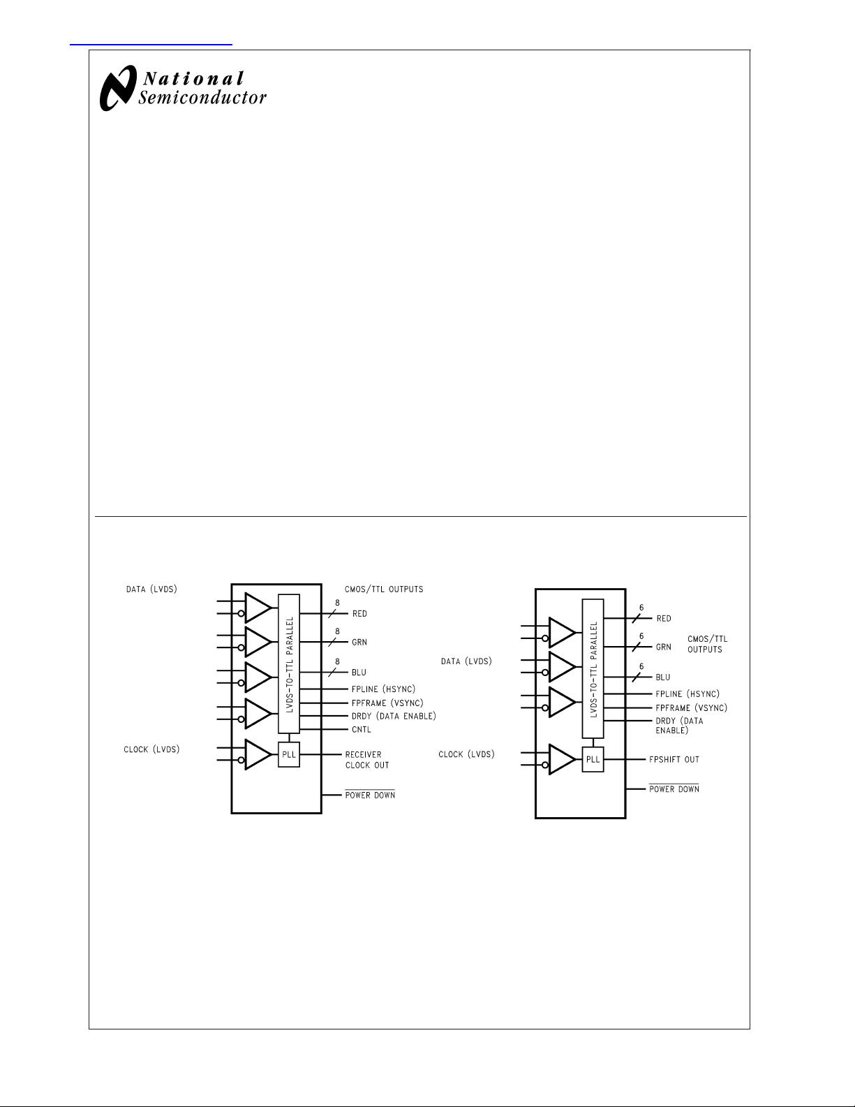
Block Diagrams
DS90CF386 DS90CF366
Order Number DS90CF386MTD or DS90CF386SLC
See NS Package Number MTD56 or SLC64A
10108527
Order Number DS90CF366MTD
10108528
See NS Package Number MTD48
TRI-STATE®is a registered trademark of National Semiconductor Corporation.
© 2003 National Semiconductor Corporation DS101085 www.national.com
Absolute Maximum Ratings (Note 1)
If Military/Aerospace specified devices are required,
please contact the National Semiconductor Sales Office/
Distributors for availability and specifications.
Supply Voltage (V
CMOS/TTL Output Voltage −0.3V to (V
LVDS Receiver Input Voltage −0.3V to (V
Junction Temperature +150˚C
DS90CF386/DS90CF366
Storage Temperature −65˚C to +150˚C
Lead Temperature
(Soldering, 4 sec for TSSOP) +260˚C
) −0.3V to +4V
CC
CC
CC
+ 0.3V)
+ 0.3V)
DS90CF366MTD 15 mW/˚C above +25˚C
Maximum Package Power
Dissipation Capacity
@
25˚C
SLC64A Package:
DS90CF386SLC 2.0 W
Package Derating:
DS90CF386SLC 10.2 mW/˚C above +25˚C
ESD Rating
(HBM, 1.5 kΩ, 100 pF)
(EIAJ, 0Ω, 200 pF)
Solder Reflow Temperature
(Soldering, 20 sec for FBGA) +220˚C
Maximum Package Power
Dissipation Capacity
@
25˚C
MTD56 (TSSOP) Package:
DS90CF386MTD 1.61 W
MTD48 (TSSOP) Package:
DS90CF366MTD 1.89 W
Package Derating:
DS90CF386MTD 12.4 mW/˚C above +25˚C
Recommended Operating
Conditions
Min Nom Max Units
Supply Voltage (V
Operating Free Air
Temperature (T
Receiver Input Range 0 2.4 V
Supply Noise Voltage (V
) 3.0 3.3 3.6 V
CC
) −10 +25 +70 ˚C
A
) 100 mV
CC
Electrical Characteristics
Over recommended operating supply and temperature ranges unless otherwise specified.
Symbol Parameter Conditions Min Typ Max Units
CMOS/TTL DC SPECIFICATIONS
V
IH
V
IL
V
OH
V
OL
V
CL
I
IN
I
OS
LVDS RECEIVER DC SPECIFICATIONS
V
TH
V
TL
I
IN
RECEIVER SUPPLY CURRENT
ICCRW Receiver Supply Current C
High Level Input Voltage 2.0 VCC V
Low Level Input Voltage GND 0.8 V
High Level Output Voltage IOH= - 0.4 mA 2.7 3.3 V
Low Level Output Voltage IOL= 2 mA 0.06 0.3 V
Input Clamp Voltage ICL= −18 mA -0.79 -1.5 V
Input Current VIN= 0.4V, 2.5V or V
V
= GND -10 0 uA
IN
Output Short Circuit Current V
= 0V -60 -120 mA
OUT
CC
+1.8 +15 uA
Differential Input High Threshold VCM= +1.2V +100 mV
Differential Input Low Threshold −100 mV
Input Current VIN= +2.4V, VCC= 3.6V
V
= 0V, VCC= 3.6V
IN
= 8 pF, f = 32.5 MHz 49 70 mA
L
±
10 µA
±
10 µA
Worst Case Worst Case Pattern, f = 37.5 MHz 53 75 mA
DS90CF386 (Figures 1,4)f = 65 MHz 81 114 mA
>
>
7kV
700V
PP
ICCRW Receiver Supply Current C
= 8 pF, f = 32.5 MHz 49 60 mA
L
Worst Case Worst Case Pattern, f = 37.5 MHz 53 65 mA
DS90CF366 (Figures 1,4)f = 65 MHz 78 100 mA
ICCRG Receiver Supply Current, C
= 8 pF, f = 32.5 MHz 28 45 mA
L
16 Grayscale 16 Grayscale Pattern, f = 37.5 MHz 30 47 mA
www.national.com 2
f = 85 MHz 96 135 mA
f = 85 MHz 90 115 mA
DS90CF386/DS90CF366
Electrical Characteristics (Continued)
Over recommended operating supply and temperature ranges unless otherwise specified.
Symbol Parameter Conditions Min Typ Max Units
RECEIVER SUPPLY CURRENT
(Figures 2, 3, 4 ) f = 65 MHz 43 60 mA
f = 85 MHz 43 70 mA
ICCRZ Receiver Supply Current Power Down = Low
140 400 µA
Power Down Receiver Outputs Stay Low during
Power Down Mode
Note 1: “Absolute Maximum Ratings” are those values beyond which the safety of the device cannot be guaranteed. They are not meant to imply that the device
should be operated at these limits. The tables of “Electrical Characteristics” specify conditions for device operation.
Note 2: Typical values are given for V
Note 3: Current into device pins is defined as positive. Current out of device pins is defined as negative. Voltages are referenced to ground unless otherwise
specified (except V
and ∆VOD).
OD
= 3.3V and TA= +25C.
CC
Receiver Switching Characteristics
Over recommended operating supply and temperature ranges unless otherwise specified
Symbol Parameter Min Typ Max Units
CLHT CMOS/TTL Low-to-High Transition Time (Figure 4 ) 2.0 3.5 ns
CHLT CMOS/TTL High-to-Low Transition Time (Figure 4 ) 1.8 3.5 ns
RSPos0 Receiver Input Strobe Position for Bit 0 (Figure 11,
Figure 12 )
RSPos1 Receiver Input Strobe Position for Bit 1 2.17 2.52 2.87 ns
RSPos2 Receiver Input Strobe Position for Bit 2 3.85 4.20 4.55 ns
RSPos3 Receiver Input Strobe Position for Bit 3 5.53 5.88 6.23 ns
RSPos4 Receiver Input Strobe Position for Bit 4 7.21 7.56 7.91 ns
RSPos5 Receiver Input Strobe Position for Bit 5 8.89 9.24 9.59 ns
RSPos6 Receiver Input Strobe Position for Bit 6 10.57 10.92 11.27 ns
RSKM RxIN Skew Margin (Note 4) (Figure 13 ) f = 85 MHz 290 ps
RCOP RxCLK OUT Period (Figure 5) 11.76 T 50 ns
RCOH RxCLK OUT High Time (Figure 5 ) f = 85 MHz 4.5 5 7 ns
RCOL RxCLK OUT Low Time (Figure 5) 4.0 5 6.5 ns
RSRC RxOUT Setup to RxCLK OUT (Figure 5 ) 2.0 ns
RHRC RxOUT Hold to RxCLK OUT (Figure 5 ) 3.5 ns
RCCD RxCLK IN to RxCLK OUT Delay
@
25˚C, VCC= 3.3V (Figure 6 ) 5.5 7.0 9.5 ns
RPLLS Receiver Phase Lock Loop Set (Figure 7 ) 10 ms
RPDD Receiver Power Down Delay (Figure 10 ) 1µs
Note 4: Receiver Skew Margin is defined as the valid data sampling region at the receiver inputs. This margin takes into account the transmitter pulse positions (min
and max) and the receiver input setup and hold time (internal data sampling window - RSPos). This margin allows for LVDS interconnect skew, inter-symbol
interference (both dependent on type/length of cable), and clock jitter (less than 150 ps).
f = 85 MHz 0.49 0.84 1.19 ns
www.national.com3
AC Timing Diagrams
DS90CF386/DS90CF366
10108502
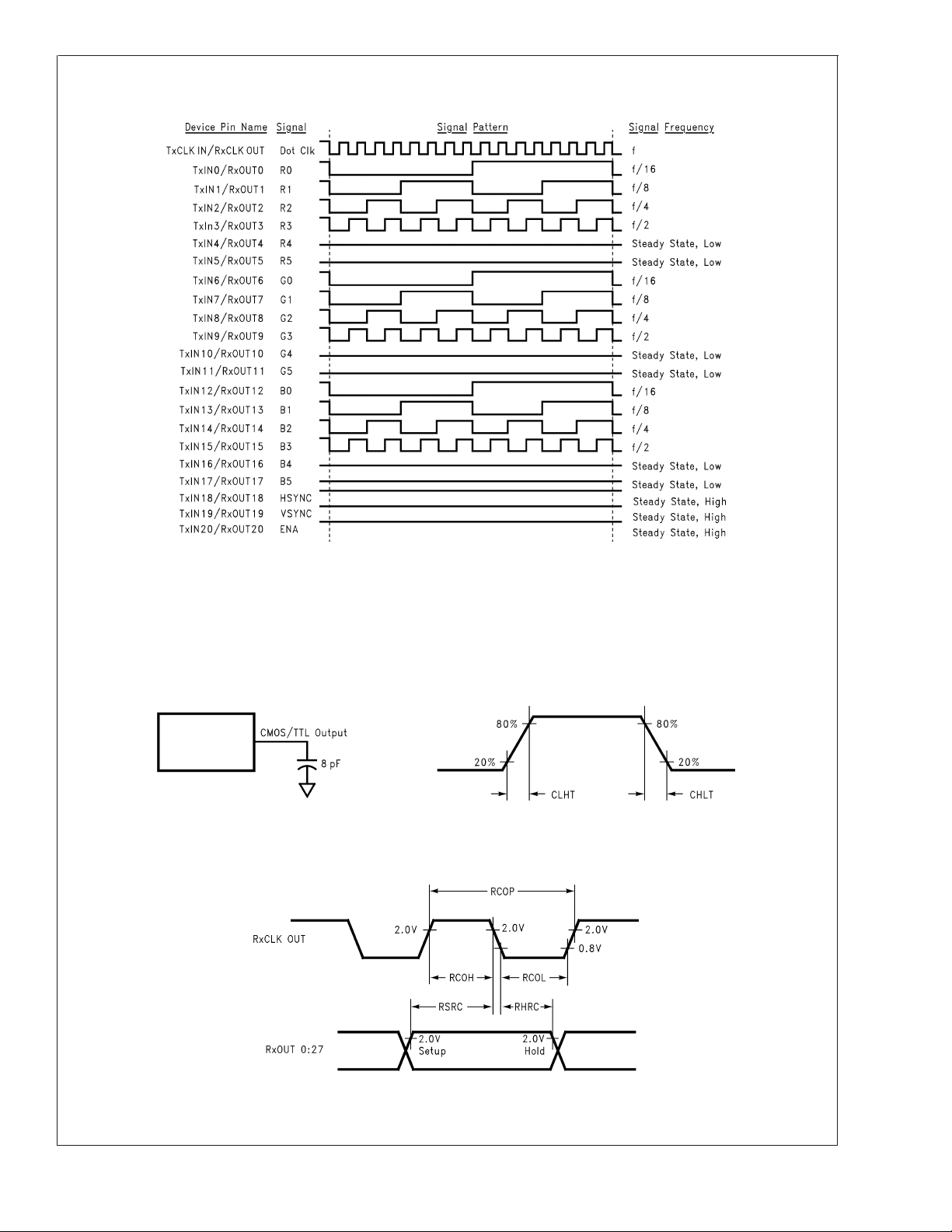
FIGURE 1. “Worst Case” Test Pattern
FIGURE 2. “16 Grayscale” Test Pattern (DS90CF386)(Notes 5, 6, 7, 8)
www.national.com 4
10108512
AC Timing Diagrams (Continued)
DS90CF386/DS90CF366
10108503
FIGURE 3. “16 Grayscale” Test Pattern (DS90CF366)(Notes 5, 6, 7, 8)
Note 5: The worst case test pattern produces a maximum toggling of digital circuits, LVDS I/O and CMOS/TTL I/O.
Note 6: The 16 grayscale test pattern tests device power consumption for a “typical” LCD display pattern. The test pattern approximates signal switching needed
to produce groups of 16 vertical stripes across the display.
Note 7: Figures 1, 3 show a falling edge data strobe (TxCLK IN/RxCLK OUT).
Note 8: Recommended pin to signal mapping. Customer may choose to define differently.
10108504
FIGURE 4. DS90CF386/DS90CF366 (Receiver) CMOS/TTL Output Load and Transition Times
10108505
FIGURE 5. DS90CF386/DS90CF366 (Receiver) Setup/Hold and High/Low Times
www.national.com5

AC Timing Diagrams (Continued)
DS90CF386/DS90CF366
FIGURE 6. DS90CF386/DS90CF366 (Receiver) Clock In to Clock Out Delay
FIGURE 7. DS90CF386/DS90CF366 (Receiver) Phase Lock Loop Set Time
10108506
10108507
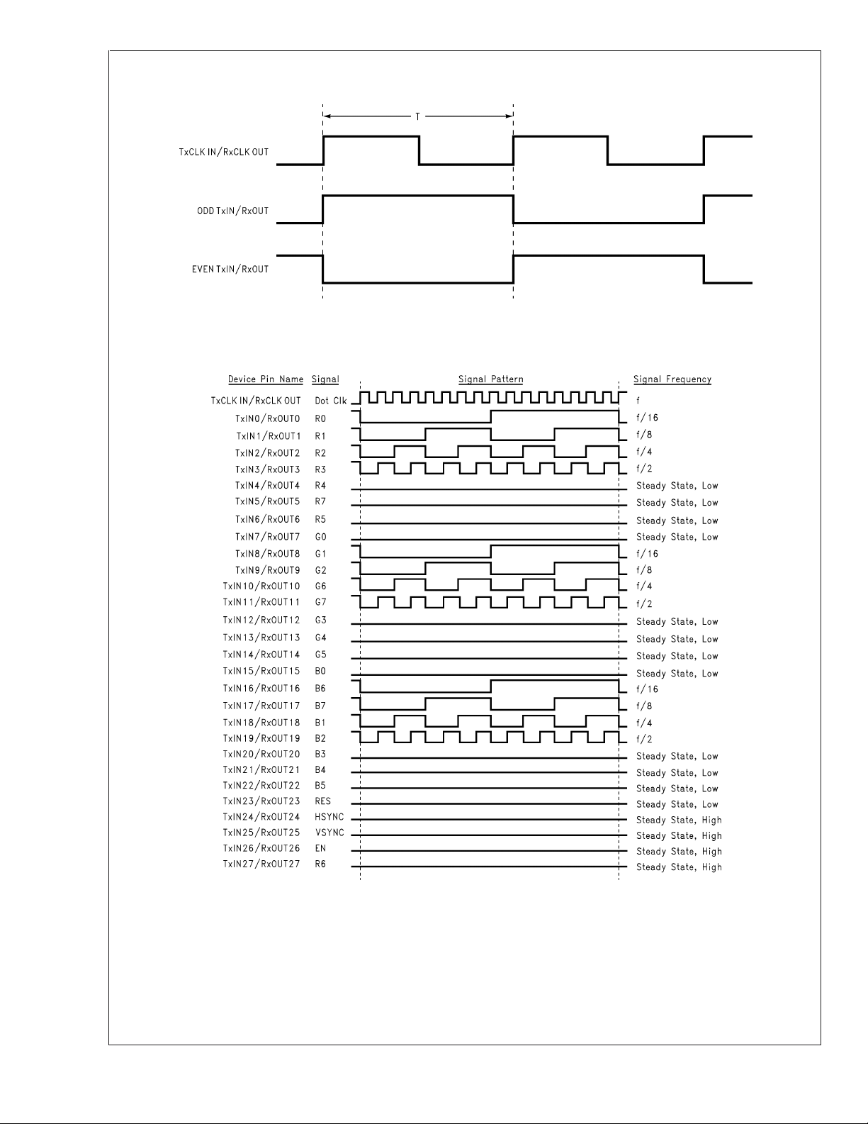
FIGURE 8. 28 Parallel TTL Data Inputs Mapped to LVDS Outputs - DS90CF386
www.national.com 6
10108509

AC Timing Diagrams (Continued)
FIGURE 9. 21 Parallel TTL Data Inputs Mapped to LVDS Outputs - DS90CF366
DS90CF386/DS90CF366
10108510
FIGURE 10. DS90CF386/DS90CF366 (Receiver) Power Down Delay
10108508
www.national.com7

AC Timing Diagrams (Continued)
DS90CF386/DS90CF366
FIGURE 11. DS90CF386 (Receiver) LVDS Input Strobe Position
www.national.com 8
10108525

AC Timing Diagrams (Continued)
DS90CF386/DS90CF366
FIGURE 12. DS90CF366 (Receiver) LVDS Input Strobe Position
10108526
www.national.com9

AC Timing Diagrams (Continued)
DS90CF386/DS90CF366
C —Setup and Hold Time (Internal data sampling window) defined by Rspos (receiver input strobe position) min and max
Tppos —Transmitter output pulse position (min and max)
RSKM = Cable Skew (type, length) + Source Clock Jitter (cycle to cycle) (Note 9) + ISI (Inter-symbol interference) (Note 10)
Cable Skew — typically 10 ps– 40 ps per foot, media dependent
Note 9: Cycle-to-cycle jitter is less than 250 ps at 85 MHz.
Note 10: ISI is dependent on interconnect length; may be zero.
FIGURE 13. Receiver LVDS Input Skew Margin
10108511
www.national.com 10
DS90CF386 MTD56 Package Pin Description—24-Bit FPD Link Receiver
Pin Name I/O No. Description
RxIN+ I 4 Positive LVDS differentiaI data inputs.
RxIN− I 4 Negative LVDS differential data inputs.
RxOUT O 28 TTL level data outputs. This includes: 8 Red, 8 Green, 8 Blue, and 3 control
lines — FPLINE, FPFRAME, DRDY (also referred to as HSYNC, VSYNC, Data
Enable).
RxCLK IN+ I 1 Positive LVDS differential clock input.
RxCLK IN− I 1 Negative LVDS differential clock input.
RxCLK OUT O 1 TTL Ievel clock output. The falling edge acts as data strobe.
PWR DOWN
V
CC
I 1 TTL level input. When asserted (low input) the receiver outputs are low.
I 4 Power supply pins for TTL outputs.
GND I 5 Ground pins for TTL outputs.
PLL V
CC
I 1 Power supply for PLL.
PLL GND I 2 Ground pin for PLL.
LVDS V
CC
I 1 Power supply pin for LVDS inputs.
LVDS GND I 3 Ground pins for LVDS inputs.
DS90CF366 MTD48 Package Pin Description—18-Bit FPD Link Receiver
Pin Name I/O No. Description
RxIN+ I 3 Positive LVDS differentiaI data inputs.
RxIN− I 3 Negative LVDS differential data inputs.
RxOUT O 21 TTL level data outputs. This includes: 6 Red, 6 Green, 6 Blue, and 3 control lines — FPLINE,
FPFRAME, DRDY (also referred to as HSYNC, VSYNC, Data Enable).
RxCLK IN+ I 1 Positive LVDS differential clock input.
RxCLK IN− I 1 Negative LVDS differential clock input.
RxCLK OUT O 1 TTL Ievel clock output. The falling edge acts as data strobe.
PWR DOWN
V
CC
GND I 5 Ground pins for TTL outputs.
PLL V
CC
PLL GND I 2 Ground pin for PLL.
LVDS V
CC
LVDS GND I 3 Ground pins for LVDS inputs.
I 1 TTL level input. When asserted (low input) the receiver outputs are low.
I 4 Power supply pins for TTL outputs.
I 1 Power supply for PLL.
I 1 Power supply pin for LVDS inputs.
DS90CF386/DS90CF366
DS90CF386 — 64 ball FBGA package Pin Description —
FPD Link Receiver
Pin Name I/O No. Description
RxIN+ I 4 Positive LVDS differentiaI data inputs.
RxIN− I 4 Negative LVDS differential data inputs.
RxOUT O 28 TTL level data outputs. This includes: 8 Red, 8 Green, 8 Blue, and 4 control lines — FPLINE,
FPFRAME, DRDY (also referred to as HSYNC, VSYNC, Data Enable).
RxCLK IN+ I 1 Positive LVDS differential clock input.
RxCLK IN− I 1 Negative LVDS differential clock input.
FPSHIFT OUT O 1 TTL Ievel clock output. The falling edge acts as data strobe. Pin name RxCLK OUT.
PWR DOWN
V
CC
GND I 5 Ground pins for TTL outputs.
PLL V
CC
PLL GND I 2 Ground pin for PLL.
LVDS V
CC
I 1 TTL level input. When asserted (low input) the receiver outputs are low.
I 4 Power supply pins for TTL outputs.
I 1 Power supply for PLL.
I 1 Power supply pin for LVDS inputs.
www.national.com11

DS90CF386 — 64 ball FBGA package Pin Description —
FPD Link Receiver
Pin Name I/O No. Description
LVDS GND I 3 Ground pins for LVDS inputs.
NC 6 Pins not connected.
(Continued)
DS90CF386 Pin Description — 64 ball FBGA Package —
DS90CF386/DS90CF366
FPD Link Receiver
By Pin By Pin Type
Pin Pin Name Type Pin Pin Name Type
A1 RxOUT17 O A4 GND G
A2 VCC P B1 GND G
A3 RxOUT15 O B6 GND G
A4 GND G D8 GND G
A5 RxOUT12 O E3 GND G
A6 RxOUT8 O E5 LVDS GND G
A7 RxOUT7 O G3 LVDS GND G
A8 RxOUT6 O G7 LVDS GND G
B1 GND G H5 LVDS GND G
B2 NC F6 PLL GND G
B3 RxOUT16 O G8 PLL GND G
B4 RxOUT11 O E6 PWR DWN I
B5 VCC P H6 RxCLKIN- I
B6 GND G H7 RxCLKIN+ I
B7 RxOUT5 O H2 RxIN0- I
B8 RxOUT3 O H3 RxIN0+ I
C1 RxOUT21 O F4 RxIN1- I
C2 NC G4 RxIN1+ I
C3 RxOUT18 O G5 RxIN2- I
C4 RxOUT14 O F5 RxIN2+ I
C5 RxOUT9 O G6 RxIN3- I
C6 RxOUT4 O H8 RxIN3+ I
C7 NC E7 RxCLKOUT O
C8 RxOUT1 O E8 RxOUT0 O
D1 VCC P C8 RxOUT1 O
D2 RxOUT20 O D5 RxOUT10 O
D3 RxOUT19 O B4 RxOUT11 O
D4 RxOUT13 O A5 RxOUT12 O
D5 RxOUT10 O D4 RxOUT13 O
D6 VCC P C4 RxOUT14 O
D7 RxOUT2 O A3 RxOUT15 O
D8 GND G B3 RxOUT16 O
E1 RxOUT22 O A1 RxOUT17 O
E2 RxOUT24 O C3 RxOUT18 O
E3 GND G D3 RxOUT19 O
E4 LVDS VCC P D7 RxOUT2 O
E5 LVDS GND G D2 RxOUT20 O
E6 PWR DWN I C1 RxOUT21 O
E7 RxCLKOUT O E1 RxOUT22 O
E8 RxOUT0 O F1 RxOUT23 O
www.national.com 12

DS90CF386 Pin Description — 64 ball FBGA Package —
FPD Link Receiver
F1 RxOUT23 O E2 RxOUT24 O
F2 RxOUT26 O G1 RxOUT25 O
F3 NC F2 RxOUT26 O
F4 RxIN1- I H1 RxOUT27 O
F5 RxIN2+ I B8 RxOUT3 O
F6 PLL GND G C6 RxOUT4 O
F7 PLL VCC P B7 RxOUT5 O
F8 NC A8 RxOUT6 O
G1 RxOUT25 O A7 RxOUT7 O
G2 NC A6 RxOUT8 O
G3 LVDS GND G C5 RxOUT9 O
G4 RxIN1+ I E4 LVDS VCC P
G5 RxIN2- I H4 LVDS VCC P
G6 RxIN3- I F7 PLL VCC P
G7 LVDS GND G A2 VCC P
G8 PLL GND G B5 VCC P
H1 RxOUT27 O D1 VCC P
H2 RxIN0- I D6 VCC P
H3 RxIN0+ I B2 NC
H4 LVDS VCC P C2 NC
H5 LVDS GND G C7 NC
H6 RxCLKIN- I F3 NC
H7 RxCLKIN+ I F8 NC
H8 RxIN3+ I G2 NC
G: Ground
I : Input
O: Output
P: Power
NC: Not connectted
(Continued)
By Pin By Pin Type
DS90CF386/DS90CF366
www.national.com13

Pin Diagrams for TSSOP Packages
DS90CF386MTD DS90CF366MTD
DS90CF386/DS90CF366
10108513
10108523
Applications Information
POWER SEQUENCING AND POWERDOWN MODE
Outputs of the transmitter remain in TRI-STATE until the
power supply reaches 2V. Clock and data outputs will begin
to toggle 10 ms after V
down pin is above 1.5V. Either device may be placed into a
powerdown mode at any time by asserting the Powerdown
pin (active low). Total power dissipation for each device will
decrease to 5 µW (typical).
The transmitter input clock may be applied prior to powering
up and enabling the transmitter. The transmitter input clock
may also be applied after power up; however, the use of the
PWR DOWN pin is required as described in the Transmitter
Input Clock section. Do not power up and enable (PWR
DOWN = HIGH) the transmitter without a valid clock signal
applied to the TxCLK IN pin.
The FPD Link chipset is designed to protect itself from
accidental loss of power to either the transmitter or receiver.
If power to the transmit board is lost, the receiver clocks
(input and output) stop. The data outputs (RxOUT) retain the
states they were in when the clocks stopped. When the
has reached 3V and the Power-
CC
receiver board loses power, the receiver inputs are controlled by a failsafe bias circuitry. The LVDS inputs are
High-Z during initial power on and power off conditions.
Current is limited (5 mA per input) by the fixed current mode
drivers, thus avoiding the potential for latchup when powering the device.
RECEIVER FAILSAFE FEATURE
The FPD Link receivers have input failsafe bias circuitry to
guarantee a stable receiver output for floating or terminated
receiver inputs. Under these conditions receiver inputs will
be pulled to a HIGH state. This is the case if not all data
channels are required in the application. Leave the extra
channel’s inputs open. This minimizes power dissipation and
locks the unused channels outputs into a stable known
(HIGH) state.
If a clock signal is present, data outputs will all be HIGH; if
the clock input is also floating/terminated, data outputs will
remain in the last valid state. A floating/terminated clock
input will result in a LOW clock output.
www.national.com 14

Physical Dimensions inches (millimeters) unless otherwise noted
DS90CF386/DS90CF366
56-Lead Molded Thin Shrink Small Outline Package, JEDEC
Dimensions shown in millimeters only
Order Number DS90CF386MTD
NS Package Number MTD56
48-Lead Molded Thin Shrink Small Outline Package, JEDEC
Dimensions shown in millimeters only
Order Number DS90CF366MTD
NS Package Number MTD48
www.national.com15

Physical Dimensions inches (millimeters) unless otherwise noted (Continued)
64 ball, 0.8mm fine pitch ball grid array (FBGA) Package
Dimensions show in millimeters
Order Number DS90CF386SLC
NS Package Number SLC64A
LIFE SUPPORT POLICY
NATIONAL’S PRODUCTS ARE NOT AUTHORIZED FOR USE AS CRITICAL COMPONENTS IN LIFE SUPPORT
DEVICES OR SYSTEMS WITHOUT THE EXPRESS WRITTEN APPROVAL OF THE PRESIDENT AND GENERAL
COUNSEL OF NATIONAL SEMICONDUCTOR CORPORATION. As used herein:
2. A critical component is any component of a life
support device or system whose failure to perform
can be reasonably expected to cause the failure of
the life support device or system, or to affect its
safety or effectiveness.
DS90CF386/DS90CF366 +3.3V LVDS Receiver 24-Bit-Color Flat Panel Display (FPD)
1. Life support devices or systems are devices or
systems which, (a) are intended for surgical implant
into the body, or (b) support or sustain life, and
whose failure to perform when properly used in
accordance with instructions for use provided in the
labeling, can be reasonably expected to result in a
significant injury to the user.
Link—85 MHz, +3.3V LVDS Receiver 18-Bit-Color Flat Panel Display (FPD) Link—85 MHz
National does not assume any responsibility for use of any circuitry described, no circuit patent licenses are implied and National reserves the right at any time without notice to change said circuitry and specifications.
National Semiconductor
Americas Customer
Support Center
Email: new.feedback@nsc.com
Tel: 1-800-272-9959
www.national.com
National Semiconductor
Europe Customer Support Center
Fax: +49 (0) 180-530 85 86
Email: europe.support@nsc.com
Deutsch Tel: +49 (0) 69 9508 6208
English Tel: +44 (0) 870 24 0 2171
Français Tel: +33 (0) 1 41 91 8790
National Semiconductor
Asia Pacific Customer
Support Center
Email: ap.support@nsc.com
National Semiconductor
Japan Customer Support Center
Fax: 81-3-5639-7507
Email: jpn.feedback@nsc.com
Tel: 81-3-5639-7560
 Loading...