

January 2000
DS90CF363
+3.3V LVDS Transmitter 18-Bit Flat Panel Display (FPD)
Link—65 MHz
DS90CF363 +3.3V LVDS Transmitter 18-Bit Flat Panel Display (FPD) Link—65 MHz
General Description
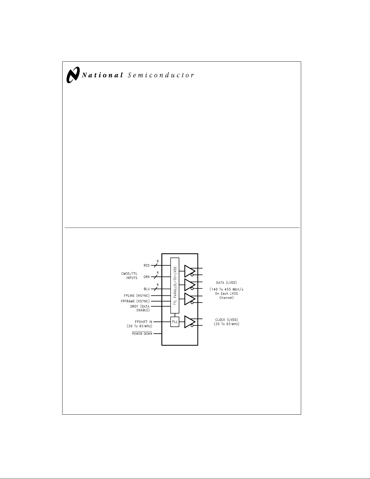
The DS90CF363 transmitter converts 21 bits of CMOS/TTL
data into three LVDS (Low Voltage Differential Signaling)
data streams. A phase-lockedtransmit clock is transmitted in
parallel with the data streams over a fourth LVDSlink. Every
cycle of the transmit clock 21 bits of input data are sampled
and transmitted. At a transmit clock frequency of 65 MHz, 18
bits of RGB data and 3 bits of LCD timing and control data
(FPLINE, FPFRAME, DRDY) are transmitted at arate of 455
Mbps per LVDS data channel. Using a 65 MHz clock, the
data throughputs is 170 Mbytes/sec.
This chipset is an ideal means to solve EMI and cable size
problems associated with wide, high speed TTL interfaces.
Block Diagram
DS90CF363
Features
n 20 to 65 MHz shift clock support
n Single 3.3V supply
n Chipset (Tx + Rx) power consumption
n Power-down mode (
n Single pixel per clock XGA (1024x768) ready
n Supports VGA, SVGA, XGA and higher addressability.
n Up to 170 Megabytes/sec bandwidth
n Up to 1.3 Gbps throughput
n Narrow bus reduces cable size and cost
n 290 mV swing LVDS devices for low EMI
n PLL requires no external components
n Low profile 48-lead TSSOP package
n Falling edge data strobe Transmitter
n Compatible with TIA/EIA-644 LVDS standard
n ESD rating
n Operating Temperature: −40˚C to +85˚C
>
7kV
<
0.5 mW total)
<
250 mW (typ)
DS100032-1
Order Number DS90CF363MTD
See NS Package Number MTD48
TRI-STATE®is a registered trademark of National Semiconductor Corporation.
© 2000 National Semiconductor Corporation DS100032 www.national.com
Absolute Maximum Ratings (Note 1)
If Military/Aerospace specified devices are required,
please contact the National SemiconductorSales Office/
Distributors for availability and specifications.
DS90CF363
Supply Voltage (V
CMOS/TTL Input Voltage −0.3V to (V
LVDS Driver Output Voltage −0.3V to (V
LVDS Output Short Circuit
Duration Continuous
Junction Temperature +150˚C
Storage Temperature −65˚C to +150˚C
Lead Temperature
(Soldering, 4 sec) +260˚C
Maximum Package Power Dissipation Capacity
MTD48 (TSSOP) Package:
DS90CF363 1.98 W
) −0.3V to +4V
CC
CC
CC
@
+ 0.3V)
+ 0.3V)
25˚C
Package Derating:
DS90CF363 16 mW/˚C above +25˚C
ESD Rating
(HBM, 1.5 kΩ, 100 pF)
Recommended Operating
Conditions
Supply Voltage (V
) 3.0 3.3 3.6 V
CC
Operating Free Air
Temperature (T
) −40 +25 +85 ˚C
A
Receiver Input Range 0 2.4 V
Supply Noise Voltage (V
Min Nom Max Units
) 100 mV
CC
Electrical Characteristics
Over recommended operating supply and temperature ranges unless otherwise specified.
Symbol Parameter Conditions Min Typ Max Units
CMOS/TTL DC SPECIFICATIONS
V
IH
V
IL
V
OH
V
OL
V
CL
I
IN
I
OS
LVDS DC SPECIFICATIONS
V
OD
∆V
V
OS
∆V
I
OS
I
OZ
V
TH
V
TL
I
IN
TRANSMITTER SUPPLY CURRENT
ICCTW Transmitter Supply Current
ICCTG Transmitter Supply Current
ICCTZ Transmitter Supply Current
Note 1: “Absolute Maximum Ratings” are those values beyond which the safety of the device cannot be guaranteed. They are not meant to imply that the device
should be operated at these limits. The tables of “Electrical Characteristics” specify conditions for device operation.
High Level Input Voltage 2.0 V
Low Level Input Voltage GND 0.8 V
High Level Output Voltage IOH= −0.4 mA 2.7 3.3 V
Low Level Output Voltage IOL= 2 mA 0.1 0.3 V
Input Clamp Voltage ICL= −18 mA −0.79 −1.5 V
Input Current VIN=VCC, GND, 2.5V or 0.4V
Output Short Circuit Current V
= 0V −60 −120 mA
OUT
±
5.1±10 µA
Differential Output Voltage RL= 100Ω 250 345 450 mV
Change in VODbetween
OD
complimentary output states
Offset Voltage (Note 4) 1.125 1.25 1.375 V
Change in VOSbetween
OS
complimentary output states
Output Short Circuit Current V
Output TRI-STATE®Current Power Down = 0V,
= 0V, RL= 100Ω −3.5 −5 mA
OUT
V
OUT
=0VorV
CC
±
1
Differential Input High Threshold VCM= +1.2V +100 mV
Differential Input Low Threshold −100 mV
Input Current VIN= +2.4V, VCC= 3.6V
V
= 0V, VCC= 3.6V
IN
R
Worst Case
16 Grayscale
Power Down
= 100Ω,
L
= 5 pF,
C
L
Worst Case Pattern
(Figures 1, 3)
R
= 100Ω,
L
= 5 pF,
C
L
16 Grayscale Pattern
(Figures 2, 3)
Power Down = Low
Driver Outputs in TRI-STATE®under
f = 32.5 MHz 31 45 mA
f = 37.5 MHz 32 50 mA
f = 65 MHz 42 55 mA
f = 32.5 MHz 23 35 mA
f = 37.5 MHz 28 40 mA
f = 65 MHz 31 45 mA
10 55 µA
Power Down Mode
CC
35 mV
35 mV
±
10 µA
±
10 µA
±
10 µA
>
7kV
PP
V
www.national.com 2
Electrical Characteristics (Continued)
Note 2: Typical values are given for VCC= 3.3V and TA= +25C.
Note 3: Current into device pins is defined as positive. Current out of device pins is defined as negative. Voltages are referenced to ground unless otherwisespeci-
fied (except V
Note 4: V
and ∆VOD).
OD
previously referred as VCM.
OS
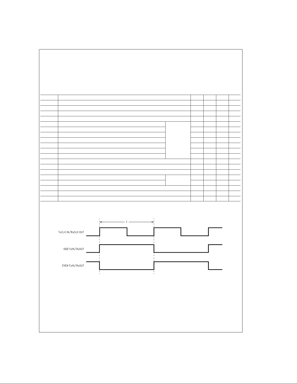
Transmitter Switching Characteristics
Over recommended operating supply and temperature ranges unless otherwise specified
Symbol Parameter Min Typ Max Units
(Figure 4 )
(Figure 3 )
(Figure 3 )
(Figure 5 )
(Figure 12)
f = 65 MHz −0.4 0 0.3 ps
LLHT LVDS Low-to-High Transition Time
LHLT LVDS High-to-Low Transition Time
TCIT TxCLK IN Transition Time
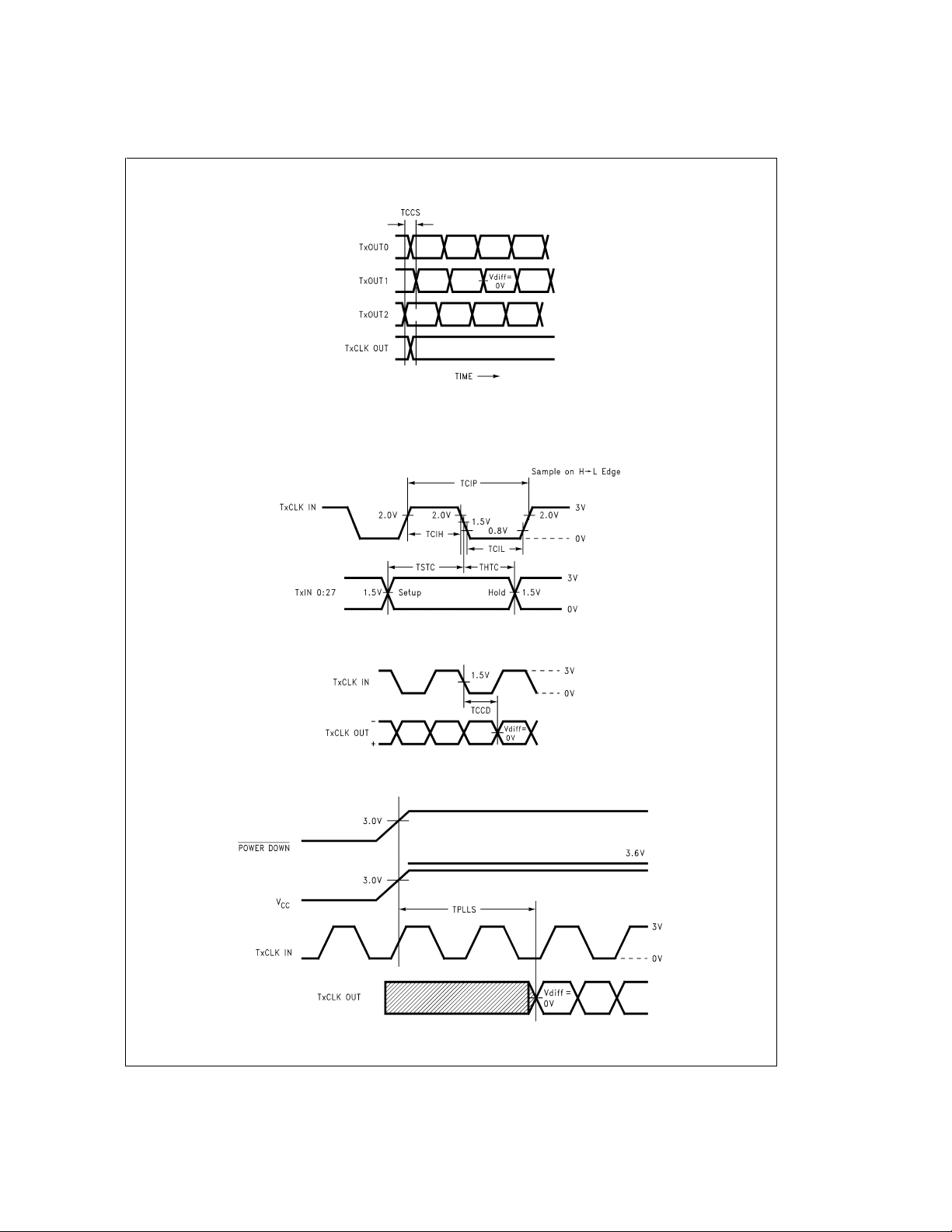
TCCS TxOUT Channel-to-Channel Skew
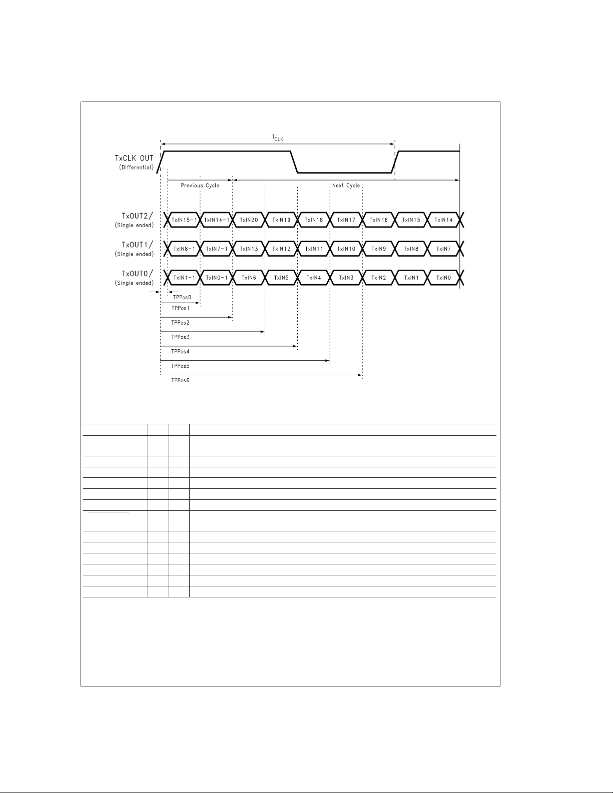
TPPos0 Transmitter Output Pulse Position for Bit 0
TPPos1 Transmitter Output Pulse Position for Bit 1 1.8 2.2 2.5 ns
TPPos2 Transmitter Output Pulse Position for Bit 2 4.0 4.4 4.7 ns
TPPos3 Transmitter Output Pulse Position for Bit 3 6.2 6.6 6.9 ns
TPPos4 Transmitter Output Pulse Position for Bit 4 8.4 8.8 9.1 ns
TPPos5 Transmitter Output Pulse Position for Bit 5 10.6 11.0 11.3 ns
TPPos6 Transmitter Output Pulse Position for Bit 6 12.8 13.2 13.5 ns
TCIP TxCLK IN Period
TCIH TxCLK IN High Time
TCIL TxCLK IN Low Time
TSTC TxIN Setup to TxCLK IN
THTC TxIN Hold to TxCLK IN
TCCD TxCLK IN to TxCLK OUT Delay 25˚C, V
TPLLS Transmitter Phase Lock Loop Set
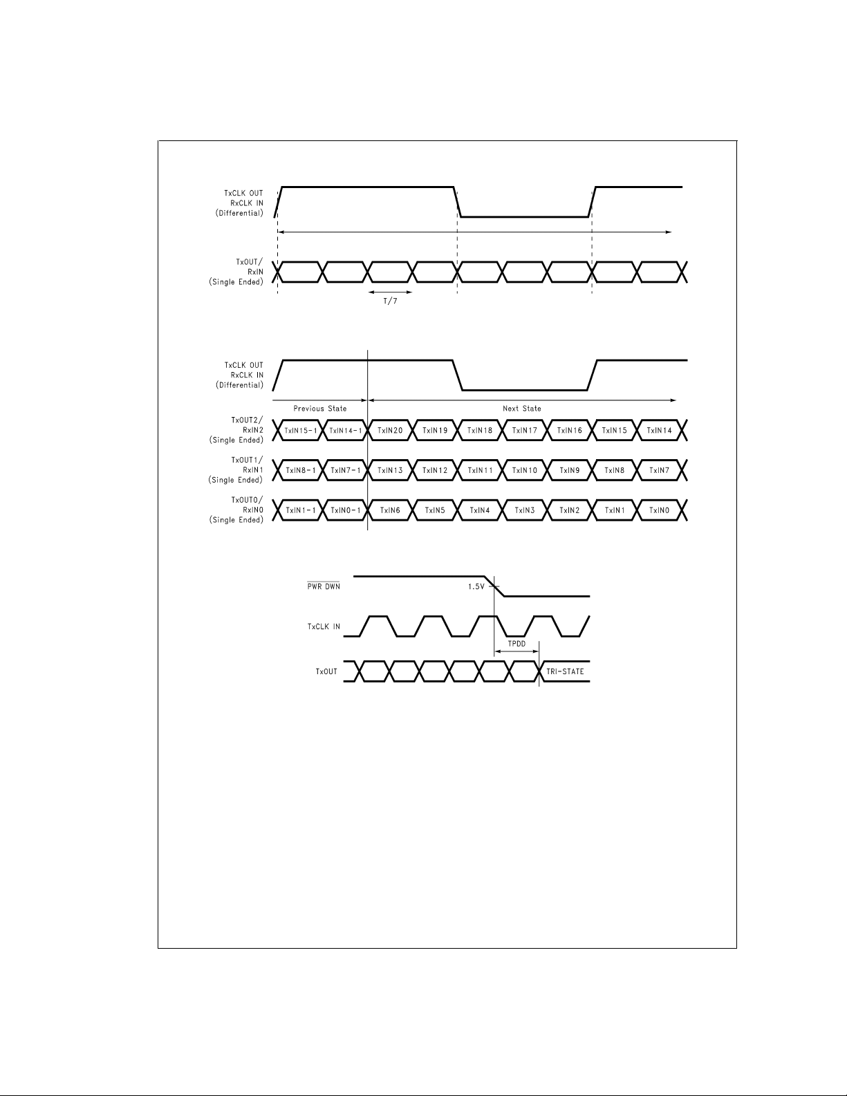
TPDD Transmitter Power Down Delay
(Figure 6)
(Figure 6)
(Figure 6)
(Figure 6)
(Figure 6)
(Figure 11)
CC
(Figure 8 )
= 3.3V
0.35T 0.5T 0.65T ns
0.35T 0.5T 0.65T ns
f = 65 MHz 2.5 ns
(Figure 7 )
0.75 1.5 ns
0.75 1.5 ns
5ns
250 ps
15 T 50 ns
0ns
3 5.5 ns
10 ms
100 ns
DS90CF363
AC Timing Diagrams
DS100032-4
FIGURE 1. “Worst Case” Test Pattern
www.national.com3
AC Timing Diagrams (Continued)
DS90CF363
DS100032-5
FIGURE 2. “16 Grayscale” Test Pattern (Notes 5, 6, 7, 8)
Note 5: The worst case test pattern produces a maximum toggling of digital circuits, LVDS I/O and CMOS/TTL I/O.
Note 6: The 16 grayscale test pattern tests device power consumption for a “typical” LCD display pattern. The test pattern approximates signal switching needed
to produce groups of 16 vertical stripes across the display.
Note 7:
Figures 1, 2
Note 8: Recommended pin to signal mapping. Customer may choose to define differently.
show a falling edge data strobe (TxCLK IN/RxCLK OUT).
FIGURE 3. DS90CF363 (Transmitter) LVDS Output Load and Transition Times
FIGURE 4. DS90CF363 (Transmitter) Input Clock Transition Time
www.national.com 4
DS100032-6
DS100032-8
AC Timing Diagrams (Continued)
DS90CF363
Measurements at V
TCCS measured between earliest and latest LVDS edges
TxCLK Differential Low→High Edge
=0V
diff
FIGURE 5. DS90CF363 (Transmitter) Channel-to-Channel Skew
FIGURE 6. DS90CF363 (Transmitter) Setup/Hold and High/Low Times
FIGURE 7. DS90CF363 (Transmitter) Clock In to Clock Out Delay
DS100032-9
DS100032-10
DS100032-12
FIGURE 8. DS90CF363 (Transmitter) Phase Lock Loop Set Time
DS100032-14
www.national.com5
AC Timing Diagrams (Continued)
DS90CF363
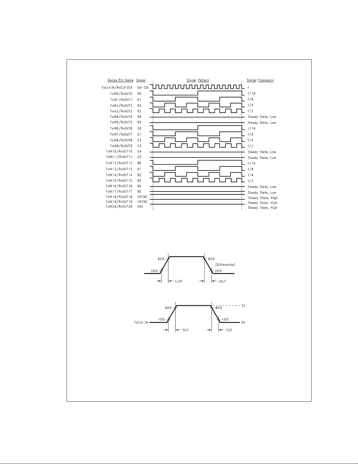
FIGURE 10. 21 Parallel TTL Data Inputs Mapped to LVDS Outputs
DS100032-16
FIGURE 9. Seven Bits of LVDS in One Clock Cycle
DS100032-17
FIGURE 11. Transmitter Power Down Delay
www.national.com 6
DS100032-18
AC Timing Diagrams (Continued)
FIGURE 12. Transmitter LVDS Output Pulse Position Measurement
DS90CF363 Pin Description—FPD Link Transmitter
DS90CF363
DS100032-20
Pin Name I/O No. Description
TxIN I 21 TTL level input. This includes: 6 Red, 6 Green, 6 Blue, and 3 control lines— FPLINE,
FPFRAME and DRDY (also referred to as HSYNC, VSYNC, Data Enable).
TxOUT+ O 3 Positive LVDS differentiaI data output.
TxOUT− O 3 Negative LVDS differential data output.
FPSHIFT IN I 1 TTL Ievel clock input. The falling edge acts as data strobe. Pin name TxCLK IN.
TxCLK OUT+ O 1 Positive LVDS differential clock output.
TxCLK OUT− O 1 Negative LVDS differential clock output.
PWR DOWN
I 1 TTL level input. When asserted (low input) TRI-STATES the outputs, ensuring low current at
power down.
V
CC
I 4 Power supply pins for TTL inputs.
GND I 4 Ground pins for TTL inputs.
PLL V
CC
I 1 Power supply pin for PLL.
PLL GND I 2 Ground pins for PLL.
LVDS V
CC
I 1 Power supply pin for LVDS outputs.
LVDS GND I 3 Ground pins for LVDS outputs.
Applications Information
The DS90CF363 and DS90CF364 are backward compatible
with the existing 5V FPD Link transmitter/receiver pair
(DS90CF563 and DS90CF564). To upgrade from a 5V to a
3.3V system the following must be addressed:
1. Change 5V power supply to 3.3V. Provide this supply to
the V
, LVDS VCCand PLLVCCof both the transmitter
CC
and receiver devices. This change may enable the removal of a 5V supply from the system, and power may
be supplied from an existing 3V power source.
2. The DS90CF363 transmitter input and control inputs accept 3.3V TTL/CMOS levels. They are not 5V tolerant.
www.national.com7
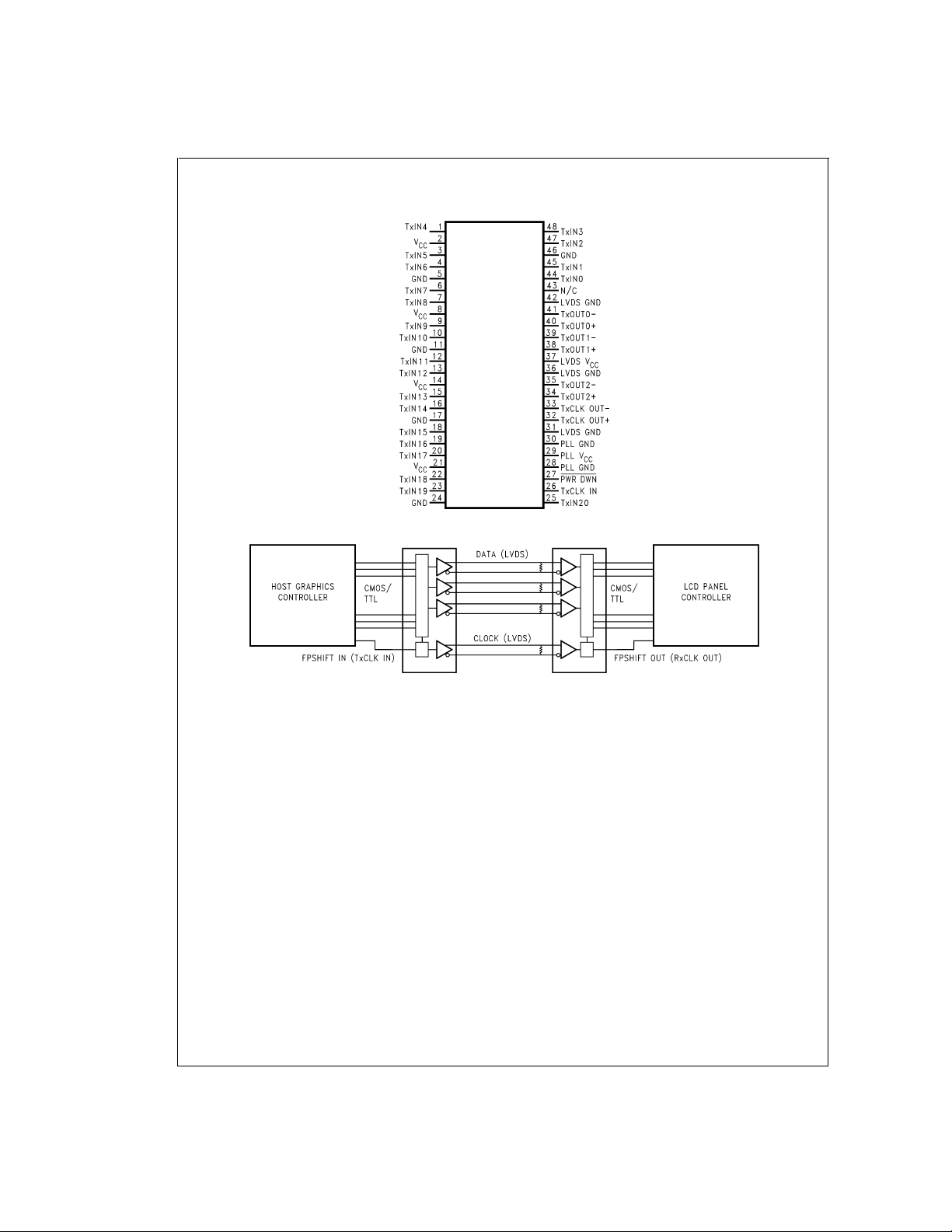
Pin Diagram
DS90CF363
DS90CF363
DS100032-23
Application
www.national.com 8
DS100032-3

Physical Dimensions inches (millimeters) unless otherwise noted
DS90CF363 +3.3V LVDS Transmitter 18-Bit Flat Panel Display (FPD) Link—65 MHz
48-Lead Molded Thin Shrink Small Outline Package, JEDEC
Order Number DS90CF363MTD
NS Package Number MTD48
LIFE SUPPORT POLICY
NATIONAL’S PRODUCTS ARE NOT AUTHORIZED FOR USE AS CRITICAL COMPONENTS IN LIFE SUPPORT
DEVICES OR SYSTEMS WITHOUT THE EXPRESS WRITTEN APPROVAL OF THE PRESIDENT AND GENERAL
COUNSEL OF NATIONAL SEMICONDUCTOR CORPORATION. As used herein:
1. Life support devices or systems are devices or
systems which, (a) are intended for surgical implant
into the body, or (b) support or sustain life, and
whose failure to perform when properly used in
accordance with instructions for use provided in the
2. A critical component is any component of a life
support device or system whose failure to perform
can be reasonably expected to cause the failure of
the life support device or system, or to affect its
safety or effectiveness.
labeling, can be reasonably expected to result in a
significant injury to the user.
National Semiconductor
Corporation
Americas
Tel: 1-800-272-9959
Fax: 1-800-737-7018
Email: support@nsc.com
www.national.com
National Semiconductor
Europe
Fax: +49 (0) 1 80-530 85 86
Email: europe.support@nsc.com
Deutsch Tel: +49 (0) 1 80-530 85 85
English Tel: +49 (0) 1 80-532 78 32
Français Tel: +49 (0) 1 80-532 93 58
Italiano Tel: +49 (0) 1 80-534 16 80
National Semiconductor
Asia Pacific Customer
Response Group
Tel: 65-2544466
Fax: 65-2504466
Email: sea.support@nsc.com
National Semiconductor
Japan Ltd.
Tel: 81-3-5639-7560
Fax: 81-3-5639-7507
National does not assume any responsibility for use of any circuitry described, no circuit patent licenses are implied and National reserves the right at any time without notice to change said circuitry and specifications.
 Loading...