

National Semiconductor DS90C402 Technical data
查询DS90C402供应商
DS90C402
Dual Low Voltage Differential Signaling (LVDS) Receiver
DS90C402 Dual Low Voltage Differential Signaling (LVDS) Receiver
June 1998
General Description
The DS90C402 is a dual receiver device optimized for high
data rate and low power applications. This device along with
the DS90C401 provides a pair chip solution for a dual high
speed point-to-point interface. The device is in a PCB space
saving 8 lead small outline package. The receiver offers
±
100 mV threshold sensitivity, in addition to common-mode
noise protection.
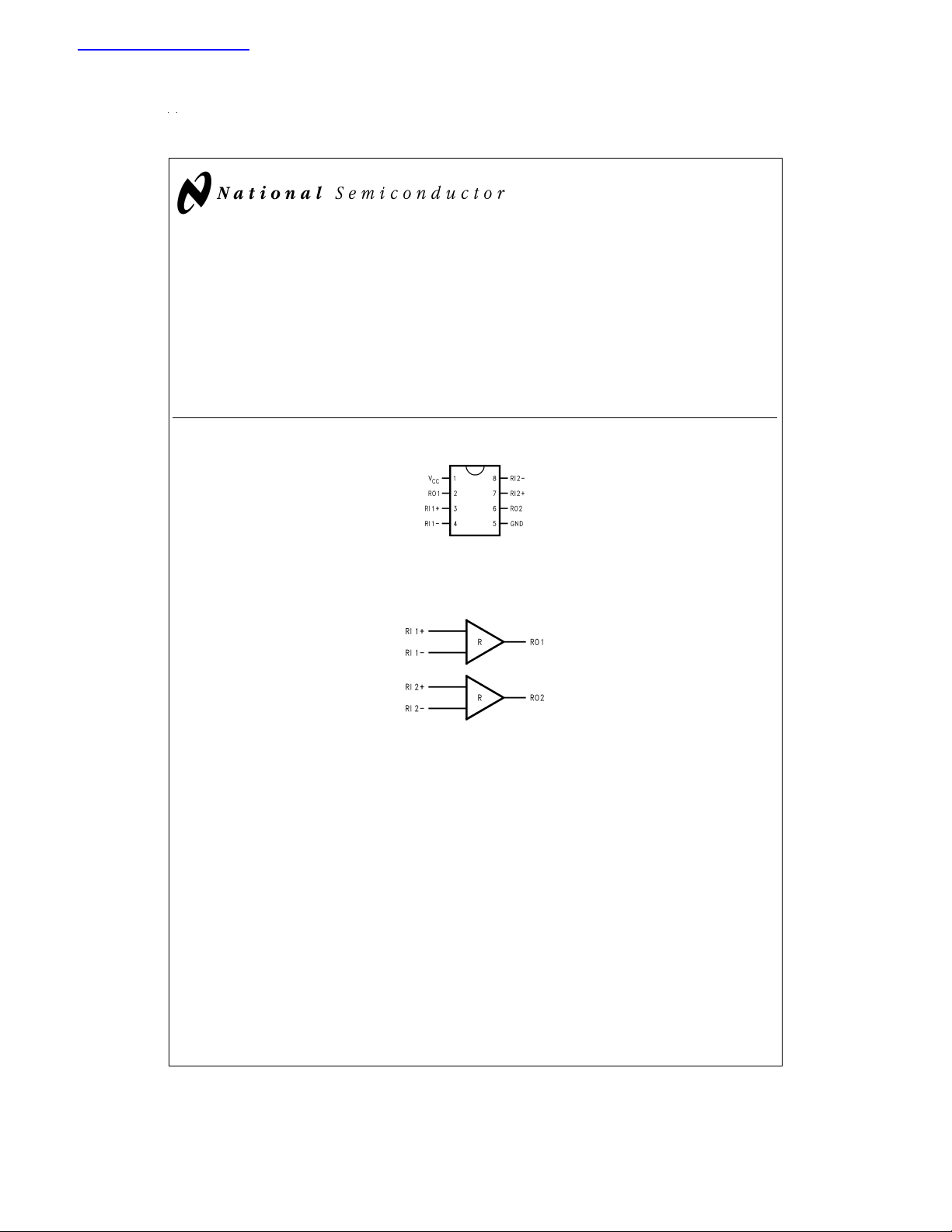
Connection Diagram
Order Number DS90C402M
See NS Package Number M08A
Functional Diagram
Features
n Ultra Low Power Dissipation
n Operates above 155.5 Mbps
n Standard TIA/EIA-644
n 8 Lead SOIC Package saves PCB space
±
n V
1V center around 1.2V
CM
±
n
100 mV Receiver Sensitivity
DS100006-1
DS100006-2
TRI-STATE®is a registered trademark of National Semiconductor Corporation.
© 1998 National Semiconductor Corporation DS100006 www.national.com
Absolute Maximum Ratings (Note 1)
If Military/Aerospace specified devices are required,
please contact the National Semiconductor Sales Office/
Distributors for availability and specifications.
Supply Voltage (V
Input Voltage (R
Output Voltage (R
Maximum Package Power Dissipation
M Package 1025 mW
Derate M Package 8.2 mW/˚C above +25˚C
Storage Temperature Range −65˚C to +150˚C
Lead Temperature Range
Soldering (4 sec.) +260˚C
) −0.3V to +6V
CC
) −0.3V to (VCC+ 0.3V)
IN+,RIN−
) −0.3V to (VCC+ 0.3V)
OUT
@
+25˚C
Maximum Junction Temperature +150˚C
ESD Rating (Note 4)
(HBM, 1.5 kΩ, 100 pF) ≥ 3,500V
(EIAJ, 0 Ω, 200 pF) ≥ 250V
Recommended Operating
Conditions
Supply Voltage (V
) +4.5 +5.0 +5.5 V
CC
Receiver Input Voltage GND 2.4 V
Operating Free Air
Temperature (T
) −40 +25 +85 ˚C
A
Min Typ Max Units
Electrical Characteristics
Over Supply Voltage and Operating Temperature ranges, unless otherwise specified. (Note 2)
Symbol Parameter Conditions Pin Min Typ Max Units
V
V
I
V
V
I
I
Differential Input High Threshold VCM= + 1.2V R
TH
Differential Input Low Threshold −100 mV
TL
Input Current VIN= +2.4V VCC= 5.5V −10
IN
Output High Voltage IOH= −0.4 mA, VID= +200 mV R
OH
Output Low Voltage IOL= 2 mA, VID= −200 mV 0.07 0.3 V
OL
Output Short Circuit Current V
OS
No Load Supply Current Inputs Open V
CC
V
= 0V −10
IN
I
= −0.4mA, Inputs terminated 3.8 4.9 V
OH
I
= −0.4mA, Inputs Open 3.8 4.9 V
OH
I
= −0.4mA, Inputs Shorted 4.9 V
OH
= 0V (Note 8) −15 −60 −100 mA
OUT
,
IN+
R
IN−
3.8 4.9 V
OUT
CC
+100 mV
±
1 +10 µA
±
1 +10 µA
3.5 10 mA
Switching Characteristics
VCC= +5.0V±10%,TA= −40˚C to +85˚C (Notes 3, 4, 5, 6, 9)
Symbol Parameter Conditions Min Typ Max Units
t
t
t
t
t
t
t
www.national.com 2
Differential Propagation Delay High to Low CL= 5 pF,
PHLD
Differential Propagation Delay Low to High 1.0 3.48 6.0 ns
PLHD
Differential Skew |t
SKD
Channel-to-Channel Skew (Note 5) 0 0.6 1.5 ns
SK1
Chip to Chip Skew (Note 6) 5.0 ns
SK2
Rise Time 0.5 2.5 ns
TLH
Fall Time 0.5 2.5 ns
THL
PHLD−tPLHD
| 0 0.08 1.2 ns
= 200 mV
V
ID
Figure 1
(
and
Figure 2
1.0 3.40 6.0 ns
)
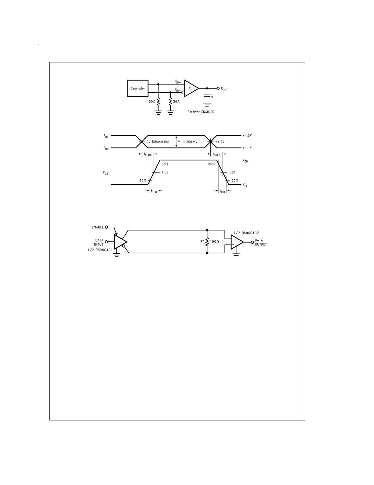
Parameter Measurement Information
FIGURE 1. Receiver Propagation Delay and Transition Time Test Circuit
FIGURE 2. Receiver Propagation Delay and Transition Time Waveforms
Typical Application
DS100006-4
DS100006-5
FIGURE 3. Point-to-Point Application
Applications Information
LVDSdriversandreceivers are intended to be primarily used
in an uncomplicated point-to-point configuration as is shown
in
Figure 3
vironment for the quick edge rates of the drivers. The receiver is connected to the driver through a balanced media
which may be a standard twisted pair cable, a parallel pair
cable, or simply PCB traces. Typically the characteristic impedance of the media is in the range of 100Ω. A termination
resistor of 100Ω should be selected to match the media, and
is located as close to the receiver input pins as possible. The
termination resistor converts the current sourced by the
driver into a voltage that is detected by the receiver. Other
configurations are possible such as a multi-receiver configuration, but the effects of a mid-stream connector(s), cable
stub(s), and other impedance discontinuities as well as
ground shifting, noise margin limits, and total termination
loading must be taken into account.
The DS90C402 differential line receiver is capable of detecting signals as low as 100 mV, over a
range centered around +1.2V.This is related to the driver offset voltage which is typically +1.2V.The driven signal is centered around this voltage and may shift
ter point. The
potential difference between the driver’s ground reference
and the receiver’s ground reference, the common-mode effects of coupled noise, or a combination of the two. Both re-
. This configuration provides a clean signaling en-
±
1V common-mode
±
±
1V shifting may be the result of a ground
1V around this cen-
DS100006-8
ceiver input pins should honor their specified operating input
voltage range of 0V to +2.4V (measured from each pin to
ground), exceeding these limits may turn on the ESD protection circuitry which will clamp the bus voltages.
Fail-Safe Feature:
The LVDS receiver is a high gain, high speed device that
amplifies a small differential signal (20mV) to CMOS logic
levels. Due to the high gain and tight threshold of the receiver,care should be taken to prevent noise from appearing
as a valid signal.
The receiver’s internal fail-safe circuitry is designed to
source/sink a small amount of current, providing fail-safe
protection (a stable known state HIGH output voltage) for
floating, terminated or shorted receiver inputs.
1. Open Input Pins. The DS90C402 is a dual receiver device, and if an application requires only one receiver,the
unused channel(s) inputs should be left OPEN. Do not
tie unused receiver inputs to ground or any other voltages. The input is biased by internal high value pull up
and pull down resistors to set the output to a HIGH state.
This internal circuitry will guarantee a HIGH, stable output state for open inputs.
www.national.com3
 Loading...