

查询DS90C401供应商
DS90C401
Dual Low Voltage Differential Signaling (LVDS) Driver
DS90C401 Dual Low Voltage Differential Signaling (LVDS) Driver
August 2005
General Description
The DS90C401 is a dual driver device optimized for high
data rate and low power applications. This device along with
the DS90C402 provides a pair chip solution for a dual high
speed point-to-point interface. The DS90C401 is a current
mode driver allowing power dissipation to remain low even at
high frequency. In addition, the short circuit fault current is
also minimized. The device is in a 8 lead small outline
package. The differential driver outputs provides low EMI
with its low output swings typically 340 mV.
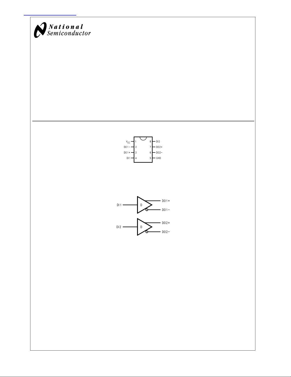
Connection Diagram
Order Number DS90C401M
See NS Package Number M08A
Functional Diagram
Features
n Ultra low power dissipation
n Operates above 155.5 Mbps
n Standard TIA/EIA-644
n 8 Lead SOIC Package saves space
n Low Differential Output Swing typical 340 mV
10001301
10001302
© 2005 National Semiconductor Corporation DS100013 www.national.com

Absolute Maximum Ratings (Note 1)
If Military/Aerospace specified devices are required,
please contact the National Semiconductor Sales Office/
DS90C401
Distributors for availability and specifications.
Supply Voltage (V
Input Voltage (D
Output Voltage (D
Short Circuit Duration
(D
OUT+,DOUT−
Maximum Package Power Dissipation
M Package 1068 mW
Derate M Package 8.5 mW/˚C above +25˚C
Storage Temperature Range −65˚C to +150˚C
) −0.3V to +6V
CC
) −0.3V to (VCC+ 0.3V)
IN
OUT+,DOUT−
) −0.3V to (VCC+ 0.3V)
) Continuous
@
+25˚C
Maximum Junction
Temperature +150˚C
ESD Rating
(HBM, 1.5 kΩ, 100 pF) ≥ 3,500V
(EIAJ, 0 Ω, 200 pF) ≥ 250V
Recommended Operating
Conditions
Min Typ Max Units
Supply Voltage (V
Operating Free Air
Temperature (T
) +4.5 +5.0 +5.5 V
CC
) −40 +25 +85 ˚C
A
Lead Temperature Range
Soldering (4 sec.) +260˚C
Electrical Characteristics
Over supply voltage and operating temperature ranges, unless otherwise specified. (Notes 2, 3)
Symbol Parameter Conditions Pin Min Typ Max Units
V
∆V
V
∆V
V
V
I
OS
V
V
I
I
V
I
CC
I
CCL
OD1
OD1
OS
OS
OH
OL
IH
IL
CL
Differential Output Voltage RL= 100Ω (Figure 1)D
Change in Magnitude of V
OD1
for
D
OUT−
OUT+
,
250 340 450 mV
4 35 |mV|
Complementary Output States
Offset Voltage 1.125 1.25 1.375 V
Change in Magnitude of VOSfor
5 25 |mV|
Complementary Output States
Output Voltage High RL= 100Ω 1.41 1.60 V
Output Voltage Low 0.90 1.07 V
Output Short Circuit Current V
Input Voltage High D
= 0V (Note 8) −3.5 −5.0 mA
OUT
2.0 V
IN
CC
Input Voltage Low GND 0.8 V
Input Current VIN=VCC, GND, 2.5V or 0.4V −10
±
1 +10 µA
Input Clamp Voltage ICL= −18 mA −1.5 −0.8 V
No Load Supply Current DIN=VCCor GND V
D
= 2.5V or 0.4V 3.5 5.5 mA
IN
Loaded Supply Current RL= 100Ω All Channels
V
IN=VCC
or GND (all inputs)
CC
1.7 3.0 mA
8 14.0 mA
V
Switching Characteristics
VCC= +5.0V±10%, TA= −40˚C to +85˚C (Notes 3, 4, 5, 6, 9)
Symbol Parameter Conditions Min Typ Max Units
t
PHLD
t
PLHD
t
SKD
t
SK1
t
SK2
t
TLH
t
THL
www.national.com 2
Differential Propagation Delay High to Low RL= 100Ω,CL=5pF
Differential Propagation Delay Low to High 0.5 2.1 3.5 ns
Differential Skew |t
PHLD–tPLHD
| 0 80 900 ps
(Figure 2 and Figure 3)
0.5 2.0 3.5 ns
Channel-to-Channel Skew (Note 4) 0 0.3 1.0 ns
Chip to Chip Skew (Note 5) 3.0 ns
Rise Time 0.35 2.0 ns
Fall Time 0.35 2.0 ns
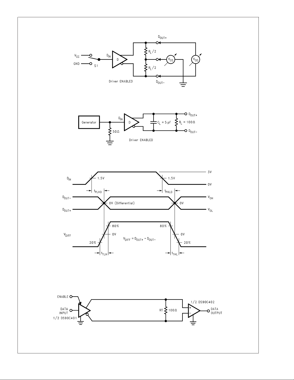
Parameter Measurement Information
FIGURE 1. Driver VODand VOSTest Circuit
DS90C401
10001304
10001305
FIGURE 2. Driver Propagation Delay and Transition Time Test Circuit
FIGURE 3. Driver Propagation Delay and Transition Time Waveforms
Typical Application
10001306
FIGURE 4. Point-to-Point Application
10001309
www.national.com3
Applications Information
LVDS drivers and receivers are intended to be primarily used
in an uncomplicated point-to-point configuration as is shown
DS90C401
in Figure 4. This configuration provides a clean signaling
environment for the quick edge rates of the drivers. The
receiver is connected to the driver through a balanced media
which may be a standard twisted pair cable, a parallel pair
cable, or simply PCB traces. Typically, the characteristic
impedance of the media is in the range of 100Ω. A termination resistor of 100Ω should be selected to match the media,
and is located as close to the receiver input pins as possible.
The termination resistor converts the current sourced by the
driver into a voltage that is detected by the receiver. Other
configurations are possible such as a multi-receiver configuration, but the effects of a mid-stream connector(s), cable
stub(s), and other impedance discontinuities as well as
ground shifting, noise margin limits, and total termination
loading must be taken into account.
The DS90C401 differential line driver is a balanced current
source design. A current mode driver, generally speaking
has a high output impedance and supplies a constant current for a range of loads (a voltage mode driver on the other
hand supplies a constant voltage for a range of loads).
Current is switched through the load in one direction to
produce a logic state and in the other direction to produce
the other logic state. The typical output current is mere 3.4
mA, a minimum of 2.5 mA, and a maximum of 4.5 mA. The
current mode requires (as discussed above) that a resistive
termination be employed to terminate the signal and to complete the loop as shown in Figure 4. AC or unterminated
configurations are not allowed. The 3.4 mA loop current will
develop a differential voltage of 340 mV across the 100Ω
termination resistor which the receiver detects with a 240 mV
minimum differential noise margin neglecting resistive line
losses (driven signal minus receiver threshold (340 mV –
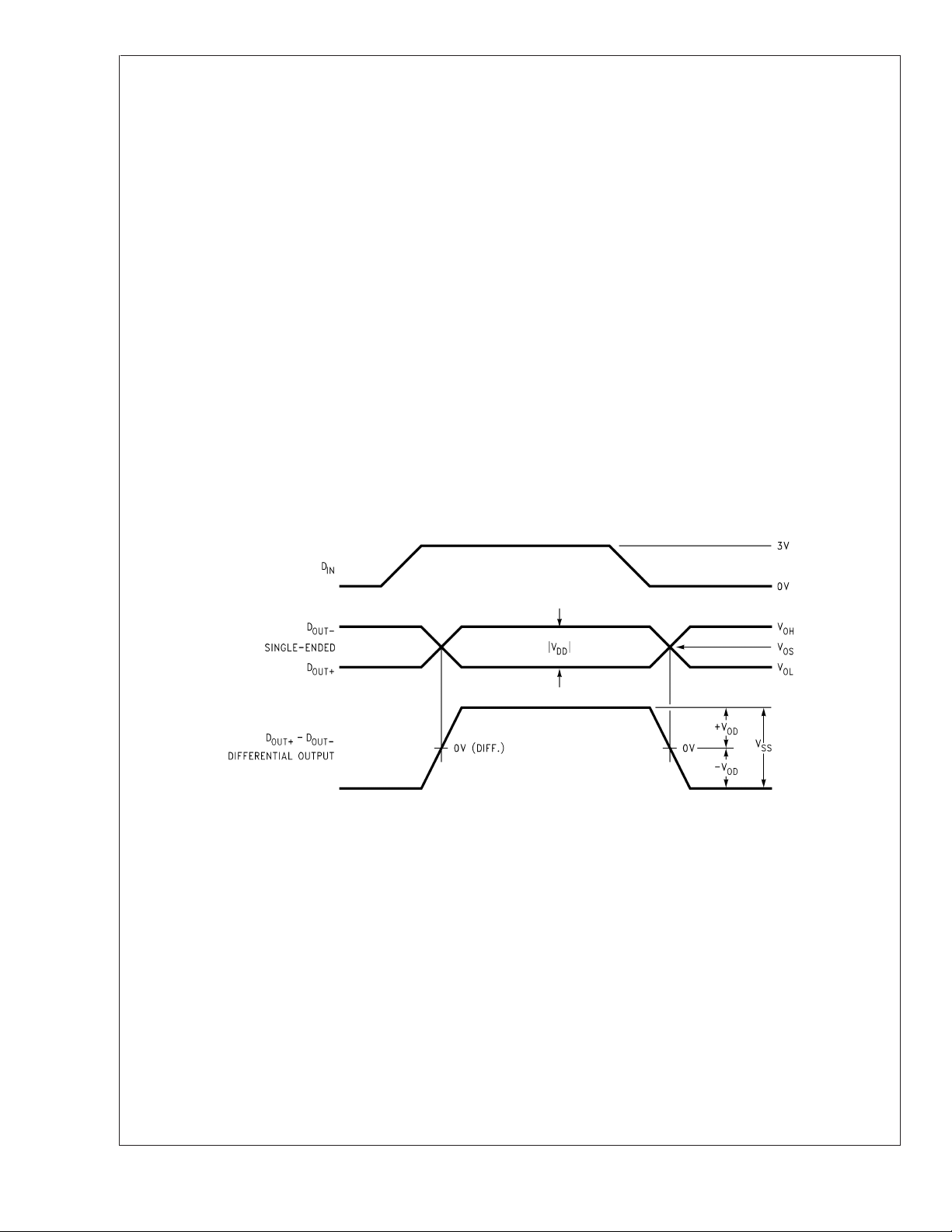
100 mV = 240 mV)). The signal is centered around +1.2V
(Driver Offset, V
Figure 5. Note that the steady-state voltage (V
peak swing is twice the differential voltage (V
) with respect to ground as shown in
OS
) peak-to-
SS
) and is
OD
typically 680 mV.
The current mode driver provides substantial benefits over
voltage mode drivers, such as an RS-422 driver. Its quiescent current remains relatively flat versus switching frequency. Whereas the RS-422 voltage mode driver increases
exponentially in most case between 20 MHz–50 MHz. This
is due to the overlap current that flows between the rails of
the device when the internal gates switch. Whereas the
current mode driver switches a fixed current between its
output without any substantial overlap current. This is similar
to some ECL and PECL devices, but without the heavy static
requirements of the ECL/PECL designs. LVDS requires
I
CC
>
80% less current than similar PECL devices. AC specifications for the driver are a tenfold improvement over other
existing RS-422 drivers.
FIGURE 5. Driver Output Levels
www.national.com 4
10001310
 Loading...