

查询DS90C385A供应商
PRELIMINARY
DS90C385A
+3.3V Programmable LVDS Transmitter 24-Bit Flat Panel
Display Link-87.5 MHz
DS90C385A +3.3V Programmable LVDS Transmitter 24-bit Flat Panel Display (FPD) Link-87.5 MHz
October 2005
General Description
The DS90C385A is a pin to pin compatible replacement for
DS90C383, DS90C383A and DS90C385. The DS90C385A
has additional features and improvements making it an ideal
replacement for DS90C383, DS90C383A and DS90C385.
family of LVDS Transmitters.
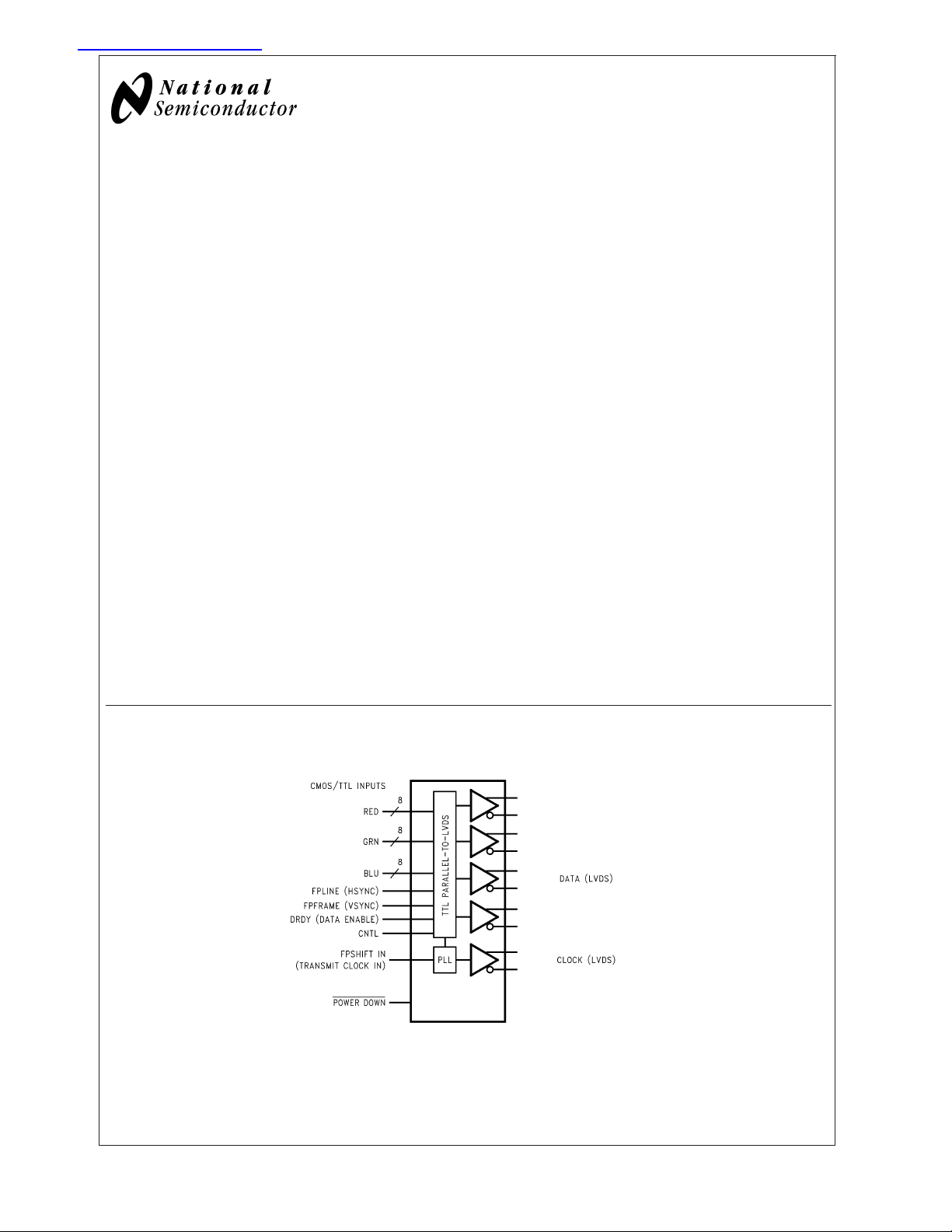
The DS90C385A transmitter converts 28 bits of LVCMOS/
LVTTL data into four LVDS (Low Voltage Differential Signaling) data streams. A phase-locked transmit clock is transmitted in parallel with the data streams over the fifth LVDS link.
Every cycle of the transmit clock 28 bits of input data are
sampled and transmitted. At a transmit clock frequency of
87.5 MHz, 24 bits of RGB data and 3 bits of LCD timing and
control data (FPLINE, FPFRAME, DRDY) are transmitted at
a rate of 612.5Mbps per LVDS data channel. Using a 87.5
MHz clock, the data throughput is 306.25Mbytes/sec. This
transmitter can be programmed for Rising edge strobe or
Falling edge strobe through a dedicated pin. A Rising edge
or Falling edge strobe transmitter will interoperate with a
Falling edge strobe FPDLink Receiver without any translation logic.
This chipset is an ideal means to solve EMI and cable size
problems associated with wide, high-speed TTL interfaces
with added Spread Spectrum Clocking support.
Features
n Pin-to-pin compatible to DS90C383, DS90C383A and
DS90C385 .
n No special start-up sequence required between
clock/data and /PD pins. Input signals (clock and data)
can be applied either before or after the device is
powered.
n Support Spread Spectrum Clocking up to 100kHz
frequency modulation & deviations of
spread or -5% down spread.
n “Input Clock Detection” feature will pull all LVDS pairs to
logic low when input clock is missing and when /PD pin
is logic high.
n 18 to 87.5 MHz shift clock support
n Tx power consumption
Grayscale
n Tx Power-down mode
n Supports VGA, SVGA, XGA, SXGA(dual pixel),
SXGA+(dual pixel), UXGA(dual pixel).
n Narrow bus reduces cable size and cost
n Up to 2.45 Gbps throughput
n Up to 306.25Megabytes/sec bandwidth
n 345 mV (typ) swing LVDS devices for low EMI
n PLL requires no external components
n Compliant to TIA/EIA-644 LVDS standard
n Low profile 56-lead TSSOP package
<
147 mW (typ)@87.5 MHz
<
60 µW (typ)
±
2.5% center
Block Diagram
DS90C385A
Order Number DS90C385AMT
See NS Package Number MTD56
© 2005 National Semiconductor Corporation DS200702 www.national.com
20070201
Absolute Maximum Ratings (Note 1)
If Military/Aerospace specified devices are required,
please contact the National Semiconductor Sales Office/
Distributors for availability and specifications.
DS90C385A
Supply Voltage (V
CMOS/TTL Input Voltage −0.5V to (V
LVDS Driver Output Voltage −0.3V to (V
LVDS Output Short Circuit
Duration Continuous
Junction Temperature +150˚C
Storage Temperature −65˚C to +150˚C
Lead Temperature
(Soldering, 4 sec) +260˚C
Maximum Package Power Dissipation Capacity
MTD56 (TSSOP)
Package:
DS90C385AMT 1.63 W
) −0.3V to +4V
CC
CC
CC
+ 0.3V)
+ 0.3V)
@
25˚C
Package Derating:
DS90C385AMT 12.5 mW/˚C above +25˚C
ESD Rating
(HBM, 1.5kΩ, 100pF) 7kV
(EIAJ, 0Ω, 200 pF) 500V
Latch Up Tolerance
@
25˚C
Recommended Operating
Conditions
Min Nom Max Units
Supply Voltage (V
Operating Free Air
Temperature (T
Supply Noise Voltage
)
(V
CC
TxCLKIN frequency 18 87.5 MHz
) 3.0 3.3 3.6 V
CC
) −10 +25 +70 ˚C
A
200 mV
Electrical Characteristics
Over recommended operating supply and temperature ranges unless otherwise specified.
Symbol Parameter Conditions Min Typ Max Units
LVCMOS/LVTTL DC SPECIFICATIONS
V
IH
V
IL
V
CL
I
IN
LVDS DC SPECIFICATIONS
V
OD
∆V
OD
V
OS
∆V
OS
I
OS
I
OZ
TRANSMITTER SUPPLY CURRENT
ICCTW Transmitter Supply Current
High Level Input Voltage 2.0 V
CC
Low Level Input Voltage 0 0.8 V
Input Clamp Voltage ICL= −18 mA −0.79 −1.5 V
Input Current VIN= 0.4V, 2.5V or V
V
= GND −10 0 µA
IN
CC
+1.8 +10 µA
Differential Output Voltage RL= 100Ω 250 345 450 mV
Change in VODbetween
35 mV
complimentary output states
Offset Voltage (Note 4) 1.13 1.25 1.38 V
Change in VOSbetween
35 mV
complimentary output states
Output Short Circuit Current V
Output TRI-STATE®Current Power Down = 0V,
Worst Case
= 0V, RL= 100Ω −3.5 −5 mA
OUT
±
1
V
=0VorV
OUT
R
= 100Ω,
L
= 5 pF,
C
L
Worst Case Pattern
CC
f = 25 MHz 31 45 mA
f = 40 MHz 37 50 mA
±
10 µA
(Figures 1, 3 ) ” Typ ”
values are given for
= 3.6V and TA=
V
CC
f = 65 MHz 48 60 mA
+25˚C, ” Max ” values
are given for V
3.6V and T
A
=
CC
= −10˚C
f = 87.5 MHz 55 65 mA
±
100mA
PP
V
www.national.com 2
Electrical Characteristics (Continued)
Over recommended operating supply and temperature ranges unless otherwise specified.
Symbol Parameter Conditions Min Typ Max Units
TRANSMITTER SUPPLY CURRENT
ICCTG Transmitter Supply Current
16 Grayscale
R
L
C
L
= 100Ω,
= 5 pF,
16 Grayscale Pattern
(Figures 2, 3 ) ” Typ ”
values are given for
= 3.6V and TA=
V
CC
+25˚C, ” Max ” values
CC
= −10˚C
A
=
ICCTZ Transmitter Supply Current
Power Down
are given for V
3.6V and T
Power Down = Low
Driver Outputs in TRI-STATE under
Power Down Mode
Note 1: “Absolute Maximum Ratings” are those values beyond which the safety of the device cannot be guaranteed. They are not meant to imply that the device
should be operated at these limits. The tables of “Electrical Characteristics” specify conditions for device operation.
Note 2: Typical values are given for V
Note 3: Current into device pins is defined as positive. Current out of device pins is defined as negative. Voltages are referenced to ground unless otherwise
specified (except V
Note 4: V
OS
and ∆VOD).
OD
previously referred as VCM.
= 3.3V and TA= +25C unless specified otherwise.
CC
f = 25 MHz 29 40 mA
f = 40 MHz 33 45 mA
f = 65 MHz 39 50 mA
f = 87.5 MHz 44 55 mA
17 150 µA
DS90C385A
Recommended Transmitter Input Characteristics
Over recommended operating supply and temperature ranges unless otherwise specified
Symbol Parameter Min Typ Max Units
TCIT TxCLK IN Transition Time (Figure 5) 1.0 6.0 ns
TCIP TxCLK IN Period (Figure 6) 11.42 T 55.55 ns
TCIH TxCLK IN High Time (Figure 6) 0.35T 0.5T 0.65T ns
TCIL TxCLK IN Low Time (Figure 6) 0.35T 0.5T 0.65T ns
TXIT TxIN , and PWR DOWN pin Transition Time
TXPD Minimum pulse width for PWR DOWN pin signal.
1.5 6.0 ns
1us
Transmitter Switching Characteristics
Over recommended operating supply and temperature ranges unless otherwise specified
Symbol Parameter Min Typ Max Units
LLHT LVDS Low-to-High Transition Time (Figure 4) 0.75 1.4 ns
LHLT LVDS High-to-Low Transition Time (Figure 4) 0.75 1.4 ns
TPPos0 Transmitter Output Pulse Position (Figure 12)
(Note 5)
TPPos1 Transmitter Output Pulse Position 5.26 5.71 6.16 ns
TPPos2 Transmitter Output Pulse Position 10.98 11.43 11.88 ns
TPPos3 Transmitter Output Pulse Position 16.69 17.14 17.59 ns
TPPos4 Transmitter Output Pulse Position 22.41 22.86 23.31 ns
TPPos5 Transmitter Output Pulse Position 28.12 28.57 29.02 ns
TPPos6 Transmitter Output Pulse Position 33.84 34.29 34.74 ns
f = 25MHz −0.45 0 +0.45 ns
www.national.com3
Transmitter Switching Characteristics (Continued)
Over recommended operating supply and temperature ranges unless otherwise specified
Symbol Parameter Min Typ Max Units
DS90C385A
TPPos0 Transmitter Output Pulse Position (Figure 12)
(Note 5)
TPPos1 Transmitter Output Pulse Position 3.32 3.57 3.82 ns
TPPos2 Transmitter Output Pulse Position 6.89 7.14 7.39 ns
TPPos3 Transmitter Output Pulse Position 10.46 10.71 10.96 ns
TPPos4 Transmitter Output Pulse Position 14.04 14.29 14.54 ns
TPPos5 Transmitter Output Pulse Position 17.61 17.86 18.11 ns
TPPos6 Transmitter Output Pulse Position 21.18 21.43 21.68 ns
TPPos0 Transmitter Output Pulse Position (Figure 12)
(Note 5)
TPPos1 Transmitter Output Pulse Position 2.00 2.20 2.40 ns
TPPos2 Transmitter Output Pulse Position for Bit 2 4.20 4.40 4.60 ns
TPPos3 Transmitter Output Pulse Position for Bit 3 6.39 6.59 6.79 ns
TPPos4 Transmitter Output Pulse Position 8.59 8.79 8.99 ns
TPPos5 Transmitter Output Pulse Position 10.79 10.99 11.19 ns
TPPos6 Transmitter Output Pulse Position 12.99 13.19 13.39 ns
TPPos0 Transmitter Output Pulse Position (Figure 12)
(Note 5)
TPPos1 Transmitter Output Pulse Position 1.48 1.68 1.88 ns
TPPos2 Transmitter Output Pulse Position 3.16 3.36 3.56 ns
TPPos3 Transmitter Output Pulse Position 4.84 5.04 5.24 ns
TPPos4 Transmitter Output Pulse Position 6.52 6.72 6.92 ns
TPPos5 Transmitter Output Pulse Position 8.20 8.40 8.60 ns
TPPos6 Transmitter Output Pulse Position 9.88 10.08 10.28 ns
TSTC Required TxIN Setup to TxCLK IN
(Figure 6) at 85MHz
THTC Required TxIN Hold to TxCLK IN (Figure 6) at
87.5 MHz
TCCD TxCLK IN to TxCLK OUT Delay. Measure from
TxCLK IN edge to immediately crossing point of
differential TxCLK OUT by following the positive
TxCLK OUT. 50% duty cycle input clock is
assumed. (Figure 7)
Measure from TxCLK IN edge to immediately
crossing point of differential TxCLK OUT by
following the positive TxCLK OUT. 50% duty
cycle input clock is assumed. (Figure 8)
f = 40 MHz −0.25 0 +0.25 ns
f = 65 MHz −0.20 0 +0.20 ns
f = 87.5 MHz −0.20 0 +0.20 ns
2.5 ns
0.5 ns
T
= −10˚,
A
3.086 7.211 ns
and 87.5MHz
for " Min ",
= 70˚, and
T
A
25MHz for "
Max ", V
=
CC
3.6V, R_FB
pin = VCC
T
A
= −10˚,
2.868 6.062 ns
and 87.5MHz
for " Min ",
= 70˚, and
T
A
25MHz for "
Max ", V
=
CC
3.6V, R_FB
pin = GND
www.national.com 4
 Loading...