

查询DS90C363B供应商
PRELIMINARY
DS90C363B
+3.3V Programmable LVDS Transmitter 18-Bit Flat Panel
Display (FPD) Link -65 MHz
DS90C363B +3.3V Programmable LVDS Transmitter 18-Bit Flat Panel Display (FPD) Link -65 MHz
August 2005
General Description
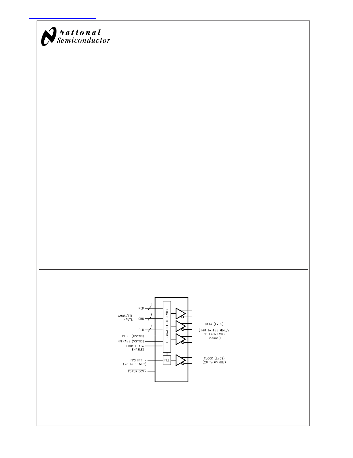
The DS90C363B transmitter converts 21 bits of CMOS/TTL
data into three LVDS (Low Voltage Differential Signaling)
data streams. A phase-locked transmit clock is transmitted in
parallel with the data streams over a fourth LVDS link. Every
cycle of the transmit clock 21 bits of input data are sampled
and transmitted. At a transmit clock frequency of 65 MHz, 18
bits of RGB data and 3 bits of LCD timing and control data
(FPLINE, FPFRAME, DRDY) are transmitted at a rate of 455
Mbps per LVDS data channel. Using a 65 MHz clock, the
data throughput is 170 Mbytes/sec. The DS90C363B transmitter can be programmed for Rising edge strobe or Falling
edge strobe through a dedicated pin. A Rising edge or
Falling edge strobe transmitter will interoperate with a Falling
edge strobe Receiver (DS90CF366) without any translation
logic.
This chipset is an ideal means to solve EMI and cable size
problems associated with wide, high speed TTL interfaces.
Features
n No special start-up sequence required between
clock/data and /PD pins. Input signal (clock and data)
can be applied either before or after the device is
powered.
n Support Spread Spectrum Clocking up to 100kHz
frequency modulation & deviations of
spread or −5% down spread.
n "Input Clock Detection" feature will pull all LVDS pairs to
logic low when input clock is missing and when /PD pin
is logic high.
n 18 to 68 MHz shift clock support
n Best–in–Class Set & Hold Times on TxINPUTs
n Tx power consumption
Grayscale
n 40% Less Power Dissipation than BiCMOS Alternatives
n Tx Power-down mode
n Supports VGA, SVGA, XGA and Dual Pixel SXGA.
n Narrow bus reduces cable size and cost
n Up to 1.3 Gbps throughput
n Up to 170 Megabytes/sec bandwidth
n 345 mV (typ) swing LVDS devices for low EMI
n PLL requires no external components
n Compatible with TIA/EIA-644 LVDS standard
n Low profile 48-lead TSSOP package
n Improved replacement for:
SN75LVDS84, DS90C363A
<
130 mW (typ)@65MHz
<
37µW (typ)
±
2.5% center
Block Diagram
DS90C363B
Order Number DS90C363BMT
See NS Package Number MTD48
TRI-STATE®is a registered trademark of National Semiconductor Corporation.
© 2005 National Semiconductor Corporation DS200986 www.national.com
20098601
Absolute Maximum Ratings (Note 1)
If Military/Aerospace specified devices are required,
please contact the National Semiconductor Sales Office/
Distributors for availability and specifications.
DS90C363B
Supply Voltage (V
CMOS/TTL Input Voltage −0.3V to (V
LVDS Driver Output Voltage −0.3V to (V
LVDS Output Short Circuit
Duration Continuous
Junction Temperature +150˚C
Storage Temperature −65˚C to +150˚C
Lead Temperature
(Soldering, 4 sec) +260˚C
Maximum Package Power Dissipation Capacity
MTD48 (TSSOP) Package:
DS90C363B 1.98 W
) −0.3V to +4V
CC
CC
CC
@
+ 0.3V)
+ 0.3V)
25˚C
Package Derating:
DS90C363B 16 mW/˚C above +25˚C
ESD Rating
(HBM, 1.5 kΩ, 100 pF) 7 kV
(EIAJ, 0Ω, 200 pF) 500V
Recommended Operating
Conditions
Min Nom Max Units
Supply Voltage (V
Operating Free Air
Temperature (T
Supply Noise Voltage
(VCC)
TxCLKIN frequency 18 68 MHz
) 3.0 3.3 3.6 V
CC
) −10 +25 +70 ˚C
A
200 mV
Electrical Characteristics
Over recommended operating supply and temperature ranges unless otherwise specified.
Symbol Parameter Conditions Min Typ Max Units
CMOS/TTL DC SPECIFICATIONS
V
IH
V
IL
V
CL
I
IN
LVDS DC SPECIFICATIONS
V
OD
∆V
OD
V
OS
∆V
OS
I
OS
I
OZ
TRANSMITTER SUPPLY CURRENT
ICCTW Transmitter Supply Current
High Level Input Voltage 2.0 V
CC
Low Level Input Voltage GND 0.8 V
Input Clamp Voltage ICL= −18 mA −0.79 −1.5 V
Input Current VIN= 0.4V, 2.5V or V
V
= GND −10 0 µA
IN
CC
+1.8 +10 µA
Differential Output Voltage RL= 100Ω 250 345 450 mV
Change in VODbetween
35 mV
complimentary output states
Offset Voltage (Note 4) 1.13 1.25 1.38 V
Change in VOSbetween
35 mV
complimentary output states
Output Short Circuit Current V
Output TRI-STATE®Current Power Down = 0V,
Worst Case
= 0V, RL= 100Ω −3.5 −5 mA
OUT
±
1
V
=0VorV
OUT
R
L
C
L
= 100Ω,
= 5 pF,
CC
f = 25MHz 29 40 mA
±
10 µA
Worst Case Pattern
(Figures 1, 4 ) " Typ "
f = 40 MHz 34 45 mA
values are given for V
CC
= 3.6V and TA=
+25˚C, " Max " values
are given for V
3.6V and T
CC
= −10˚C
A
f = 65 MHz 42 55 mA
=
PP
V
www.national.com 2
Electrical Characteristics (Continued)
Over recommended operating supply and temperature ranges unless otherwise specified.
Symbol Parameter Conditions Min Typ Max Units
TRANSMITTER SUPPLY CURRENT
ICCTG Transmitter Supply Current
16 Grayscale
R
L
C
L
= 100Ω,
= 5 pF,
16 Grayscale Pattern
(Figures 2, 4 ) " Typ "
values are given for V
CC
= 3.6V and TA=
+25˚C, " Max " values
ICCTZ Transmitter Supply Current
Power Down
are given for V
3.6V and T
Power Down = Low
Driver Outputs in TRI-STATE®under
CC
= −10˚C
A
Power Down Mode
Note 1: “Absolute Maximum Ratings” are those values beyond which the safety of the device cannot be guaranteed. They are not meant to imply that the device
should be operated at these limits. The tables of “Electrical Characteristics” specify conditions for device operation.
Note 2: Typical values are given for V
Note 3: Current into device pins is defined as positive. Current out of device pins is defined as negative. Voltages are referenced to ground unless otherwise
specified (except V
Note 4: V
OS
and ∆VOD).
OD
previously referred as VCM.
= 3.3V and TA= +25˚C unless specified otherwise.
CC
f = 25 MHz 28 40 mA
f = 40 MHz 32 45 mA
f = 65 MHz 39 50 mA
=
11 150 µA
DS90C363B
Recommended Transmitter Input Characteristics
Over recommended operating supply and temperature ranges unless otherwise specified
Symbol Parameter Min Typ Max Units
TCIT TxCLK IN Transition Time (Figure 5 ) 5ns
TCIP TxCLK IN Period (Figure 6 ) 14.7 T 50 ns
TCIH TxCLK IN High Time (Figure 6 ) 0.35T 0.5T 0.65T ns
TCIL TxCLK IN Low Time (Figure 6 ) 0.35T 0.5T 0.65T ns
TXIT TxIN, and Power Down pin transition Time
TXPD Minimum pulse width for Power Down pin signal
1.5 6.0 ns
1us
Transmitter Switching Characteristics
Over recommended operating supply and temperature ranges unless otherwise specified
Symbol Parameter Min Typ Max Units
LLHT LVDS Low-to-High Transition Time (Figure 4 ) 0.75 1.4 ns
LHLT LVDS High-to-Low Transition Time (Figure 4 ) 0.75 1.4 ns
TPPos0 Transmitter Output Pulse Position for Bit 0 (Figure 11 ) (Note 5) f = 65
TPPos1 Transmitter Output Pulse Position for Bit 1 2.00 2.20 2.40 ns
MHz
TPPos2 Transmitter Output Pulse Position for Bit 2 4.20 4.40 4.60 ns
TPPos3 Transmitter Output Pulse Position for Bit 3 6.39 6.59 6.79 ns
TPPos4 Transmitter Output Pulse Position for Bit 4 8.59 8.79 8.99 ns
TPPos5 Transmitter Output Pulse Position for Bit 5 10.79 10.99 11.19 ns
TPPos6 Transmitter Output Pulse Position for Bit 6 12.99 13.19 13.39 ns
TPPos0 Transmitter Output Pulse Position for Bit 0 (Figure 11 ) (Note 5) f = 40
TPPos1 Transmitter Output Pulse Position for Bit 1 3.32 3.57 3.82 ns
MHz
TPPos2 Transmitter Output Pulse Position for Bit 2 6.89 7.14 7.39 ns
TPPos3 Transmitter Output Pulse Position for Bit 3 10.46 10.71 10.96 ns
TPPos4 Transmitter Output Pulse Position for Bit 4 14.04 14.29 14.54 ns
TPPos5 Transmitter Output Pulse Position for Bit 5 17.61 17.86 18.11 ns
TPPos6 Transmitter Output Pulse Position for Bit 6 21.18 21.43 21.68 ns
−0.20 0 0.20 ns
−0.25 0 0.25 ns
www.national.com3
Transmitter Switching Characteristics (Continued)
Over recommended operating supply and temperature ranges unless otherwise specified
Symbol Parameter Min Typ Max Units
DS90C363B
TPPos0 Transmitter Output Pulse Position for Bit 0 (Figure 11 ) (Note 5) f = 25
TPPos1 Transmitter Output Pulse Position for Bit 1 5.26 5.71 6.16 ns
MHz
TPPos2 Transmitter Output Pulse Position for Bit 2 10.98 11.43 11.83 ns
TPPos3 Transmitter Output Pulse Position for Bit 3 16.69 17.14 17.54 ns
TPPos4 Transmitter Output Pulse Position for Bit 4 22.41 22.86 23.26 ns
TPPos5 Transmitter Output Pulse Position for Bit 5 28.12 28.57 28.97 ns
TPPos6 Transmitter Output Pulse Position for Bit 6 33.84 34.29 34.69 ns
TSTC TxIN Setup to TxCLK IN (Figure 6 ) 2.5 ns
THTC TxIN Hold to TxCLK IN (Figure 6 ) 0.5 ns
TCCD TxCLK IN to TxCLK OUT Delay (Figure 7 ) 50% duty cycle input
clock is assumed, T
and 25MHz for ” Max ”, V
= −10˚C, and 65MHz for ” Min ”, TA= 70˚C,
A
= 3.6V, R_FB = V
CC
CC
TxCLK IN to TxCLK OUT Delay (Figure 7 ) 50% duty cycle input
clock is assumed, T
and 25MHz for ” Max ”, V
SSCG Spread Spectrum Clock support; Modulation frequency with a
linear profile (Note 6)
= −10˚C, and 65MHz for ” Min ”, TA= 70˚C,
A
= 3.6V, R_FB = GND
CC
f=25
MHz
f=40
MHz
f=65
MHz
TPLLS Transmitter Phase Lock Loop Set (Figure 8 ) 10 ms
TPDD Transmitter Power Down Delay (Figure 10 ) 100 ns
Note 5: The Minimum and Maximum Limits are based on statistical analysis of the device performance over process, voltage, and temperature ranges. This
parameter is functionality tested only on Automatic Test Equipment (ATE).
Note 6: Care must be taken to ensure TSTC and THTC are met so input data are sampling correctly. This SSCG parameter only shows the performance of tracking
Spread Spectrum Clock applied to TxCLK IN pin, and reflects the result on TxCLKOUT+ and TxCLK− pins.
−0.450 0 +0.450 ns
3.340 7.211 ns
3.011 6.062 ns
100kHz
±
2.5%/−5%
100kHz
±
2.5%/−5%
100kHz
±
2.5%/−5%
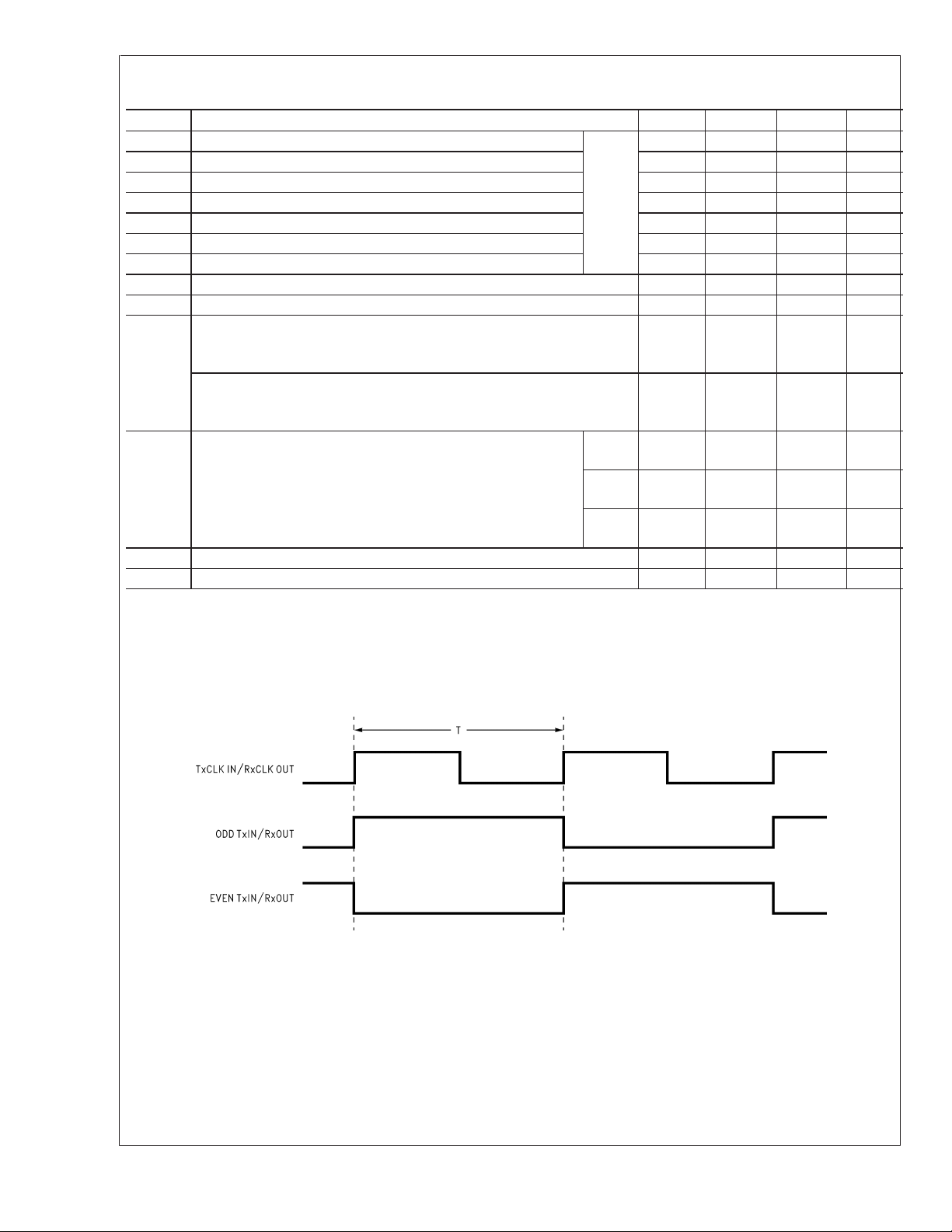
AC Timing Diagrams
20098604
FIGURE 1. “Worst Case” Test Pattern
www.national.com 4
 Loading...