

DS90C3202
3.3V 8 MHz to 135 MHz Dual FPD-Link Receiver
DS90C3202 3.3V 8 MHz to 135 MHz Dual FPD-Link Receiver
September 2006
General Description
The DS90C3202 is a 3.3V single/dual FPD-Link 10-bit color
receiver is designed to be used in Liquid Crystal Display
TVs, LCD Monitors, Digital TVs, and Plasma Display Panel
TVs. The DS90C3202 is designed to interface between the
digital video processor and the display device using the
low-power, low-EMI LVDS (Low Voltage Differential Signaling) interface. The DS90C3202 converts up to ten LVDS
data streams back into 70 bits of parallel LVCMOS/LVTTL
data. The receiver can be programmed with rising edge or
falling edge clock. Optional wo-wire serial programming allows fine tuning in development and production environments. With an input clock at 135 MHz, the maximum transmission rate of each LVDS line is 945 Mbps, for an
aggregate throughput rate of 9.45 Gbps (945 Mbytes/s). This
allows the dual 10-bit LVDS Receiver to support resolutions
up to HDTV.
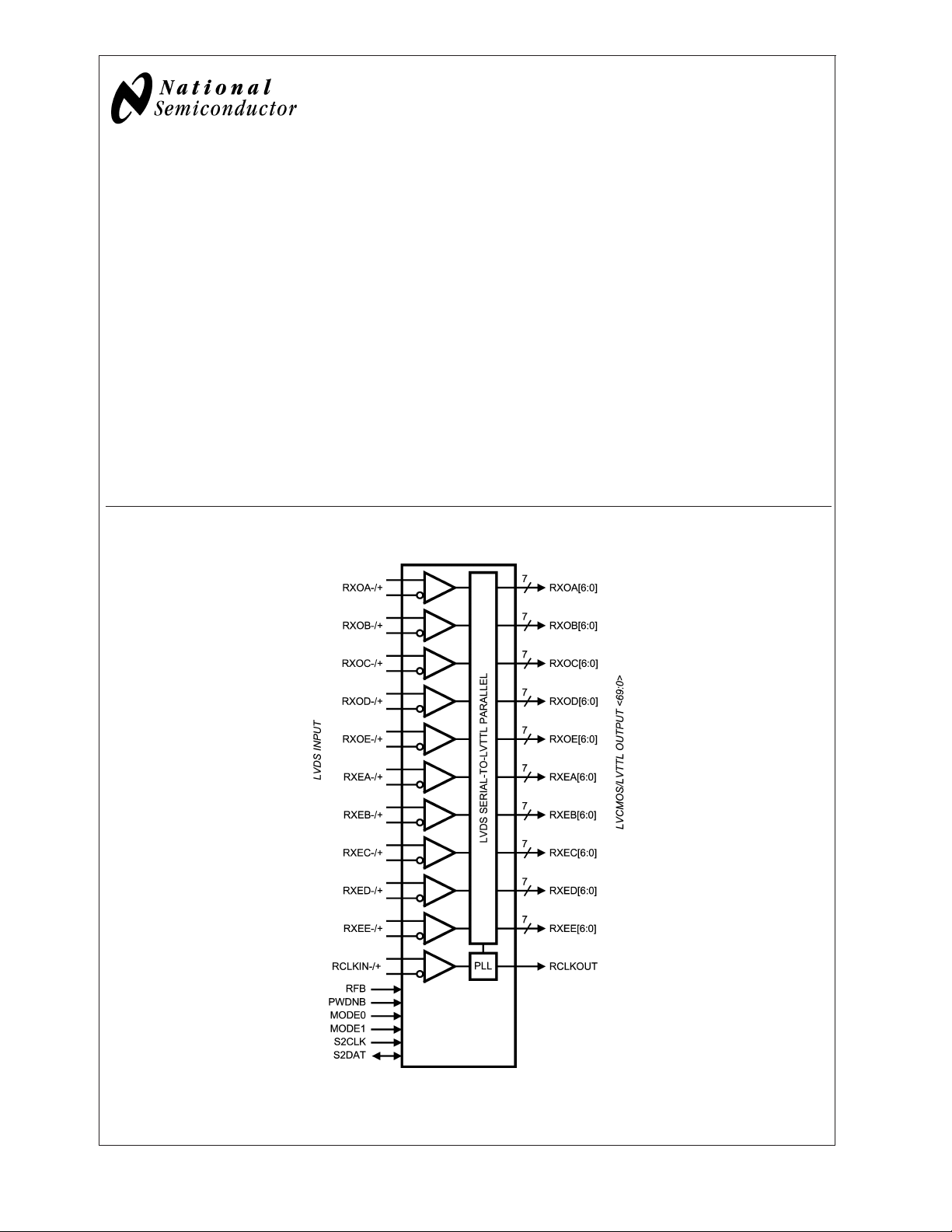
Block Diagram
Features
n Up to 9.45 Gbit/s data throughput
n 8 MHz to 135 MHz input clock support
n Supports up to QXGA panel resolutions
n Supports HDTV panel resolutions and frame rates up to
1920 x 1080p
n LVDS 30-bit, 24-bit or 18-bit color data inputs
n Supports single pixel and dual pixel interfaces
n Supports spread spectrum clocking
n Two-wire serial communication interface
n Programmable clock edge and control strobe select
n Power down mode
n +3.3V supply voltage
n 128-pin TQFP Package
n Compliant to TIA/EIA-644-A-2001 LVDS Standard
FIGURE 1. Receiver Block Diagram
© 2006 National Semiconductor Corporation DS201471 www.national.com
20147101
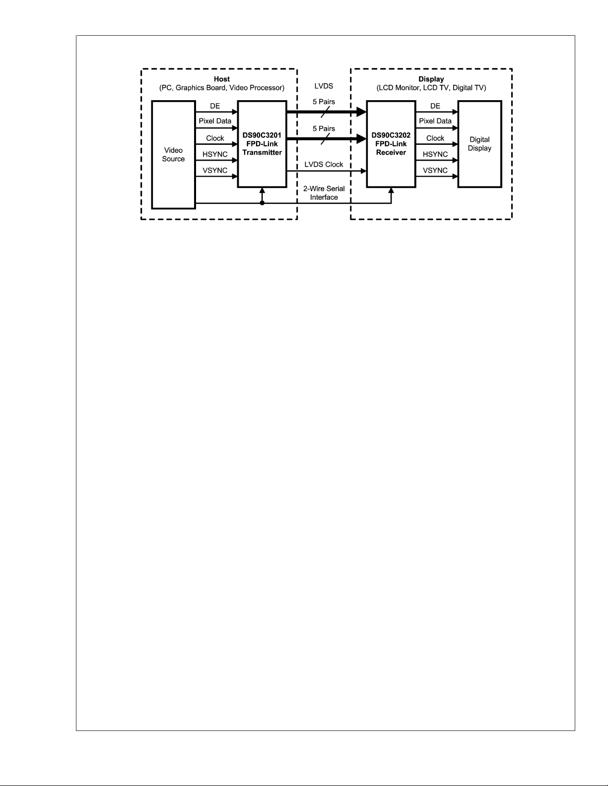
Typical Application Diagram
DS90C3202
FIGURE 2. LCD Panel Application Diagram
Functional Description
The DS90C3201 and DS90C3202 are a dual 10-bit color
Transmitter and Receiver FPD-Link chipset designed to
transmit data at clocks speeds from 8 to 135 MHz.
DS90C3201 and DS90C3202 are designed to interface between the digital video processor and the display using a
LVDS interface. The DS90C3201 transmitter serializes 2
channels of video data (10-bit each for RGB for each channel, totaling 60 bits) and control signals (HSYNC, VSYNC,
DE and two user-defined signals) along with clock signal to
10 channels of LVDS signals and transmits them. The
DS90C3202 receiver converts 10 channels of LVDS signals
into parallel signals and outputs 2 channels of video data
(10-bit each for RGB for each channel, totaling 60 bits) and
control signals (HSYNC, VSYNC, DE and two user-defined
signals) along with clock signal. The dual high speed LVDS
channels supports single pixel in-single pixel out and dual
pixel in-dual pixel out transmission modes. The FPD-Link
chipset is suitable for a variety of display applications including LCD Monitors, LCD TV, Digital TV, and DLP TV, and
Plasma Display Panels.
Using a true 10-bit color depth system, the 30-bit RGB color
produces over 1.07 billion colors to represent High Definition
(HD) displays in their most natural color, surpassing the
maximum 16.7 million colors achieved by 6/8-bit color conventionally used for large-scale LCD televisions and LCD
monitors.
LVDS RECEIVER
The LVDS Receiver receives input RGB video data and
control signal timing.
20147102
2-WIRE SERIAL COMMUNICATION INTERFACE
Optional Two-Wire serial interface programming allows fine
tuning in development and production environments. The
Two-Wire serial interface provides several capabilities to
reduce EMI and to customize output timing. These capabilities are selectable/programmable via Two-Wire serial interface: Programmable Skew Rates, Progress Turn On Function, Input/Output Channel Control.
PROGRAMMABLE SKEW RATES
Programmable edge rates allow the LVCMOS/LVTTL Data
and Clock outputs to be adjusted for better impedance
matching for noise and EMI reduction. The individual output
drive control registers for Rx data out and Rx clock out are
programmable via Two-Wire serial interface.
PROGRESS TURN ON FUNCTION
Progress Turn On (PTO) function aligns the two output channels of LVCMOS/LVTLL in either a non-skew data format
(simultaneous switching) or a skewed data format (staggered). The skewed format delays the selected channel data
and staggers the outputs. This reduces the number of outputs switching simultaneously, which lowers EMI radiation
and minimizes ground bounce. Feature is controlled via
Two-Wire serial interface.
INPUT/OUTPUT CHANNEL CONTROL
Full independent control for input/output channels can be
disabled to minimize power supply line noise and overall
power dissipation. Feature is configured via Two-Wire serial
interface
SELECTABLE OUTPUT DATA STROBE
The Receiver output data edge strobe can be latched on the
rising or falling edges of clock signal. The dedicated RFB pin
is used to program output strobe select on the rising edge of
RCLK or the falling edge of RCLK.
www.national.com 2
DS90C3202
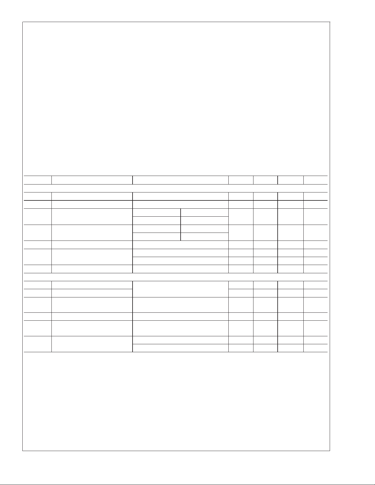
Absolute Maximum Ratings (Note 1)
If Military/Aerospace specified devices are required,
please contact the National Semiconductor Sales Office/
Distributors for availability and specifications.
Supply Voltage (V
LVCMOS/LVTTL Input
Voltage −0.3V to (V
LVCMOS/LVTTL Output
Voltage −0.3V to (VDD+ 0.3V)
LVDS Receiver Input Voltage −0.3V to (V
Junction Temperature +150˚C
Storage Temperature −65˚C to +150˚C
Lead Temperature
(Soldering, 10 sec.) +260˚C
Maximum Package Power Dissipation Capacity
) −0.3V to +4V
DD
+ 0.3V)
DD
+ 0.3V)
DD
@
25˚C
Package Derating: 25.6mW/˚C above +25˚C
ESD Rating:
(HBM, 1.5kΩ, 100pF)
(EIAJ, 0Ω, 200pF)
>
>
2kV
200 V
Recommended Operating Conditions
Min Nom Max Units
Supply Voltage (V
Operating Free Air
Temperature (TA) 0 +25 +70 ˚C
Supply Noise Voltage (V
Receiver Input Range 0 V
Input Clock Frequency (f) 8 135 MHz
) 3.15 3.3 3.6 V
DD
P-P
)
±
100 mV
DD
p-p
V
128 TQFP Package: 1.4W
Electrical Characteristics
Over recommended operating supply and temperature ranges unless otherwise specified.
Symbol Parameter Conditions Min Typ Max Units
CMOS/TTL DC SPECIFICATIONS (Rx outputs, control inputs and outputs)
V
IH
V
IL
V
OH
V
OL
V
CL
I
IN
I
OS
LVDS RECEIVER DC SPECIFICATIONS
V
TH
V
TL
V
IN
| Differential Input Voltage 0.200 0.600 V
|V
ID
V
CM
I
IN
High Level Input Voltage 2.0 V
DD
Low Level Input Voltage 0 0.8 V
High Level Output Voltage Rx clock out IOH=−4mA 2.4 V
Rx data out I
=−2mA
OH
Low Level Output Voltage Rx clock out IOL=+4mA 0.4 V
Rx data out I
=+2mA
OL
Input Clamp Voltage ICL= −18 mA −0.8 −1.5 V
Input Current VIN=V
V
= 0V −10 µA
IN
Output Short Circuit Current V
= 0V −120 mA
OUT
DD
+10 µA
Differential Input High Threshold VCM= +1.2V +100 mV
Differential Input Low Threshold −100 mV
Input Voltage Range
0V
DD
(Single-ended)
Differential Common Mode
0.2 1.2 VDD−0.1 V
Voltage
Input Current VIN= +2.4V, VDD= 3.6V
V
= 0V, VDD= 3.6V
IN
±
10 µA
±
10 µA
V
V
www.national.com3
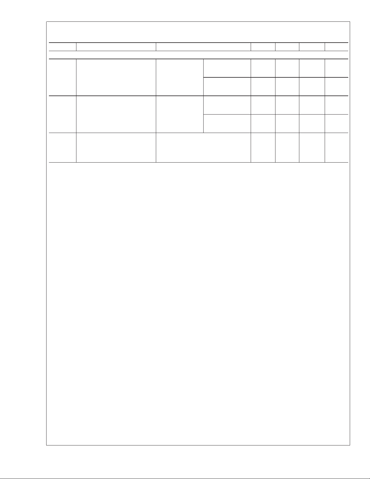
Electrical Characteristics (Continued)
Over recommended operating supply and temperature ranges unless otherwise specified.
Symbol Parameter Conditions Min Typ Max Units
DS90C3202
RECEIVER SUPPLY CURRENT
ICCRW Receiver Supply Current
Worst Case
(Figures 2, 4)
ICCRG Receiver Supply Current
Incremental Test Pattern
(Figures 3, 4)
ICCRZ Receiver Supply Current
Power Down
Note 1: “Absolute Maximum Ratings” are those values beyond which the safety of the device cannot be guaranteed. They are not meant to imply that the device
should be operated at these limits. The tables of “Electrical Characteristics” specify conditions for device operation.
Note 2: Typical values are given for V
Note 3: Current into device pins is defined as positive. Current out of device pins is defined as negative. Voltages are referenced to ground unless otherwise
specified.
Note 4: The worst case test pattern produces a maximum toggling of digital circuits, LVDS I/O and LVCMOS/LVTTL I/O.
Note 5: The incremental test pattern tests device power consumption for a “typical” LCD display pattern.
Note 6: Figures 2, 3 show a falling edge data strobe (RCLK OUT).
Note 7: Figure 8 show a rising edge data strobe (RCLK OUT).
= 3.3V and TA= +25˚C.
DD
= 8 pF,
C
L
f = 8 MHz 65 130 mA
Worst Case
Pattern
Default Register
f = 135 MHz 375 550 mA
Settings
C
L
= 8 pF,
f = 8 MHz 55 120 mA
Worst Case
Pattern
Default Register
f = 135 MHz 245 400 mA
Settings
PDWNB = Low
Receiver Outputs stay low
during Powerdown mode.
Default Register Settings
2mA
www.national.com 4
DS90C3202
Receiver Switching Characteristics
Over recommended operating supply and temperature ranges unless otherwise specified.
Symbol Parameter Condition/
Reference
CLHT LVCMOS/LVTTL Low-to-High Transition
Time, C
= 8pF, (Figure 5) (Note 8)
L
Rx clock out 1.45 2.10 ns
Register addr 28d/1ch,
bit [2] (RCLK)=0b (Default),
Rx data out 2.40 3.50 ns
bit [1] (RXE) =0b (Default),
bit [0] (RXO) =0b (Default)
CHLT LVCMOS/LVTTL High-to-Low Transition
Time, C
= 8pF, (Figure 5) (Note 8)
L
Rx clock out 1.35 2.20 ns
Register addr 28d/1ch,
bit [2] (RCLK)=0b (Default),
Rx data out 2.40 3.60 ns
bit [1] (RXE) =0b (Default),
bit [0] (RXO) =0b (Default)
CLHT
Programmable
adjustment
LVCMOS/LVTTL Low-to-High Transition
Time, C
= 8pF, (Figure 5) (Note 8)
L
Register addr 28d/1ch,
bit [2] (RCLK)=1b (Default),
Rx clock out 2.45 ns
Rx data out 3.40 ns
bit [1] (RXE) =1b (Default),
bit [0] (RXO) =1b (Default)
CHLT
Programmable
adjustment
LVCMOS/LVTTL High-to-Low Transition
Time, C
= 8pF, (Figure 5) (Note 8)
L
Register addr 28d/1ch,
bit [2] (RCLK)=0b (Default),
Rx clock out 2.35 ns
Rx data out 3.40 ns
bit [1] (RXE) =0b (Default),
bit [0] (RXO) =0b (Default)
RCOP RCLK OUT Period (Figures 11, 12) (Note 8) 8–135 MHz 7.4 T 125 ns
RCOH RCLK OUT High Time (Figures 11, 12) Rx clock out 0.4T 0.5T 0.6T ns
RCOL RCLK OUT Low Time (Figures 11, 12) Rx clock out 0.4T 0.5T 0.6T ns
RSRC RxOUT Setup to RCLK OUT (Figures 11, 12) (Notes 8, 9)
Register addr 29d/1dh [2:1]= 00b (Default)
RHRC RxOUT Hold to RCLK OUT (Figures 11, 12) (Notes 8, 9)
Register addr 29d/1dh [2:1]= 00b (Default)
RSRC/RHRC
Programmable
Adjustment
Register addr 29d/1dh [2:1] = 01b, (Figures 13, 14)
(Notes 2, 10)
RSRC increased from default by 1UI
RHRC decreased from default by 1UI
Register addr 29d/1dh [2:1] = 10b, (Figures 13, 14)
(Notes 2, 10)
RSRC decreased from default by 1UI
RHRC increased from default by 1UI
Register addr 29d/1dh [2:1] = 11b, (Figures 13, 14)
(Notes 2, 10)
RSRC increased from default by 2UI
RHRC decreased from default by 2UI
RPLLS Receiver Phase Lock Loop Set (Figure 6)10ms
RPDD Receiver Powerdown Delay (Figure 7) 100 ns
RPDL Receiver Propagation Delay — Latency (Figure 8) 4*RCLK ns
RITOL Receiver Input Tolerance
(Figures 10, 16) (Notes 8, 10)
Note 8: Specification is guaranteed by characterization.
Note 9: A Clock Unit Symbol (T) is defined as 1/ (Line rate of RCLK). E.g. For Line rate of RCLK at 85MHz, 1 T = 11.76ns
Note 10: A Unit Interval (UI) is defined as 1/7th of an ideal clock period (RCLK/7). E.g. For an 11.76ns clock period (85MHz), 1 UI = 1.68ns
V
CM
V
ID
= 1.25V,
= 350mV
Min Typ Max Units
2.60 0.5T ns
3.60 0.5T ns
+1UI /
ns
-1UI
-1UI /
ns
+1UI
+2UI /
ns
-2UI
0.25 UI
www.national.com5
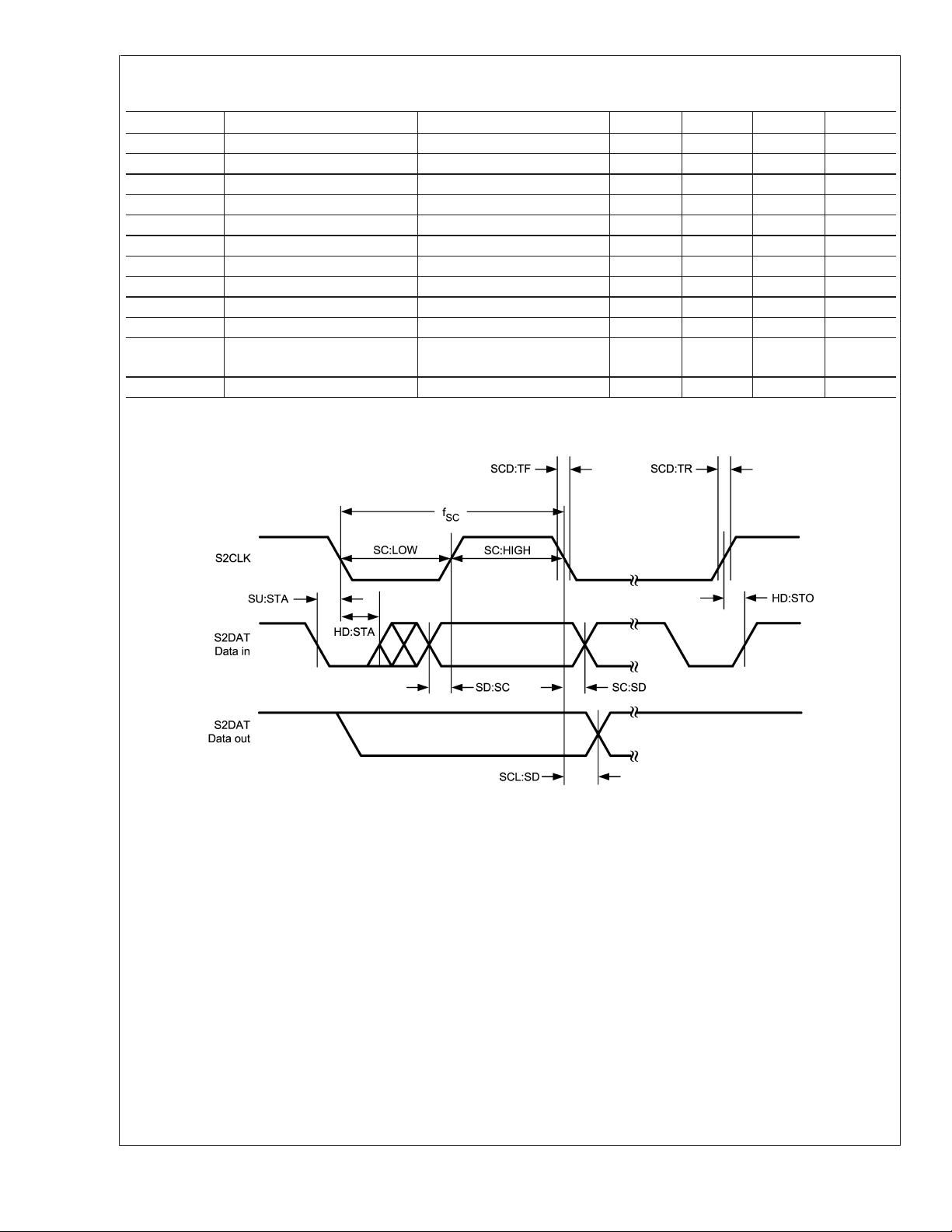
Two-Wire Serial Communication Interface
Over recommended operating supply and temperature ranges unless otherwise specified.
Symbol Parameter Conditions Min Typ Max Units
DS90C3202
f
SC
SC:LOW Clock Low Period R
SC:HIGH Clock High Period R
SCD:TR S2CLK and S2DAT Rise Time R
SCD:TF S2CLK and S2DAT Fall Time R
SU:STA Start Condition Setup Time R
HD:STA Start Condition Hold Time R
HD:STO Stop Condition Hold Time R
SC:SD Clock Falling Edge to Data R
SD:SC Data to Clock Rising Edge R
SCL:SD S2CLK Low to S2DAT Data
S2CLK Clock Frequency 400 kHz
= 4.7KΩ,CL= 50pF 1.5 us
P
= 4.7KΩ,CL= 50pF 0.6 us
P
= 4.7KΩ,CL= 50pF 0.3 us
P
= 4.7KΩ,CL= 50pF 0.3 us
P
= 4.7KΩ,CL= 50pF 0.6 us
P
= 4.7KΩ,CL= 50pF 0.6 us
P
= 4.7KΩ,CL= 50pF 0.6 us
P
= 4.7KΩ,CL= 50pF 0 us
P
= 4.7KΩ,CL= 50pF 0.1 us
P
R
= 4.7KΩ,CL= 50pF 0.1 0.9 us
P
Valid
BUF Bus Free Time RP= 4.7KΩ,CL= 50pF 13 us
AC Timing Diagrams
FIGURE 1. Two-Wire Serial Communication Interface Timing Diagram
www.national.com 6
20147122
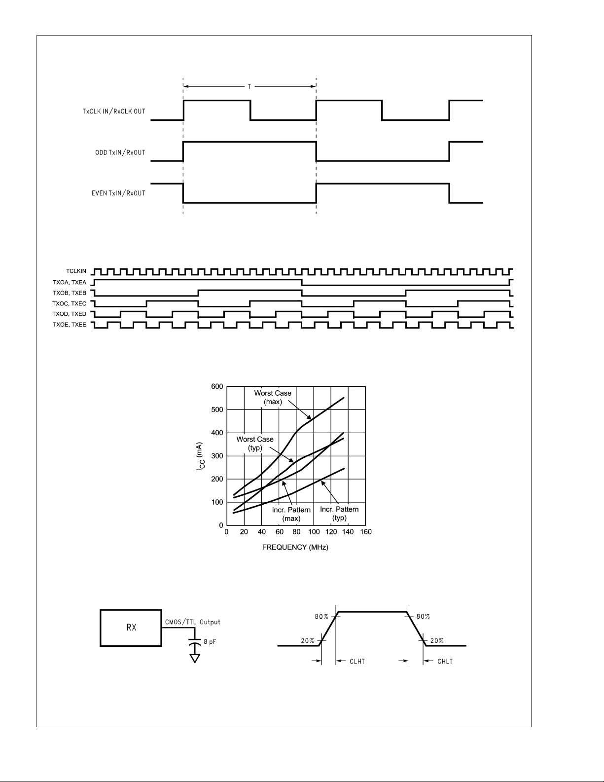
AC Timing Diagrams (Continued)
FIGURE 2. “Worst Case” Test Pattern
DS90C3202
20147103
FIGURE 3. Incremental Test Pattern
20147105
FIGURE 4. Typical and Max ICC with Worse Case and Incremental Pattern
20147104
FIGURE 5. LVCMOS/LVTTL Output Load and Transition Times
20147106
www.national.com7

AC Timing Diagrams (Continued)
DS90C3202
20147107
FIGURE 6. Receiver Phase Lock Loop Wake-up Time
FIGURE 7. Powerdown Delay
FIGURE 8. Receiver Propagation Delay
20147108
20147109
www.national.com 8

AC Timing Diagrams (Continued)
FIGURE 9. RFB: LVTTL Level Programmable Strobe Select
DS90C3202
20147110
RITOL ≥ Cable Skew (type, length) + Source Clock Jitter (cycle to cycle) (Note 11) + ISI (Inter-symbol interference) (Note 12)
Cable Skew — typically 10 ps–40 ps per foot, media dependent
Please see National’s AN-1217 for more details.
Note 11: Cycle-to-cycle jitter is less than 100 ps (worse case estimate).
Note 12: ISI is dependent on interconnect length; may be zero.
20147111
FIGURE 10. Receiver Input Tolerance and Sampling Window
Register address 29d/1dh bit [2:1] = 00b
20147112
FIGURE 11. Receiver RSRC and RHRC Output Setup/Hold Time — PTO Disabled
www.national.com9

AC Timing Diagrams (Continued)
DS90C3202
RegisterAddress 29d/1dh bit [2:1] = 00b
20147113
FIGURE 12. Receiver RSRC and RHRC Output Setup/Hold Time — PTO Enabled
FIGURE 13. Receiver RSRC and RHRC Output Setup/Hold Time Adjustment — PTO Disabled
www.national.com 10
20147114

AC Timing Diagrams (Continued)
DS90C3202
FIGURE 14. Receiver RSRC and RHRC Output Setup/Hold Time Adjustment — PTO Enabled
20147115
www.national.com11

AC Timing Diagrams (Continued)
DS90C3202
FIGURE 15. LVDS Input Mapping
www.national.com 12
20147116

AC Timing Diagrams (Continued)
DS90C3202
FIGURE 16. Receiver RITOL Min and Max
20147117
www.national.com13

Pin Diagram
DS90C3202
DS90C3202 Receiver
www.national.com 14
20147118

DS90C3202 Pin Descriptions
Pin No. Pin Name I/O Pin Type Description
1 S2DAT I/OP Digital Two-wire Serial Interface – Data
2 S2CLK I/P Digital Two-wire Serial Interface – Clock
3 VDDP1 VDD PLL Power supply for PLL circuitry
4 VSSP1 GND PLL Ground pin for PLL circuitry
5 VSSP0 GND PLL Ground pin for PLL circuitry
6 VDDP0 VDD PLL Power supply for PLL circuitry
7 PWDNB I/P LVTTL I/P (pulldown) Powerdown Bar (Active LOW)
0 = DEVICE DISABLED
1 = DEVICE ENABLED
8 RXEE0 O/P LVTTL O/P LVTTL level data output
9 RXEE1 O/P LVTTL O/P LVTTL level data output
10 RXEE2 O/P LVTTL O/P LVTTL level data output
11 RXEE3 O/P LVTTL O/P LVTTL level data output
12 RXEE4 O/P LVTTL O/P LVTTL level data output
13 RXEE5 O/P LVTTL O/P LVTTL level data output
14 RXEE6 O/P LVTTL O/P LVTTL level data output
15 VSS0 GND LVTTL O/P PWR Ground pin for LVTTL outputs and digital circuitry
16 VDD0 VDD LVTTL O/P PWR Power supply pin for LVTTL outputs and digital
circuitry
17 RXED0 O/P LVTTL O/P LVTTL level data output
18 RXED1 O/P LVTTL O/P LVTTL level data output
19 RXED2 O/P LVTTL O/P LVTTL level data output
20 RXED3 O/P LVTTL O/P LVTTL level data output
21 RXED4 O/P LVTTL O/P LVTTL level data output
22 RXED5 O/P LVTTL O/P LVTTL level data output
23 RXED6 O/P LVTTL O/P LVTTL level data output
24 VSSR0 GND RX LOGIC Ground pin for logic
25 VDDR0 VDD RX LOGIC Power supply for logic
26 RXEC0 O/P LVTTL O/P LVTTL level data output
27 RXEC1 O/P LVTTL O/P LVTTL level data output
28 RXEC2 O/P LVTTL O/P LVTTL level data output
29 RXEC3 O/P LVTTL O/P LVTTL level data output
30 RXEC4 O/P LVTTL O/P LVTTL level data output
31 RXEC5 O/P LVTTL O/P LVTTL level data output
32 VSS1 GND LVTTL O/P PWR Ground pin for LVTTL outputs and digital circuitry
33 VDD1 VDD LVTTL O/P PWR Power supply pin for LVTTL outputs and digital
circuitry
34 RXEC6 O/P LVTTL O/P LVTTL level data output
35 RXEB0 O/P LVTTL O/P LVTTL level data output
36 RXEB1 O/P LVTTL O/P LVTTL level data output
37 RXEB2 O/P LVTTL O/P LVTTL level data output
38 RXEB3 O/P LVTTL O/P LVTTL level data output
39 RXEB4 O/P LVTTL O/P LVTTL level data output
40 RXEB5 O/P LVTTL O/P LVTTL level data output
41 RXEB6 O/P LVTTL O/P LVTTL level data output
42 VSSR1 GND RX LOGIC Ground pin for logic
43 VDDR1 VDD RX LOGIC Power supply for logic
44 RCLKOUT O/P LVTTL O/P LVTTL level clock output
45 VSS2 GND LVTTL O/P PWR Ground pin for LVTTL outputs and digital circuitry
DS90C3202
www.national.com15

DS90C3202 Pin Descriptions (Continued)
Pin No. Pin Name I/O Pin Type Description
DS90C3202
46 VDD2 VDD LVTTL O/P PWR Power supply pin for LVTTL outputs and digital
circuitry
47 RXEA0 O/P LVTTL O/P LVTTL level data output
48 RXEA1 O/P LVTTL O/P LVTTL level data output
49 RXEA2 O/P LVTTL O/P LVTTL level data output
50 RXEA3 O/P LVTTL O/P LVTTL level data output
51 RXEA4 O/P LVTTL O/P LVTTL level data output
52 RXEA5 O/P LVTTL O/P LVTTL level data output
53 RXEA6 O/P LVTTL O/P LVTTL level data output
54 VSS3 GND LVTTL O/P PWR Ground pin for LVTTL outputs and digital circuitry
55 VDD3 VDD LVTTL O/P PWR Power supply pin for LVTTL outputs and digital
circuitry
56 RXOE0 O/P LVTTL O/P LVTTL level data output
57 RXOE1 O/P LVTTL O/P LVTTL level data output
58 RXOE2 O/P LVTTL O/P LVTTL level data output
59 RXOE3 O/P LVTTL O/P LVTTL level data output
60 RXOE4 O/P LVTTL O/P LVTTL level data output
61 RXOE5 O/P LVTTL O/P LVTTL level data output
62 RXOE6 O/P LVTTL O/P LVTTL level data output
63 RXOD0 O/P LVTTL O/P LVTTL level data output
64 VSS4 GND LVTTL O/P PWR Ground pin for LVTTL outputs and digital circuitry
65 VDD4 VDD LVTTL O/P PWR Power supply pin for LVTTL outputs and digital
circuitry
66 RXOD1 O/P LVTTL O/P LVTTL level data output
67 RXOD2 O/P LVTTL O/P LVTTL level data output
68 RXOD3 O/P LVTTL O/P LVTTL level data output
69 RXOD4 O/P LVTTL O/P LVTTL level data output
70 RXOD5 O/P LVTTL O/P LVTTL level data output
71 RXOD6 O/P LVTTL O/P LVTTL level data output
72 RXOC0 O/P LVTTL O/P LVTTL level data output
73 RXOC1 O/P LVTTL O/P LVTTL level data output
74 RXOC2 O/P LVTTL O/P LVTTL level data output
75 RXOC3 O/P LVTTL O/P LVTTL level data output
76 RXOC4 O/P LVTTL O/P LVTTL level data output
77 RXOC5 O/P LVTTL O/P LVTTL level data output
78 RXOC6 O/P LVTTL O/P LVTTL level data output
79 RXOB0 O/P LVTTL O/P LVTTL level data output
80 RXOB1 O/P LVTTL O/P LVTTL level data output
81 RXOB2 O/P LVTTL O/P LVTTL level data output
82 RXOB3 O/P LVTTL O/P LVTTL level data output
83 RXOB4 O/P LVTTL O/P LVTTL level data output
84 RXOB5 O/P LVTTL O/P LVTTL level data output
85 RXOB6 O/P LVTTL O/P LVTTL level data output
86 VDDR2 VDD RX LOGIC Power supply for logic
87 VSSR2 GND RX LOGIC Ground pin for logic
88 RXOA0 O/P LVTTL O/P LVTTL level data output
89 RXOA1 O/P LVTTL O/P LVTTL level data output
90 RXOA2 O/P LVTTL O/P LVTTL level data output
91 RXOA3 O/P LVTTL O/P LVTTL level data output
www.national.com 16

DS90C3202 Pin Descriptions (Continued)
Pin No. Pin Name I/O Pin Type Description
92 RXOA4 O/P LVTTL O/P LVTTL level data output
93 RXOA5 O/P LVTTL O/P LVTTL level data output
94 RXOA6 O/P LVTTL O/P LVTTL level data output
95 VDD5 VDD LVTTL O/P PWR Power supply pin for LVTTL outputs and digital
circuitry
96 VSS5 GND LVTTL O/P PWR Ground pin for LVTTL outputs and digital circuitry
97 RESRVD I/P LVTTL I/P (pulldown) Tie to VSS for correct functionality
98 MODE1 I/P Digital (pulldown) “ODD” Bank Enable
0 = LVTTL ODD OUTPUTS DISABLED
(Data Output Low)
1 = LVTTL ODD OUTPUTS ENABLED
99 VSSL GND LVDS PWR Ground pin for LVDS
100 VDDL VDD LVDS PWR Power supply pin for LVDS
101 RXOA- I/P LVDS I/P Negative LVDS differential data input
102 RXOA+ I/P LVDS I/P Positive LVDS differential data input
103 RXOB- I/P LVDS I/P Negative LVDS differential data input
104 RXOB+ I/P LVDS I/P Positive LVDS differential data input
105 RXOC- I/P LVDS I/P Negative LVDS differential data input
106 RXOC+ I/P LVDS I/P Positive LVDS differential data input
107 RXOD- I/P LVDS I/P Negative LVDS differential data input
108 RXOD+ I/P LVDS I/P Positive LVDS differential data input
109 RXOE- I/P LVDS I/P Negative LVDS differential data input
110 RXOE+ I/P LVDS I/P Positive LVDS differential data input
111 VSSL GND LVDS PWR Ground pin for LVDS
112 VSSL GND LVDS PWR Ground pin for LVDS
113 VDDL VDD LVDS PWR Power supply pin for LVDS
114 VDDL VDD LVDS PWR Power supply pin for LVDS
115 RCLKIN- I/P LVDS I/P Negative LVDS differential clock input
116 RCLKIN+ I/P LVDS I/P Positive LVDS differential clock input
117 RXEA- I/P LVDS I/P Negative LVDS differential data input
118 RXEA+ I/P LVDS I/P Positive LVDS differential data input
119 RXEB- I/P LVDS I/P Negative LVDS differential data input
120 RXEB+ I/P LVDS I/P Positive LVDS differential data input
121 RXEC- I/P LVDS I/P Negative LVDS differential data input
122 RXEC+ I/P LVDS I/P Positive LVDS differential data input
123 RXED- I/P LVDS I/P Negative LVDS differential data input
124 RXED+ I/P LVDS I/P Positive LVDS differential data input
125 RXEE- I/P LVDS I/P Negative LVDS differential data input
126 RXEE+ I/P LVDS I/P Positive LVDS differential data input
127 MODE0 I/P Digital (pulldown) “EVEN” Bank Enable
0 = LVTTL EVEN OUTPUTS DISABLED
(Data Output Low)
1 = LVTTL EVEN OUTPUTS ENABLED
128 RFB I/P Digital (pulldown) Rising Falling Bar (Figure 9)
0 = FALLING EDGE DATA STROBE
1 = RISING EDGE DATA STROBE
DS90C3202
www.national.com17

Two-Wire Serial Communication Interface Description
The DS90C3202 operates as a slave on the Serial Bus, so
DS90C3202
the S2CLK line is an input (no clock is generated by the
DS90C3202) and the S2DAT line is bi-directional.
DS90C3202 has a fixed 7bit slave address. The address is
not user configurable in anyway.
A zero in front of the register address is required. For example, to access register 0x0Fh, “0F” is the correct way of
accessing the register.
COMMUNICATING WITH THE DS90C3202 CONTROL REGISTERS
There are 32 data registers (one byte each) in the
DS90C3202, and can be accessed through 32 addresses.
All registers are predefined as read only or read and write.
The DS90C3202 slave state machine does not require an
internal clock and it supports only byte read and write. Page
mode is not supported. The 7bit binary address is 0111110
All seven bits are hardwired internally.
Reading the DS90C3202 can take place either of three ways:
1. If the location latched in the data register addresses is
correct, then the read can simply consist of a slave
address byte, followed by retrieving the data byte.
2. If the data register address needs to be set, then a slave
address byte, data register address will be sent first,
then the master will repeat start, send the slave address
byte and data byte to accomplish a read.
3. When performing continuous read operations, another
write (or read) instruction in between reads needs to be
completed in order for the two-wire serial interface module to read repeatedly.
The data byte has the most significant bit first. At the end of
a read, the DS90C3202 can accept either Acknowledge or
No Acknowledge from the Master (No Acknowledge is typically used as a signal for the slave that the Master has read
its last byte).
FIGURE 17. Byte Read
The master must generate a Start by sending the 7-bit slave
address plus a 0 first, and wait for acknowledge from
DS90C3202. When DS90C3202 acknowledges (the 1st
ACK) that the master is calling, the master then sends the
data register address byte and waits for acknowledge from
the slave. When the slave acknowledges (the 2nd ACK), the
master repeats the “Start” by sending the 7-bit slave address
plus a 1 (indicating that READ operation is in progress) and
FIGURE 18. Byte Write
20147119
waits for acknowledge from DS90C3202. After the slave
responds (the 3rd ACK), the slave sends the data to the bus
and waits for acknowledge from the master. When the master acknowledges (the 4th ACK), it generates a “Stop”. This
completes the “ READ”.
A Write to the DS90C3202 will always include the slave
address, data register address byte, and a data byte.
20147120
The master must generate a “Start” by sending the 7-bit
slave address plus a 0 and wait for acknowledge from
DS90C3202. When DS90C3202 acknowledges (the 1st
ACK) that the master is calling, the master then sends the
data register address byte and waits for acknowledge from
www.national.com 18
the slave. When the slave acknowledges (the 2nd ACK), the
master sends the data byte and wait for acknowledge from
the slave. When the slave acknowledges (the 3rd ACK), the
master generates a “ Stop”. This completes the “WRITE”.

DS90C3202 Two-Wire Serial Interface Register Table
Address R/W RESET Bit # Description Default Value
0d/0h R PWDN [7:0] Vender ID low byte[7:0] = 05h 0000_0101
1d/1h R PWDN [7:0] Vender ID high byte[15:8] =13h 0001_0011
2d/2h R PWDN [7:0] Device ID low byte[7:0] = 28h 0010_1000
3d/3h R PWDN [7:0] Device ID high byte 15:8] = 67h 0110_0111
4d/4h R PWDN [7:0] Device revision [7:0] = 00h to begin with 0000_0000
5d/5h R PWDN [7:0] Low frequency limit, 8Mhz = 8h 0000_1000
6d/6h R PWDN [7:0] High frequency limit 135Mhz = 87h =
0000_0000_1000_0111
7d/7h R PWDN [7:0] Reserved 0000_0000
8d/8h R PWDN [7:0] Reserved 0000_0000
9d/9h R PWDN [7:0] Reserved 0000_0000
10d/ah R PWDN [7:0] Reserved 0000_0000
11d/bh R PWDN [7:0] Reserved 0000_0000
20d/14h R/W None [7:0] Reserved 0000_0000
21d/15h R/W None [7:0] Reserved 0000_0000
22d/16h R/W None [7:3] Reserved 0000_0000
[2:0] LVDS input skew control for CLK channel,
000 (default) applies to no delay added, ONE buffer
delay per step adjustment towards Tsetup improvement
23d/17h R/W None [7] Reserved 0000_0000
[6:4] LVDS input skew control for RXO channel B,
000 (default) applies to no delay added, ONE buffer
delay per step adjustment towards Thold improvements
[3] Reserved
[2:0] LVDS input skew control for RXO channel C,
000 (default) applies to no delay added, ONE buffer
delay per step adjustment towards Thold improvements
24d/18h R/W None [7] Reserved 0000_0000
[6:4] LVDS input skew control for RXO channel D,
000 (default) applies to no delay added, ONE buffer
delay per step adjustment towards Thold improvements
[3] Reserved
[2:0] LVDS input skew control for RXO channel E,
000 (default) applies to no delay added, ONE buffer
delay per step adjustment towards Thold improvements
25d/19h R/W None [7] Reserved 0000_0000
[6:4] LVDS input skew control for RXO channel A,
000 (default) applies to no delay added, ONE buffer
delay per step adjustment towards Thold improvements
[3] Reserved
[2:0] LVDS input skew control for RXE channel A,
000 (default) applies to no delay added, ONE buffer
delay per step adjustment towards Thold improvements
1000_0111
DS90C3202
www.national.com19

DS90C3202 Two-Wire Serial Interface Register Table (Continued)
Address R/W RESET Bit # Description Default Value
26d/1ah R/W None [7] Reserved 0000_0000
DS90C3202
[6:4] LVDS input skew control for RXE channel B,
000 (default) applies to no delay added, ONE buffer
delay per step adjustment towards Thold improvements
[3] Reserved
[2:0] LVDS input skew control for RXE channel C,
000 (default) applies to no delay added, ONE buffer
delay per step adjustment towards Thold improvements
27d/1bh R/W None [7] Reserved 0000_0000
[6:4] LVDS input skew control for RXE channel D,
000 (default) applies to no delay added, ONE buffer
delay per step adjustment
[3] Reserved
[2:0] LVDS input skew control for RXE channel E,
000 (default) applies to no delay added, ONE buffer
delay per step adjustment towards Thold improvements
28d/1ch R/W None [7:3] Reserved 0000_0000
[2] LVTTL output transition time control for CLK
0: Tr/Tf = 1.0ns (default)
1: Tr/Tf = 1.5ns
[1] LVTTL output transition time control for RXE
0: Tr/Tf = 1.5ns (default)
1: Tr/Tf = 2.5ns
[0] LVTTL output transition time control for RXO
0: Tr/Tf = 1.5ns (default)
1: Tr/Tf = 2.5ns
29d/1dh R/W None [7:3] Reserved 0000_0000
[2:1] LVTTL output setup and hold time control
00: balanced setup and hold time (default)
01: setup time is increased from default position by 1UI
& hold time is reduced from default position by 1UI
10: setup time is decreased from default position by 1UI
& hold time is reduced from default position by 1UI
11: setup time is increased from default position by 2UI
& hold time is increased from default position by 2UI
[0] LVTTL output PTO control
1: PTO disabled, all outputs setup time are only
controlled by contents of [2:1]
0: PTO enabled (default)
Group1: CLK to latch Data is re-assigned earlier by
0.5UI respect to the normal centered position if only
PTO option enabled; but PTO option and (Tsetup or
Thold) adjustment can co-exist
Group2: CLK to latch Data stays as the normal
centered position if only PTO option enabled; but PTO
option and (Tsetup or Thold) adjustment can co-exist
www.national.com 20

DS90C3202 Two-Wire Serial Interface Register Table (Continued)
Address R/W RESET Bit # Description Default Value
30d/1eh R/W None [7:5] Reserved 0000_0000
[4] I/O disable control for RXE channel A,
1: disable, 0: enable (default)
[3] I/O disable control for RXE channel B,
1: disable, 0: enable (default)
[2] I/O disable control for RXE channel C,
1: disable, 0: enable (default)
[1] I/O disable control for RXE channel D,
1: disable, 0: enable (default)
[0] I/O disable control for RXE channel E,
1: disable, 0: enable (default)
31d/1fh R/W None [7:6] 11; LVTTL Outputs available as long as "NO CLK" is at
HIGH regardless PLL lock or not
10; LVTTL Outputs available after 1K of CLK cycles
detected & PLL generated strobes are within 0.5UI
respect to REFCLK
01; LVTLL Outputs available after 2K of CLK cycles
detected
00: default ; LVTTL Outputs available after 1K of CLK
cycles detected
[5] 0: default; to select the size of wait counter between 1K
or 2K, default is 1K
[4] I/O disable control for RXO channel A,
1: disable, 0: enable (default)
[3] I/O disable control for RXO channel B,
1 disable, 0: enable (default)
[2] I/O disable control for RXO channel C,
1: disable, 0: enable (default)
[1] I/O disable control for RXO channel D,
1: disable, 0: enable (default)
[0] I/O disable control for RXO channel E,
1: disable, 0: enable (default)
Note 13: Registers with RESET designated with “None” requires device to be power cycled to reset register values to their default state.
0000_0000
DS90C3202
www.national.com21

Physical Dimensions inches (millimeters) unless otherwise noted
128-Pin TQFP Package
Order Number DS90C3202VS
NS Package Number VJX128A
DS90C3202 3.3V 8 MHz to 135 MHz Dual FPD-Link Receiver
National does not assume any responsibility for use of any circuitry described, no circuit patent licenses are implied and National reserves
the right at any time without notice to change said circuitry and specifications.
For the most current product information visit us at www.national.com.
LIFE SUPPORT POLICY
NATIONAL’S PRODUCTS ARE NOT AUTHORIZED FOR USE AS CRITICAL COMPONENTS IN LIFE SUPPORT DEVICES OR SYSTEMS
WITHOUT THE EXPRESS WRITTEN APPROVAL OF THE PRESIDENT AND GENERAL COUNSEL OF NATIONAL SEMICONDUCTOR
CORPORATION. As used herein:
1. Life support devices or systems are devices or systems
which, (a) are intended for surgical implant into the body, or
(b) support or sustain life, and whose failure to perform when
properly used in accordance with instructions for use
provided in the labeling, can be reasonably expected to result
in a significant injury to the user.
BANNED SUBSTANCE COMPLIANCE
National Semiconductor follows the provisions of the Product Stewardship Guide for Customers (CSP-9-111C2) and Banned Substances
and Materials of Interest Specification (CSP-9-111S2) for regulatory environmental compliance. Details may be found at:
www.national.com/quality/green.
Lead free products are RoHS compliant.
National Semiconductor
Americas Customer
Support Center
Email: new.feedback@nsc.com
Tel: 1-800-272-9959
www.national.com
National Semiconductor
Europe Customer Support Center
Fax: +49 (0) 180-530 85 86
Email: europe.support@nsc.com
Deutsch Tel: +49 (0) 69 9508 6208
English Tel: +44 (0) 870 24 0 2171
Français Tel: +33 (0) 1 41 91 8790
2. A critical component is any component of a life support
device or system whose failure to perform can be reasonably
expected to cause the failure of the life support device or
system, or to affect its safety or effectiveness.
National Semiconductor
Asia Pacific Customer
Support Center
Email: ap.support@nsc.com
National Semiconductor
Japan Customer Support Center
Fax: 81-3-5639-7507
Email: jpn.feedback@nsc.com
Tel: 81-3-5639-7560
 Loading...