

查询DS90C3201供应商
ADVANCE INFORMATION
DS90C3201
3.3V 8 MHz to 135 MHz Dual FPD-Link Transmitter
DS90C3201 3.3V 8 MHz to 135 MHz Dual FPD-Link Transmitter
April 2005
General Description
The DS90C3201 is a 3.3V single/dual FPD-Link 10-bit color
transmitter is designed to be used in Liquid Crystal Display
TVs, LCD Monitors, Digital TVs, and Plasma Display Panel
TVs. The DS90C3201 is designed to interface between the
digital video processor and the display device using the
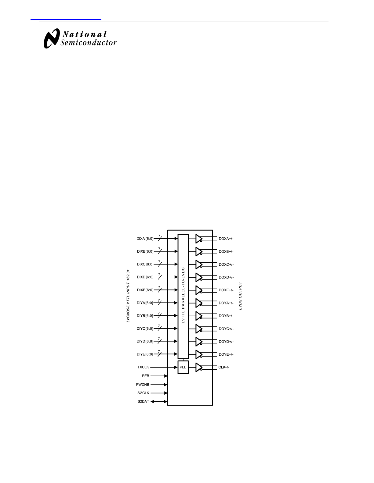
low-power, low-EMI LVDS (Low Voltage Differential Signaling) interface. The DS90C3201 converts up to 70 bits of
LVCMOS/LVTTL data into ten LVDS data streams. The
transmitter can be programmed clocking data with rising
edge or falling edge clock. Optional two-wire serial programming allows fine tuning in development and production environments. At a transmitted clock frequency of 135 MHz, 70
bits of LVCMOS/LVTTL data are transmitted at an effective
rate of 945 Mbps per LVDS channel. Using a 135 MHz clock,
the data throughput is 9.45Gbit/s (945Mbytes/s). This allows
the dual 10-bit LVDS Transmitter to support HDTV resolutions.
Block Diagram
Features
n Up to 9.45Gbit/s data throughput
n 8 MHz to 135 MHz input clock support
n Supports up to QXGA panel resolutions
n Supports HDTV resolutions and frame rates up to
1920 x 1080p
n LVDS 30-bit, 24-bit or 18-bit color data outputs
n Supports single pixel and dual pixel interfaces
n Supports spread spectrum clocking
n Two-wire serial communication interface
n Programmable clock edge and control strobe select
n Power down mode
n +3.3V supply voltage
n 128-pin TQFP
n Compliant to TIA/EIA-644-A-2001 LVDS Standard
n Backward compatible configuration with FPD-Link
FIGURE 1. Transmitter Block Diagram
© 2005 National Semiconductor Corporation DS201472 www.national.com
20147201
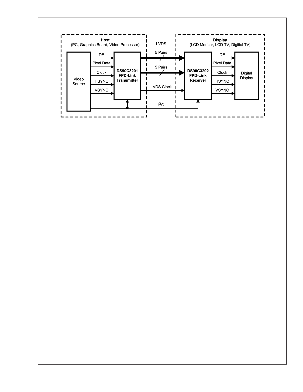
Typical Application Diagram
DS90C3201
FIGURE 2. LCD Panel Application Diagram
Functional Description
The DS90C3201 and DS90C3202 are a dual 10-bit color
Transmitter and Receiver FPD-Link chipset designed to
transmit data at clocks speeds from 8 to 135 MHz.
DS90C3201 and DS90C3202 are designed to interface between the digital video processor and the display using a
LVDS interface. The DS90C3201 transmitter serializes 2
channels of video data (10-bit each for RGB for each channel, totaling 60 bits) and control signals (HSYNC, VSYNC,
DE and two user-defined signals) along with clock signal to
10 channels of LVDS signals and transmits them. The
DS90C3202 receiver converts 10 channels of LVDS signals
into parallel signals and outputs 2 channels of video data
(10-bit each for RGB for each channel, totaling 60 bits) and
control signals (HSYNC, VSYNC, DE and two user-defined
signals) along with clock signal. The dual high speed LVDS
channels supports single pixel in-single pixel out and dual
pixel in-dual pixel out transmission modes. The FPD-Link
chipset is suitable for a variety of display applications including LCD Monitors, LCD TV, Digital TV, and DLP TV, and
Plasma Display Panels.
Using a true 10-bit color depth system, the 30-bit RGB color
produces over 1.07 billion colors to represent High Definition
(HD) displays in their most natural color, surpassing the
maximum 16.7 million colors achieved by 6/8-bit color conventionally used for large-scale LCD televisions and LCD
monitors.
LVDS TRANSMITTER
The LVDS Transmitter serializes LVCMOS/LVTTL RGB
video data and control signal timing into LVDS data streams.
SINGLE PIXEL AND DUAL PIXEL INTERFACE
The DS90C3201 LVDS ports support two modes: Single
Pixel mode (30-bit LVDS output) and Dual Pixel mode (2 x
30-bit LVDS output). For Single Pixel mode, LVDS ports
20147202
DOX[A-E] for 10-bit RGB data are utilized. For the Dual Pixel
mode, both DOX[A-E] and DOY[A-E] LVDS ports for odd and
even 10-bit RGB data are utilized.
SELECTABLE INPUT DATA STROBE
The Transmitter input data edge strobe can be latched on
the rising or falling edges of input clock signal. The dedicated
RFB pin is used to program input strobe select on the rising
edge of TXCLK or the falling edge of TXCLK.
2-WIRE SERIAL COMMUNICATION INTERFACE
Optional I2C programming allows fine tuning in development
and production environments. The I2C interface provides
several capabilities to reduce EMI and to customize output
timing. These capabilities are selectable/programmable via
I2C: Programmable LVDS Swing Control, Adjustable Input
Setup/Hold Control, Input/Output Channel Control.
PROGRAMMABLE LVDS SWING CONTROL
Programmable LVDS amplitude (VOD) and LVDS offset voltage (VOS) of the differential signals can be adjusted for
better impedance matching for noise and EMI reduction. The
low level LVDS swing mode and offset voltage can be controlled via I2C.
ADJUSTABLE INPUT SETUP/HOLD CONTROL
Programmable LVCMOS/LVTTL Data Input Setup and Hold
Times can be adjusted with respect to TXCLK for convenient
interface with a variety of graphic controllers and video processors. Feature is controlled via I2C.
INPUT/OUTPUT CHANNEL CONTROL
Full independent control for input/output channels can be
disabled to minimize power supply line noise and overall
power dissipation. Feature is configured via I2C.
www.national.com 2

Physical Dimensions inches (millimeters) unless otherwise noted
DS90C3201 3.3V 8 MHz to 135 MHz Dual FPD-Link Transmitter
128-Pin TQFP Package
Order Number DS90C3201VS
NS Package Number VJX128A
National does not assume any responsibility for use of any circuitry described, no circuit patent licenses are implied and National reserves
the right at any time without notice to change said circuitry and specifications.
For the most current product information visit us at www.national.com.
LIFE SUPPORT POLICY
NATIONAL’S PRODUCTS ARE NOT AUTHORIZED FOR USE AS CRITICAL COMPONENTS IN LIFE SUPPORT DEVICES OR SYSTEMS
WITHOUT THE EXPRESS WRITTEN APPROVAL OF THE PRESIDENT AND GENERAL COUNSEL OF NATIONAL SEMICONDUCTOR
CORPORATION. As used herein:
1. Life support devices or systems are devices or systems
which, (a) are intended for surgical implant into the body, or
(b) support or sustain life, and whose failure to perform when
properly used in accordance with instructions for use
2. A critical component is any component of a life support
device or system whose failure to perform can be reasonably
expected to cause the failure of the life support device or
system, or to affect its safety or effectiveness.
provided in the labeling, can be reasonably expected to result
in a significant injury to the user.
BANNED SUBSTANCE COMPLIANCE
National Semiconductor manufactures products and uses packing materials that meet the provisions of the Customer Products
Stewardship Specification (CSP-9-111C2) and the Banned Substances and Materials of Interest Specification (CSP-9-111S2) and contain
no ‘‘Banned Substances’’ as defined in CSP-9-111S2.
National Semiconductor
Americas Customer
Support Center
Email: new.feedback@nsc.com
Tel: 1-800-272-9959
www.national.com
National Semiconductor
Europe Customer Support Center
Fax: +49 (0) 180-530 85 86
Email: europe.support@nsc.com
Deutsch Tel: +49 (0) 69 9508 6208
English Tel: +44 (0) 870 24 0 2171
Français Tel: +33 (0) 1 41 91 8790
National Semiconductor
Asia Pacific Customer
Support Center
Email: ap.support@nsc.com
National Semiconductor
Japan Customer Support Center
Fax: 81-3-5639-7507
Email: jpn.feedback@nsc.com
Tel: 81-3-5639-7560
 Loading...