

查询DS90C032供应商
DS90C032
LVDS Quad CMOS Differential Line Receiver
DS90C032 LVDS Quad CMOS Differential Line Receiver
September 2003
General Description
TheDS90C032 is a quad CMOS differential line receiver
designed for applications requiring ultra low power dissipation and high data rates. The device is designed to support
data rates in excess of 155.5 Mbps (77.7 MHz) utilizing Low
Voltage Differential Signaling (LVDS) technology.
TheDS90C032 accepts low voltage (350 mV) differential
input signals and translates them to CMOS (TTL compatible)
output levels. The receiver supports a TRI-STATE
that may be used to multiplex outputs. The receiver also
supports OPEN, shorted and terminated (100Ω) input Failsafe with the addition of external failsafe biasing. Receiver
output will be HIGH for both Failsafe conditions.
TheDS90C032 and companion line driver (DS90C031) provide a new alternative to high power psuedo-ECL devices for
high speed point-to-point interface applications.
®
function
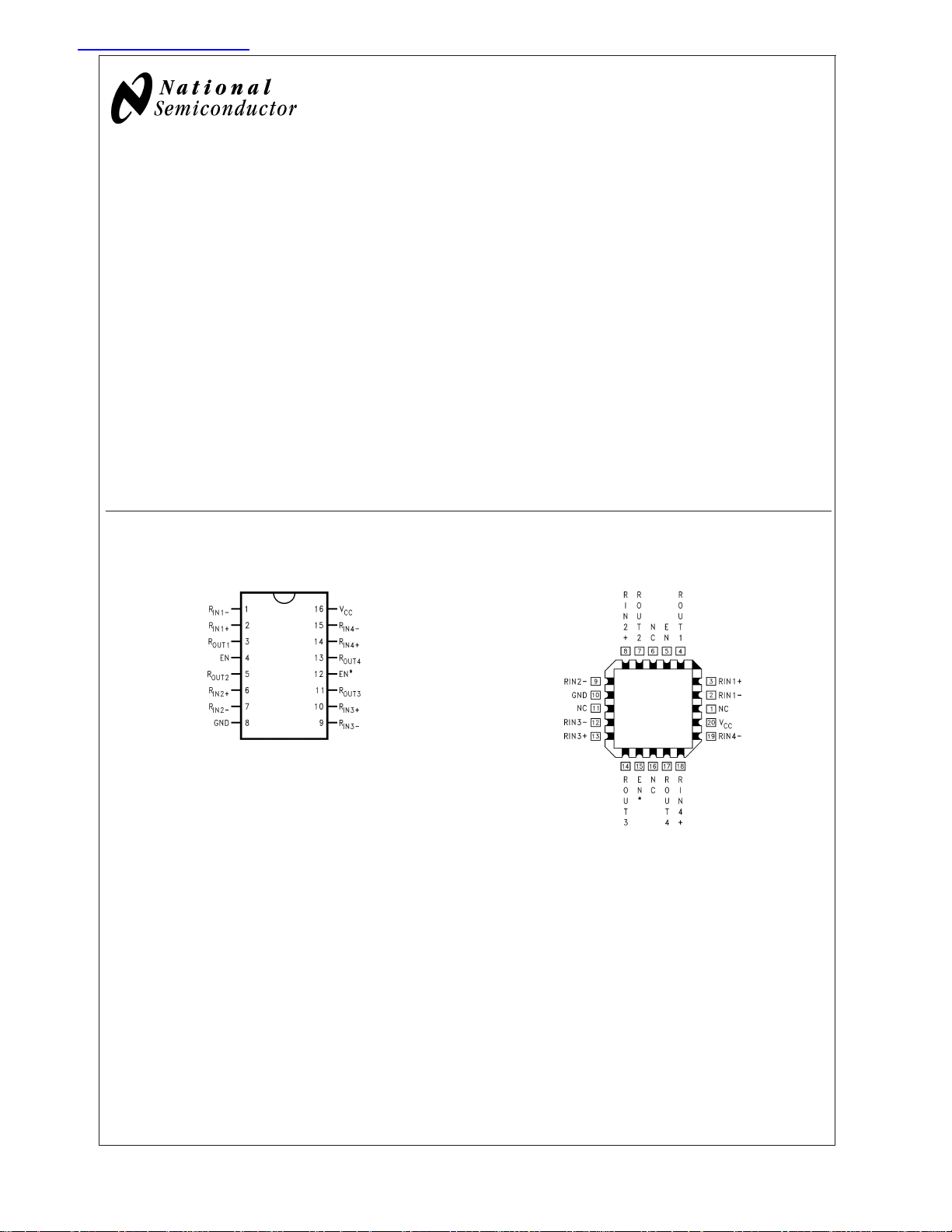
Connection Diagrams
Dual-In-Line
Features
n>155.5 Mbps (77.7 MHz) switching rates
n Accepts small swing (350 mV) differential signal levels
n Ultra low power dissipation
n 600 ps maximum differential skew (5V, 25˚C)
n 6.0 ns maximum propagation delay
n Industrial operating temperature range
n Military operating temperature range option
n Available in surface mount packaging (SOIC) and (LCC)
n Pin compatible with DS26C32A, MB570 (PECL) and
41LF (PECL)
n Supports OPEN, short and terminated input fail-safe
n Compatible with IEEE 1596.3 SCI LVDS standard
n Conforms to ANSI/TIA/EIA-644 LVDS standard
n Available to Standard Microcircuit Drawing (SMD)
5962-95834
LCC Package
Order Number
DS90C032TM
See NS Package Number M16A
TRI-STATE®is a registered trademark of National Semiconductor Corporation.
© 2003 National Semiconductor Corporation DS011945 www.national.com
01194501
01194520
Order Number
DS90C032E-QML
See NS Package Number E20A
For complete Military Specifications,
refer to appropriate SMD or MDS.
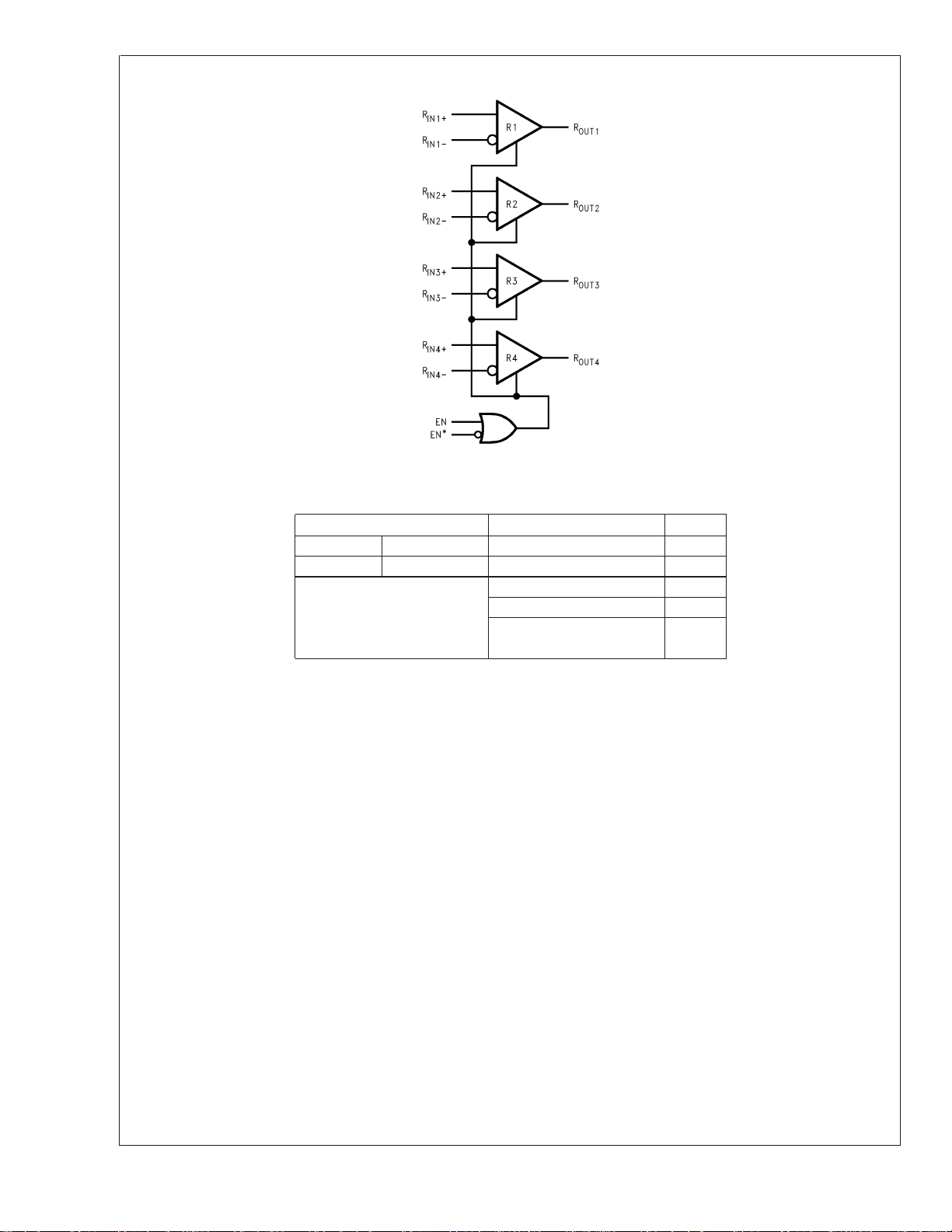
Functional Diagram and Truth Tables
DS90C032
Receiver
ENABLES INPUTS OUTPUT
EN EN* R
LH X Z
All other combinations V
of ENABLE inputs V
01194502
IN+−RIN−
≥ 0.1V H
ID
≤ −0.1V L
ID
R
Full Fail-safe OPEN/SHORT H
or Terminated
OUT
www.national.com 2
DS90C032
Absolute Maximum Ratings (Note 1)
If Military/Aerospace specified devices are required,
please contact the National Semiconductor Sales Office/
Distributors for availability and specifications.
Supply Voltage (V
Input Voltage (R
Enable Input Voltage
(EN, EN*) −0.3V to (V
Output Voltage (R
Maximum Package Power Dissipation
M Package 1025 mW
E Package 1830 mW
Derate M Package 8.2 mW/˚C above +25˚C
Derate E Package 12.2 mW/˚C above +25˚C
Storage Temperature Range −65˚C to +150˚C
Lead Temperature Range
Soldering (4 sec.) +260˚C
) −0.3V to +6V
CC
IN+,RIN−
) −0.3V to (VCC+0.3V)
) −0.3V to (VCC+0.3V)
OUT
@
+25˚C
CC
+0.3V)
Maximum Junction
Temperature (DS90C032T) +150˚C
Maximum Junction
Temperature (DS90C032E) +175˚C
ESD Rating (Note 7)
(HBM, 1.5 kΩ, 100 pF) ≥ 3,500V
(EIAJ, 0 Ω, 200 pF) ≥ 250V
Recommended Operating
Conditions
Min Typ Max Units
Supply Voltage (V
Receiver Input Voltage GND 2.4 V
Operating Free Air Temperature (T
DS90C032T −40 +25 +85 ˚C
DS90C032E −55 +25 +125 ˚C
) +4.5 +5.0 +5.5 V
CC
)
A
Electrical Characteristics
Over Supply Voltage and Operating Temperature ranges, unless otherwise specified. (Note 2)
Symbol Parameter Conditions Pin Min Typ Max Units
V
V
I
V
V
I
I
V
V
I
V
I
I
TH
TL
IN
OH
OL
OS
OZ
IH
IL
I
CL
CC
CCZ
Differential Input High Threshold VCM= +1.2V R
Differential Input Low Threshold −100 mV
Input Current VIN= +2.4V VCC= 5.5V −10
V
= 0V −10
IN
Output High Voltage IOH= −0.4 mA, VID= +200 mV R
I
= −0.4 mA, DS90C032T 3.8 4.9 V
OH
,
IN+
R
IN−
3.8 4.9 V
OUT
+100 mV
±
1 +10 µA
±
1 +10 µA
Input terminated
Output Low Voltage IOL= 2 mA, VID= −200 mV 0.07 0.3 V
Output Short Circuit Current Enabled, V
Output TRI-STATE Current Disabled, V
Input High Voltage EN,
Input Low Voltage 0.8 V
Input Current −10
= 0V (Note 8) −15 −60 −100 mA
OUT
OUT
=0VorV
CC
−10
±
1 +10 µA
2.0 V
EN*
±
1 +10 µA
Input Clamp Voltage ICL= −18 mA −1.5 −0.8 V
No Load Supply Current EN, EN* = VCCor GND, DS90C032T V
CC
3.5 10 mA
Receivers Enabled Inputs Open DS90C032E 3.5 11 mA
EN, EN* = 2.4 or 0.5, Inputs Open 3.7 11 mA
No Load Supply Current EN = GND, EN* = V
CC
DS90C032T 3.5 10 mA
Receivers Disabled Inputs Open DS90C032E 3.5 11 mA
www.national.com3

Switching Characteristics
VCC= +5.0V, TA= +25˚C DS90C032T (Notes 3, 4, 5, 9)
Symbol Parameter Conditions Min Typ Max Units
DS90C032
t
PHLD
t
PLHD
t
SKD
t
SK1
t
TLH
t
THL
t
PHZ
t
PLZ
t
PZH
t
PZL
Differential Propagation Delay High to Low CL= 5 pF 1.5 3.40 5.0 ns
Differential Propagation Delay Low to High VID= 200 mV 1.5 3.48 5.0 ns
Differential Skew |t
PHLD−tPLHD
|(Figure 1 and Figure 2) 0 80 600 ps
Channel-to-Channel Skew (Note 5) 0 0.6 1.0 ns
Rise Time 0.5 2.0 ns
Fall Time 0.5 2.0 ns
Disable Time High to Z RL=2kΩ 10 15 ns
Disable Time Low to Z CL=10pF 10 15 ns
Enable Time Z to High (Figure 3 and Figure 4) 4 10 ns
Enable Time Z to Low 410ns
Switching Characteristics
VCC= +5.0V±10%, TA= −40˚C to +85˚C DS90C032T (Notes 3, 4, 5, 6, 9)
Symbol Parameter Conditions Min Typ Max Units
t
PHLD
t
PLHD
t
SKD
t
SK1
t
SK2
t
TLH
t
THL
t
PHZ
t
PLZ
t
PZH
t
PZL
Differential Propagation Delay High to Low CL= 5 pF 1.0 3.40 6.0 ns
Differential Propagation Delay Low to High VID= 200 mV 1.0 3.48 6.0 ns
Differential Skew |t
PHLD−tPLHD
|(Figure 1 and Figure 2) 0 0.08 1.2 ns
Channel-to-Channel Skew (Note 5) 0 0.6 1.5 ns
Chip to Chip Skew (Note 6) 5.0 ns
Rise Time 0.5 2.5 ns
Fall Time 0.5 2.5 ns
Disable Time High to Z RL=2kΩ 10 20 ns
Disable Time Low to Z CL=10pF 10 20 ns
Enable Time Z to High (Figure 3 and Figure 4) 4 15 ns
Enable Time Z to Low 415ns
Switching Characteristics
VCC= +5.0V±10%, TA= −55˚C to +125˚C DS90C032E (Notes 3, 4, 5, 6, 9, 10)
Symbol Parameter Conditions Min Typ Max Units
t
PHLD
t
PLHD
t
SKD
t
SK1
t
SK2
t
PHZ
t
PLZ
t
PZH
t
PZL
Differential Propagation Delay High to Low CL= 20 pF 1.0 3.40 8.0 ns
Differential Propagation Delay Low to High VID= 200 mV 1.0 3.48 8.0 ns
Differential Skew |t
PHLD−tPLHD
|(Figure 1 and Figure 2) 0 0.08 3.0 ns
Channel-to-Channel Skew (Note 5) 0 0.6 3.0 ns
Chip to Chip Skew (Note 6) 7.0 ns
Disable Time High to Z RL=2kΩ 10 20 ns
Disable Time Low to Z CL=10pF 10 20 ns
Enable Time Z to High (Figure 3 and Figure 4) 4 20 ns
Enable Time Z to Low 420ns
www.national.com 4
 Loading...