

查询DS90C031B供应商
DS90C031B
LVDS Quad CMOS Differential Line Driver
DS90C031B LVDS Quad CMOS Differential Line Driver
March 1999
General Description
The DS90C031B is a quad CMOS differential line driver designed for applications requiring ultra low power dissipation
and high data rates. The device is designed to support data
rates in excess of 155.5 Mbps(77.7 MHz) utilizing Low Voltage Differential Signaling (LVDS) technology.
The DS90C031B accepts TTL/CMOS input levels and translates them to low voltage (350 mV) differential output signals. In addition the driver supports a TRI-STATE
that may be used to disable the output stage, disabling the
load current, and thus dropping the device to an ultra low idle
power state of 11 mW typical.
In addition, the DS90C031B provides power-off high impedance LVDS outputs. This feature assures minimal loading effect on the LVDS bus lines when V
The DS90C031B and companion line receiver (DS90C032B)
provide a new alternative to high power pseudo-ECL devices
for high speed point-to-point interface applications.
is not present.
CC
®
function
Features
>
n
155.5 Mbps (77.7 MHz) switching rates
n High impedance LVDS outputs with power-off
±
n
350 mV differential signaling
n Ultra low power dissipation
n 400 ps maximum differential skew (5V, 25˚C)
n 3.5 ns maximum propagation delay
n Industrial operating temperature range
n Pin compatible with DS26C31, MB571 (PECL) and
41LG (PECL)
n Conforms to ANSI/TIA/EIA-644 LVDS standard
n Offered in narrow and wide body SOIC package
n Fail-safe logic for floating inputs
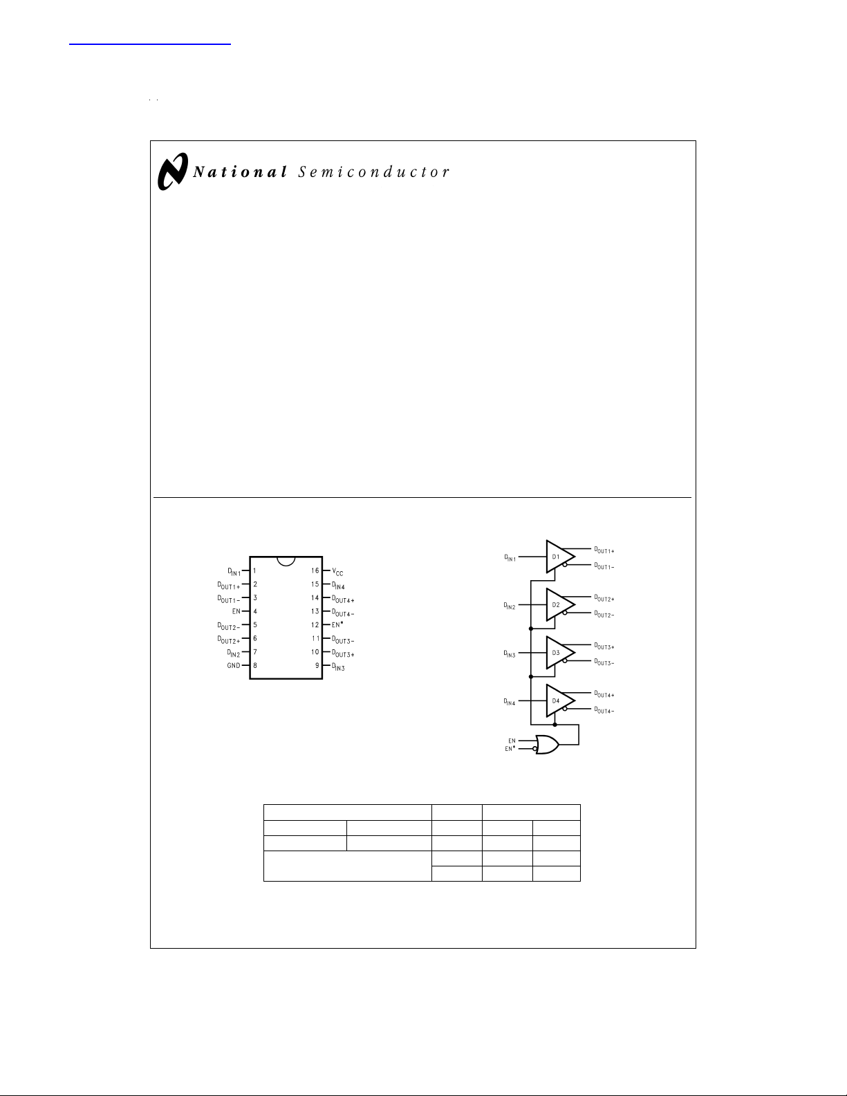
Connection Diagram Functional Diagram
Dual-In-Line
DS100989-1
Order Number
DS90C031BTM,
or DS90C031BTWM
See NS Package Number
M16A or M16B
DS100989-2
Driver Truth Table
Enables Input Outputs
EN EN* D
LHXZZ
All other combinations L L H
of ENABLE inputs H H L
TRI-STATE®is a registered trademark of National Semiconductor Corporation.
© 1999 National Semiconductor Corporation DS100989 www.national.com
D
IN
OUT+
D
OUT−
Absolute Maximum Ratings (Note 1)
If Military/Aerospace specified devices are required,
please contact the National Semiconductor Sales Office/
Distributors for availability and specifications.
Supply Voltage (V
Input Voltage (D
Enable Input Voltage (EN, EN*) −0.3V to (V
Output Voltage (D
Short Circuit Duration
(D
OUT+,DOUT−
Maximum Package Power Dissipation
M Package 1068 mW
WM Package 1562 mW
Derate M Package 8.5 mW/˚C above +25˚C
) −0.3V to +6V
CC
) −0.3V to (VCC+ 0.3V)
IN
OUT+,DOUT−
) −0.3V to +5.8V
CC
+ 0.3V)
) Continuous
@
+25˚C
Lead Temperature Range
Soldering (4 sec.) +260˚C
Maximum Junction
Temperature +150˚C
ESD Rating (Note 7)
(HBM, 1.5 kΩ, 100 pF) ≥ 2kV
(EIAJ, 0 Ω, 200 pF) ≥ 250V
Recommended Operating
Conditions
Min Typ Max Units
Supply Voltage (V
Operating Free Air Temperature (T
DS90C031BT −40 +25 +85 ˚C
) +4.5 +5.0 +5.5 V
CC
)
A
Derate WM Package 12.5 mW/˚C above +25˚C
Storage Temperature Range −65˚C to +150˚C
Electrical Characteristics
Over supply voltage and operating temperature ranges, unless otherwise specified. (Notes 2, 3)
Symbol Parameter Conditions Pin Min Typ Max Units
V
∆V
V
∆V
V
V
V
V
I
V
I
I
I
I
I
I
I
OS
OZ
OFF
CC
CCL
CCZ
Differential Output Voltage RL= 100Ω (
OD1
Change in Magnitude of
OD1
OS
OS
OH
OL
IH
IL
for Complementary
V
OD1
Output States
Offset Voltage 1.10 1.25 1.35 V
Change in Magnitude of
for Complementary
V
OS
Output States
Output Voltage High RL= 100Ω 1.41 1.60 V
Output Voltage Low 0.90 1.07 V
Input Voltage High DIN,
Input Voltage Low GND 0.8 V
Input Current VIN=VCC, GND, 2.5V or 0.4V −10
Input Clamp Voltage ICL= −18 mA −1.5 −0.8 V
CL
Output Short Circuit Current V
OUT
Output TRI-STATE Current EN = 0.8V and EN* = 2.0V,
V
OUT
Power - Off Leakage VO= 0V or 2.4V, VCC= 0V or Open −10
No Load Supply Current
Drivers Enabled
Loaded Supply Current
Drivers Enabled
No Load Supply Current
Drivers Disabled
DIN=VCCor GND V
D
IN
RL= 100Ω (all channels)
V
IN=VCC
DIN=VCCor GND
EN = GND, EN* = V
Figure 1
)D
D
OUT−
OUT+
,
250 345 450 mV
4 35 |mV|
5 25 |mV|
= 0V (Note 8) D
=0VorV
CC
D
EN,
EN*
OUT−
OUT+
,
−10
CC
2.0 V
±
−3.5 −5.0 mA
±
±
1.7 3.0 mA
CC
1 +10 µA
1 +10 µA
1 +10 µA
= 2.5V or 0.4V 4.0 6.5 mA
15.4 21.0 mA
or GND (all inputs)
2.2 4.0 mA
CC
V
Switching Characteristics
VCC= +5.0V, TA= +25˚C (Notes 3, 6, 9)
Symbol Parameter Conditions Min Typ Max Units
t
PHLD
t
PLHD
t
SKD
t
SK1
t
TLH
t
THL
www.national.com 2
Differential Propagation Delay High to Low RL= 100Ω,CL=5pF
Figure 2
Differential Propagation Delay Low to High 1.0 2.1 3.0 ns
Differential Skew |t
PHLD–tPLHD
| 0 80 400 ps
(
Channel-to-Channel Skew (Note 4) 0 300 600 ps
Rise Time 0.35 1.5 ns
Fall Time 0.35 1.5 ns
and
Figure 3
1.0 2.0 3.0 ns
)
Switching Characteristics (Continued)
VCC= +5.0V, TA= +25˚C (Notes 3, 6, 9)
Symbol Parameter Conditions Min Typ Max Units
t
PHZ
t
PLZ
t
PZH
t
PZL
Disable Time High to Z RL= 100Ω,CL=5pF
Figure 4
and
Figure 5
Disable Time Low to Z 2.5 10 ns
(
)
Enable Time Z to High 2.5 10 ns
Enable Time Z to Low 2.5 10 ns
2.5 10 ns
Switching Characteristics
VCC= +5.0V±10%,TA= −40˚C to +85˚C (Notes 3, 6, 9)
Symbol Parameter Conditions Min Typ Max Units
t
PHLD
t
PLHD
t
SKD
t
SK1
t
SK2
t
TLH
t
THL
t
PHZ
t
PLZ
t
PZH
t
PZL
Note 1: “Absolute Maximum Ratings” are those values beyond which the safety of the device cannot be guaranteed. They are not meant to imply that the devices
should be operated at these limits. The table of “Electrical Characteristics” specifies conditions of device operation.
Note 2: Current into device pins is defined as positive. Current out of device pins is defined as negative. All voltages are referenced to ground except: V
∆V
Note 3: All typicals are given for: V
Note 4: Channel-to-Channel Skew is defined as the difference between the propagation delay of the channel and the other channels in the same chip with an event
on the inputs.
Note 5: Chip to Chip Skew is defined as the difference between the minimum and maximum specified differential propagation delays.
Note 6: Generator waveform for all tests unless otherwise specified:f=1MHz, Z
Note 7: ESD Ratings:
Note 8: Output short circuit current (I
Note 9: C
Differential Propagation Delay High to Low RL= 100Ω,CL=5pF
Figure 2
and
Differential Propagation Delay Low to High 0.5 2.1 3.5 ns
Differential Skew |t
PHLD–tPLHD
| 0 80 900 ps
(
Figure 3
Channel-to-Channel Skew (Note 4) 0 0.3 1.0 ns
Chip to Chip Skew (Note 5) 3.0 ns
Rise Time 0.35 2.0 ns
Fall Time 0.35 2.0 ns
Disable Time High to Z RL= 100Ω,CL=5pF
Figure 4
and
Disable Time Low to Z 2.5 15 ns
(
Figure 5
Enable Time Z to High 2.5 15 ns
Enable Time Z to Low 2.5 15 ns
.
OD1
HBM (1.5 kΩ, 100 pF) ≥ 2kV
EIAJ (0Ω, 200 pF) ≥ 250V
includes probe and jig capacitance.
L
= +5.0V, TA= +25˚C.
CC
=50Ω,tr≤6 ns, and tf≤ 6 ns.
O
) is specified as magnitude only, minus sign indicates direction only.
OS
0.5 2.0 3.5 ns
)
2.5 15 ns
)
OD1
and
Parameter Measurement Information
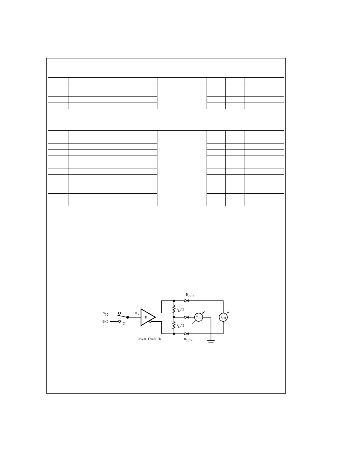
FIGURE 1. Driver VODand VOSTest Circuit
DS100989-3
www.national.com3
Parameter Measurement Information (Continued)
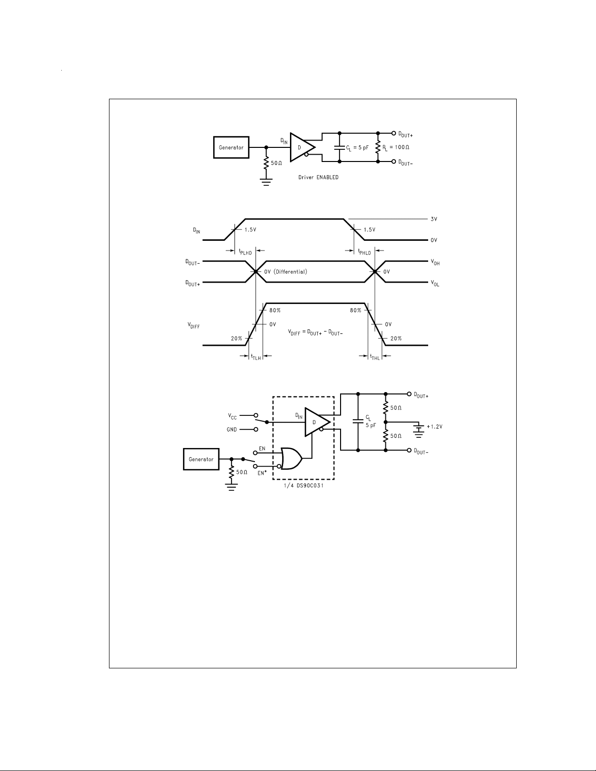
FIGURE 2. Driver Propagation Delay and Transition Time Test Circuit
FIGURE 3. Driver Propagation Delay and Transition Time Waveforms
DS100989-4
DS100989-5
FIGURE 4. Driver TRI-STATE Delay Test Circuit
www.national.com 4
DS100989-6
 Loading...