

查询5962-95833供应商
DS90C031
LVDS Quad CMOS Differential Line Driver
DS90C031 LVDS Quad CMOS Differential Line Driver
June 1998
General Description
The DS90C031 is a quad CMOS differential line driver designed for applications requiring ultra low power dissipation
and high data rates. The device is designed to support data
rates in excess of 155.5 Mbps (77.7 MHz) utilizing Low Voltage Differential Signaling (LVDS) technology.
The DS90C031 accepts TTL/CMOS input levels and translates them to low voltage (350 mV) differential output signals. In addition the driver supports a TRI-STATE
that may be used to disable the output stage, disabling the
load current, andthusdroppingthedevice to an ultra low idle
power state of 11 mW typical.
The DS90C031 and companion line receiver (DS90C032)
provide a new alternative to high power psuedo-ECL devices
for high speed point-to-point interface applications.
®
function
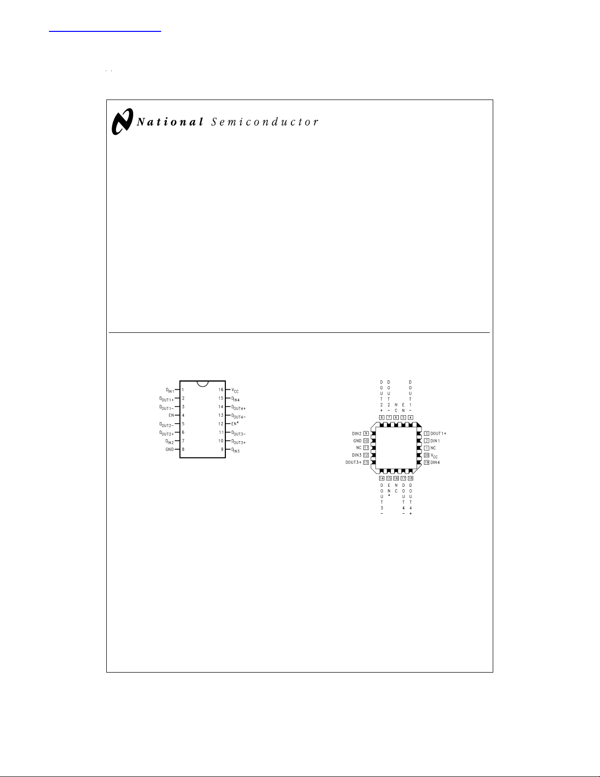
Connection Diagrams
Dual-In-Line
DS011946-1
Order Number DS90C031TM
See NS Package Number M16A
Features
>
n
155.5 Mbps (77.7 MHz) switching rates
±
n
350 mV differential signaling
n Ultra low power dissipation
n 400 ps maximum differential skew (5V, 25˚C)
n 3.5 ns maximum propagation delay
n Industrial operating temperature range
n Military operating temperature range option
n Available in surface mount packaging (SOIC) and (LCC)
n Pin compatible with DS26C31, MB571 (PECL) and
41LG (PECL)
n Compatible with IEEE 1596.3 SCI LVDS standard
n Conforms to ANSI/TIA/EIA-644 LVDS standard
n Available to Standard Microcircuit Drawing (SMD)
5962-95833
LCC Package
DS011946-33
Order Number DS90C031E-QML
See NS Package Number E20A
For Complete Military Specifications,
refer to appropriate SMD or MDS.
TRI-STATE®is a registered trademark of National Semiconductor Corporation.
© 1998 National Semiconductor Corporation DS011946 www.national.com
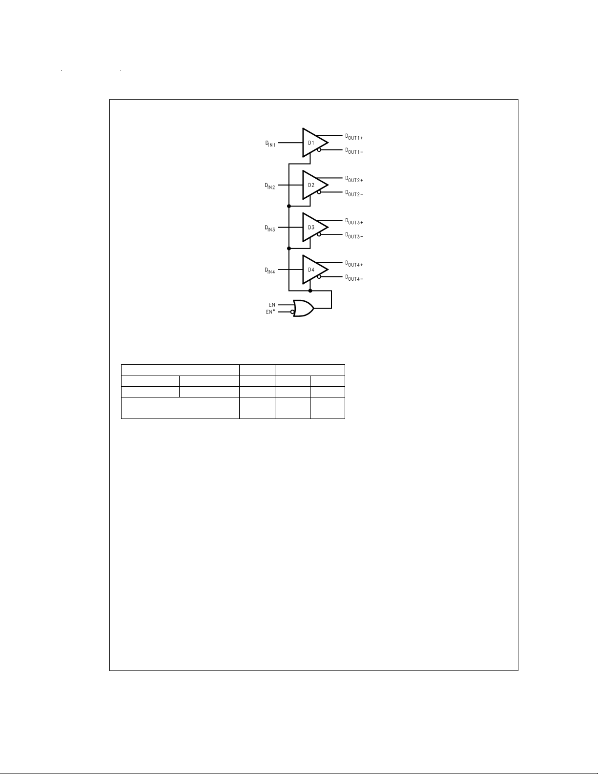
Functional Diagram
Truth Table
DRIVER
Enables Input Outputs
EN EN* D
LHXZZ
All other combinations L L H
of ENABLE inputs H H L
D
IN
OUT+
D
OUT−
DS011946-2
www.national.com 2
Absolute Maximum Ratings (Note 1)
If Military/Aerospace specified devices are required,
please contact the National Semiconductor Sales Office/
Distributors for availability and specifications.
Supply Voltage (V
Input Voltage (D
Enable Input Voltage (EN, EN*) −0.3V to (V
Output Voltage (D
Short Circuit Duration
(D
OUT+,DOUT−
Maximum Package Power Dissipation
M Package 1068 mW
E Package 1900 mW
Derate M Package 8.5 mW/˚C above +25˚C
Derate E Package 12.8 mW/˚C above +25˚C
) −0.3V to +6V
CC
) −0.3V to (VCC+ 0.3V)
IN
OUT+,DOUT−
) −0.3V to (VCC+ 0.3V)
CC
+ 0.3V)
) Continuous
@
+25˚C
Maximum Junction Temperature
(DS90C031T) +150˚C
Maximum Junction Temperature
(DS90C031E) +175˚C
ESD Rating (Note 7)
(HBM, 1.5 kΩ, 100 pF) ≥ 3,500V
(EIAJ, 0 Ω, 200 pF) ≥ 250V
Recommended Operating
Conditions
Min Typ Max Units
Supply Voltage (V
Operating Free Air Temperature (T
DS90C031T −40 +25 +85 ˚C
DS90C031E −55 +25 +125 ˚C
) +4.5 +5.0 +5.5 V
CC
)
A
Storage Temperature Range −65˚C to +150˚C
Lead Temperature Range
Soldering (4 sec.) +260˚C
Electrical Characteristics
Over supply voltage and operating temperature ranges, unless otherwise specified. (Notes 2, 3)
Symbol Parameter Conditions Pin Min Typ Max Units
V
∆V
V
∆V
V
V
V
V
I
V
I
I
I
I
I
Differential Output Voltage RL= 100Ω (
OD1
Change in Magnitude of V
OD1
for Complementary Output
OD1
States
Offset Voltage 1.125 1.25 1.375 V
OS
Change in Magnitude of VOSfor
OS
Complementary Output States
Output Voltage High RL= 100Ω 1.41 1.60 V
OH
Output Voltage Low 0.90 1.07 V
OL
Input Voltage High DIN,
IH
Input Voltage Low GND 0.8 V
IL
Input Current VIN=VCC, GND, 2.5V or 0.4V −10
I
Input Clamp Voltage ICL= −18 mA −1.5 −0.8 V
CL
Output Short Circuit Current V
OS
Output TRI-STATE Current EN = 0.8V and EN* = 2.0V,
OZ
No Load Supply Current
CC
Drivers Enabled
Loaded Supply Current
CCL
Drivers Enabled
No Load Supply Current
CCZ
Drivers Disabled
OUT
V
OUT
DIN=VCCor GND DS90C031T V
D
IN
RL= 100Ω All Channels
V
IN=VCC
(all inputs)
DIN=VCCor GND
EN = GND, EN* = V
Figure 1
)D
D
,
250 345 450 mV
OUT−
OUT+
4 35 |mV|
5 25 |mV|
= 0V (Note 8) D
=0VorV
CC
D
EN,
EN*
OUT−
OUT+
,
CC
2.0 V
−3.5 −5.0 mA
−10
CC
±
1 +10 µA
±
1 +10 µA
1.7 3.0 mA
= 2.5V or 0.4V 4.0 6.5 mA
DS90C031T 15.4 21.0 mA
or GND
DS90C031E 15.4 25.0 mA
DS90C031T 2.2 4.0 mA
CC
DS90C031E 2.2 10.0 mA
V
Switching Characteristics
VCC= +5.0V, TA= +25˚C DS90C031T. (Notes 3, 4, 6, 9)
Symbol Parameter Conditions Min Typ Max Units
t
t
t
t
PHLD
PLHD
SKD
SK1
Differential Propagation Delay High to Low RL= 100Ω,CL=5pF
Figure 2
and
Differential Propagation Delay Low to High 1.0 2.1 3.0 ns
Differential Skew |t
PHLD–tPLHD
| 0 80 400 ps
(
Figure 3
Channel-to-Channel Skew (Note 4) 0 300 600 ps
1.0 2.0 3.0 ns
)
www.national.com3
Switching Characteristics (Continued)
VCC= +5.0V, TA= +25˚C DS90C031T. (Notes 3, 4, 6, 9)
Symbol Parameter Conditions Min Typ Max Units
t
TLH
t
THL
t
PHZ
t
PLZ
t
PZH
t
PZL
Rise Time 0.35 1.5 ns
Fall Time 0.35 1.5 ns
Disable Time High to Z RL= 100Ω,
=5pF
C
Disable Time Low to Z 2.5 10 ns
Enable Time Z to High 2.5 10 ns
L
Figure 4
(
and
Figure 5
)
2.5 10 ns
Enable Time Z to Low 2.5 10 ns
Switching Characteristics
VCC= +5.0V±10%,TA= −40˚C to +85˚C DS90C031T. (Notes 3, 4, 5, 6, 9)
Symbol Parameter Conditions Min Typ Max Units
t
PHLD
t
PLHD
t
SKD
t
SK1
t
SK2
t
TLH
t
THL
t
PHZ
t
PLZ
t
PZH
t
PZL
Differential Propagation Delay High to Low RL= 100Ω,CL=5pF
Figure 2
and
Differential Propagation Delay Low to High 0.5 2.1 3.5 ns
Differential Skew |t
PHLD–tPLHD
| 0 80 900 ps
(
Figure 3
Channel-to-Channel Skew (Note 4) 0 0.3 1.0 ns
Chip to Chip Skew (Note 5) 3.0 ns
Rise Time 0.35 2.0 ns
Fall Time 0.35 2.0 ns
Disable Time High to Z RL= 100Ω,
=5pF
C
Disable Time Low to Z 2.5 15 ns
Enable Time Z to High 2.5 15 ns
L
Figure 4
(
and
Figure 5
Enable Time Z to Low 2.5 15 ns
0.5 2.0 3.5 ns
)
2.5 15 ns
)
Switching Characteristics
VCC= +5.0V±10%,TA= −55˚C to +125˚C DS90C031E. (Notes 3, 4, 5, 6, 9, 10)
Symbol Parameter Conditions Min Typ Max Units
t
PHLD
t
PLHD
t
SKD
t
SK1
t
SK2
t
PHZ
t
PLZ
t
PZH
t
PZL
Differential Propagation Delay High to Low RL= 100Ω,CL=20pF
Figure 3
)
Differential Propagation Delay Low to High 0.5 2.1 5.0 ns
Differential Skew |t
PHLD–tPLHD
| 0 0.08 3.0 ns
Channel-to-Channel Skew (Note 4) 0 0.3 3.0 ns
(
Connected between
C
L
each Output and GND
0.5 2.0 5.0 ns
Chip to Chip Skew (Note 5) 4.5 ns
Disable Time High to Z RL= 100Ω,
=5pF
C
Disable Time Low to Z 2.5 20 ns
Enable Time Z to High 2.5 20 ns
L
Figure 4
(
and
Figure 5
)
2.5 20 ns
Enable Time Z to Low 2.5 20 ns
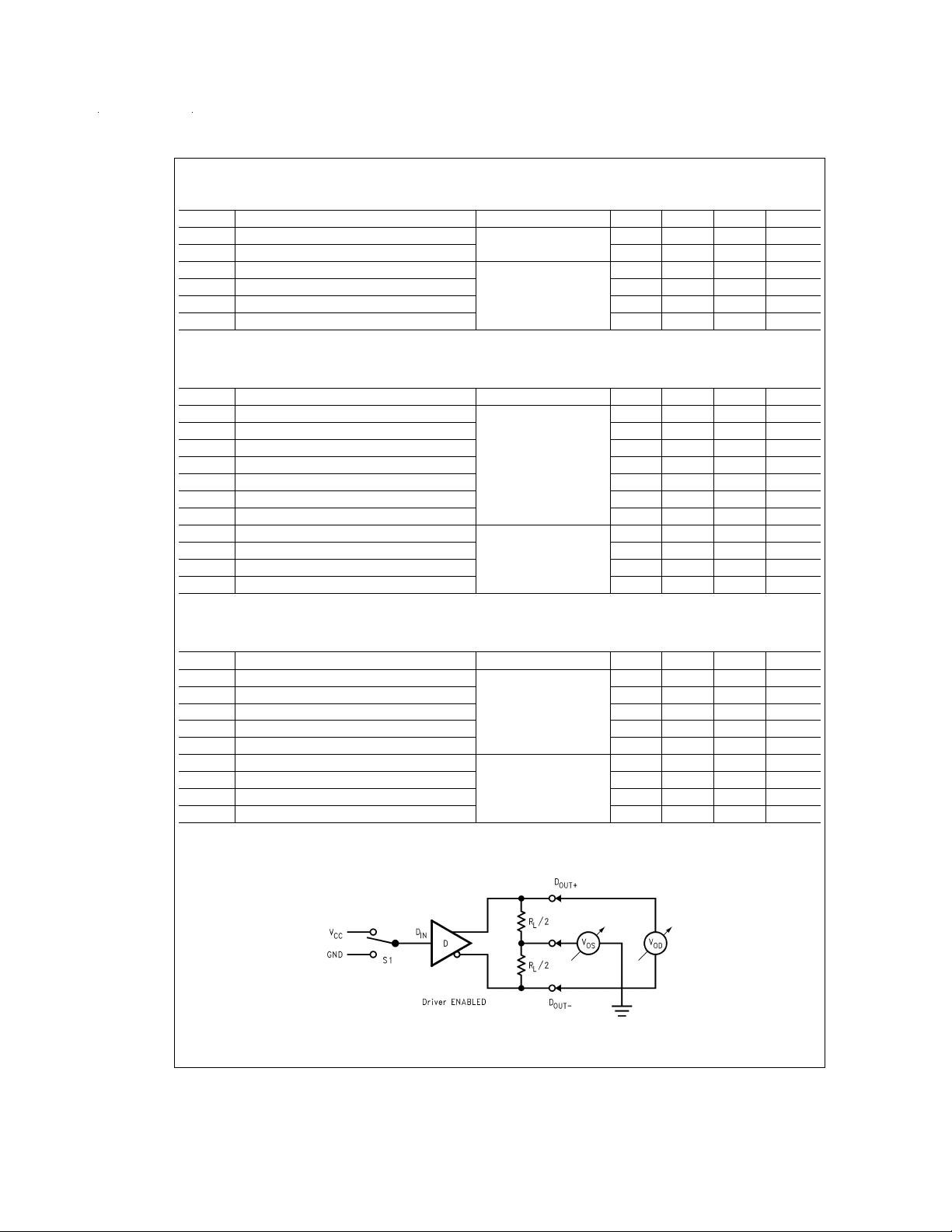
Parameter Measurement Information
FIGURE 1. Driver VODand VOSTest Circuit
www.national.com 4
DS011946-3
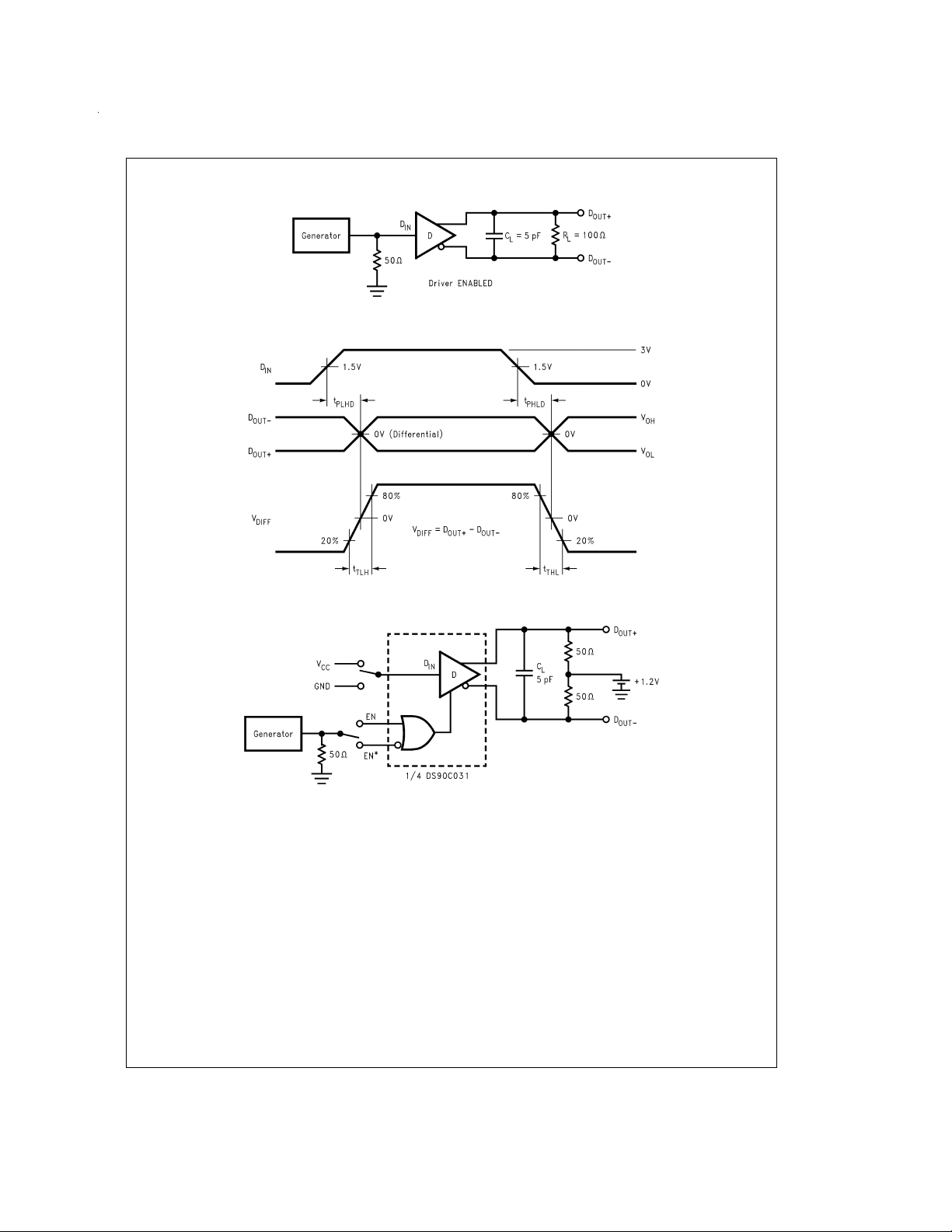
Parameter Measurement Information (Continued)
FIGURE 2. Driver Propagation Delay and Transition Time Test Circuit
FIGURE 3. Driver Propagation Delay and Transition Time Waveforms
DS011946-4
DS011946-5
FIGURE 4. Driver TRI-STATE Delay Test Circuit
DS011946-6
www.national.com5
 Loading...