


DS32EV400
Programmable Quad Equalizer
DS32EV400 Programmable Quad Equalizer
April 18, 2008
General Description
The DS32EV400 programmable quad equalizer provides
compensation for transmission medium losses and reduces
the medium-induced deterministic jitter for four NRZ data
channels. The DS32EV400 is optimized for operation up to
3.2 Gbps for both cables and FR4 traces. Each equalizer
channel has eight levels of input equalization that can be programmed by three control pins, or individually through a Serial
Management Bus (SMBus) interface.
The equalizer supports both AC and DC-coupled data paths
for long run length data patterns such as PRBS-31, and balanced codes such as 8b/10b. The device uses differential
current-mode logic (CML) inputs and outputs. The
DS32EV400 is available in a 7 mm x 7 mm 48-pin leadless
LLP package. Power is supplied from either a 2.5V or 3.3V
supply.
Simplified Application Diagram
Features
Equalizes up to 14 dB loss at 3.2 Gbps
■
8 levels of programmable equalization
■
Settable through control pins or SMBus interface
■
Operates up to 3.2 Gbps with 40” FR4 traces
■
0.12 UI residual deterministic jitter at 3.2 Gbps with 40”
■
FR4 traces
Single 2.5V or 3.3V power supply
■
Signal Detect for individual channels
■
Standby mode for individual channels
■
Supports AC or DC-Coupling with wide input common-
■
mode
Low power consumption: 375 mW Typ at 2.5V
■
Small 7 mm x 7 mm 48-pin LLP package
■
9 kV HBM ESD Rating
■
-40 to 85°C operating temperature range
■
30031924
© 2008 National Semiconductor Corporation 300319 www.national.com

Pin Descriptions
Pin Name Pin # I/O, Type Description
HIGH SPEED DIFFERENTIAL I/O
DS32EV400
IN_0+
IN_0–
IN_1+
IN_1–
IN_2+
IN_2–
IN_3+
IN_3–
OUT_0+
OUT_0–
OUT_1+
OUT_1–
OUT_2+
OUT_2–
OUT_3+
OUT_3–
EQUALIZATION CONTROL
BST_2
BST_1
BST_0
DEVICE CONTROL
EN0 44 I, LVCMOS Enable Equalizer Channel 0 input. When held High, normal operation is selected. When held
EN1 42 I, LVCMOS Enable Equalizer Channel 1 input. When held High, normal operation is selected. When held
EN2 40 I, LVCMOS Enable Equalizer Channel 2 input. When held High, normal operation is selected. When held
EN3 38 I, LVCMOS Enable Equalizer Channel 3 input. When held High, normal operation is selected. When held
FEB 21 I, LVCMOS Force External Boost. When held high, the equalizer boost setting is controlled by BST_[2:0]
SD0 45 O, LVCMOS Equalizer Ch0 Signal Detect Output. Produces a High when signal is detected.
SD1 43 O, LVCMOS Equalizer Ch1 Signal Detect Output. Produces a High when signal is detected.
SD2 41 O, LVCMOS Equalizer Ch2 Signal Detect Output. Produces a High when signal is detected.
SD3 39 O, LVCMOS Equalizer Ch3 Signal Detect Output. Produces a High when signal is detected.
POWER
V
DD
GND 22, 24,
DAP PAD Power Ground reference. The exposed pad at the center of the package must be connected to
1
2
4
5
8
9
11
12
36
35
33
32
29
28
26
25
37
14
23
3, 6, 7,
10, 13,
15, 46
27, 30,
31, 34
I, CML
I, CML
I, CML
I, CML
O, CML
O, CML
O, CML
O, CML
I, LVCMOS BST_2, BST_1, and BST_0 select the equalizer strength for all EQ channels. BST_2 is
Power VDD = 2.5V ± 5% or 3.3V ± 10%. VDD pins should be tied to VDD plane through low inductance
Power Ground reference. GND should be tied to a solid ground plane through a low impedance
Inverting and non-inverting CML differential inputs to the equalizer. An on-chip 100Ω
terminating resistor is connected between IN_0+ and IN_0-. Refer to Figure 6.
Inverting and non-inverting CML differential inputs to the equalizer. An on-chip 100Ω
terminating resistor is connected between IN_1+ and IN_1-. Refer to Figure 6.
Inverting and non-inverting CML differential inputs to the equalizer. An on-chip 100Ω
terminating resistor is connected between IN_2+ and IN_2-. Refer to Figure 6.
Inverting and non-inverting CML differential inputs to the equalizer. An on-chip 100Ω
terminating resistor is connected between IN_3+ and IN_3-. Refer to Figure 6.
Inverting and non-inverting CML differential outputs from the equalizer. An on-chip 50Ω
terminating resistor connects OUT_0+ to VDD and OUT_0- to VDD.
Inverting and non-inverting CML differential outputs from the equalizer. An on-chip 50Ω
terminating resistor connects OUT_1+ to VDD and OUT_1- to VDD.
Inverting and non-inverting CML differential outputs from the equalizer. An on-chip 50Ω
terminating resistor connects OUT_2+ to VDD and OUT_2- to VDD.
Inverting and non-inverting CML differential outputs from the equalizer. An on-chip 50Ω
terminating resistor connects OUT_3+ to VDD and OUT_3- to VDD.
internally pulled high. BST_1 and BST_0 are internally pulled low.
Low, standby mode is selected. EN is internally pulled High.
Low, standby mode is selected. EN is internally pulled High.
Low, standby mode is selected. EN is internally pulled High.
Low, standby mode is selected. EN is internally pulled High.
pins. When held low, the equalizer boost setting is controlled by SMBus (see Table 1) register
bits. FEB is internally pulled High.
path. A 0.01μF bypass capacitor should be connected between each VDD pin to GND planes.
path.
ground plane of the board.
www.national.com 2

Pin Name Pin # I/O, Type Description
SERIAL MANAGEMENT BUS (SMBus) INTERFACE CONTROL PINS
SDA
SDC
CS
Other
Reserv 19, 20
Note: I = Input O = Output
18
17
16
47,48
I/O, LVCMOS
I, LVCMOS
I, LVCMOS
Reserved. Do not connect.
Data input/output (bi-directional). Internally pulled high.
Clock input. Internally pulled high.
Chip select. When pulled high, access to the equalizer SMBus registers are enabled. When
pulled low, access to the equalizer SMBus registers are disabled. Please refer to “SMBus
configuration Registers” section for detail information.
Connection Diagram
DS32EV400
30031926
Ordering Information
NSID Package Type, Qty Size Package ID
DS32EV400SQ 48–pin LLP (7 mm x 7 mm x 0.8 mm, 0.5 mm pitch, reel of 250 SQA48D
DS32EV400SQX 48–pin LLP (7 mm x 7 mm x 0.8 mm, 0.5 mm pitch, reel of 2500 SQA48D
3 www.national.com
Absolute Maximum Ratings (Note 1)
If Military/Aerospace specified devices are required,
please contact the National Semiconductor Sales Office/
Distributors for availability and specifications.
DS32EV400
Supply Voltage (VDD)
CMOS Input Voltage -0.5V + 4.0V
CMOS Output Voltage -0.5V to 4.0V
CML Input/Output Voltage -0.5V to 4.0V
Junction temperature +150°C
Storage temperature -65°C to +150°C
Lead temperature (Soldering, 4
Seconds)
-0.5V to +4.0V
+260°C
ESD rating
HBM, 1.5 kΩ, 100 pF
EIAJ, 0Ω, 200pF
Thermal Resistance
θJA, no airflow
Recommended Operating Conditions
Min Typ Max Units
Supply Voltage (Note 9)
V
to GND 2.375 2.5 2.625 V
DD2.5
V
to GND 3.0 3.3 3.6 V
DD3.3
Ambient Temperature -40 25 +85 °C
Electrical Characteristics
Over recommended operating supply and temperature ranges with default register settings unless other specified.
Symbol Parameter Conditions Min
POWER
P Power Supply Consumption Device Output Enabled
(EN [0–3] = High), V
DD3.3
Device Output Disable
(EN [0–3] = Low), V
DD3.3
P Power Supply Consumption Device Output Enabled
(EN [0–3] = High), V
DD2.5
Device Output Disable
(EN [0–3] = Low), V
DD2.5
N Supply Noise Tolerance (Note 4) 50 Hz — 100 Hz
100 Hz — 10 MHz
10 MHz — 1.6 GHz
LVCMOS DC SPECIFICATIONS
V
IH
V
IL
V
OH
V
OL
I
IN
High Level Input Voltage V
V
DD3.3
DD2.5
Low Level Input Voltage -0.3 0.8 V
High Level Output Voltage IOH = -3mA, V
IOH = -3mA, V
DD3.3
DD2.5
Low Level Output Voltage IOL = 3mA 0.4 V
Input Leakage Current VIN = V
DD
VIN = GND -15
I
IN-P
Input Leakage Current with
Internal Pull-Down/Up Resistors
VIN = VDD, with internal pull-down
resistors
VIN = GND, with internal pull-up
resistors
SIGNAL DETECT
SDH Signal Detect ON Threshold Level Default input signal level to assert
SD pin, 3.2 Gbps
SDI Signal Detect OFF Threshold
Level
Default input signal level to deassert SD, 3.2Gbps
2.0
1.6
2.4 V
2.0
+15
+120
-20
70 mV
40 mV
Typ
(note 2)
490 700 mW
360 490 mW
100
> 9 kV
> 250 V
30°C/W
Max Units
100 mW
30
mV
40
10
V
V
DD3.3
DD2.5
mV
mV
P-P
P-P
P-P
V
V
μA
μA
μA
μA
p-p
p-p
www.national.com 4
DS32EV400
Symbol Parameter Conditions Min
Typ
(note 2)
Max Units
CML RECEIVER INPUTS (IN_n+, IN_n-)
V
TX
Source Transmit Launch Signal
Level (IN diff)
AC-Coupled or DC-Coupled
Requirement, Differential
measurement at point A.
400 1600
mV
P-P
Figure 1
V
INTRE
V
DDTX
V
ICMDC
R
LI
R
IN
Input Threshold Voltage Differential measurement at
point B. Figure 1
Supply Voltage of Transmitter toEQDC-Coupled Requirement
(Note 10)
Input Common Mode Voltage DC-Coupled Requirement,
Differential measurement at point
A. Figure 1, (Note 7)
Differential Input Return Loss 100MHz – 1.6GHz, with fixture’s
effect de-embedded
Input Resistance Differential across IN+ and IN-,
Figure 6.
120
V
V
DD
DDTX
0.2
–
1.6
V
–
DDTX
0.8
10 dB
85 100 115
mV
P-P
V
V
Ω
CML OUTPUTS (OUT_n+, OUT_n-)
V
OD
Output Differential Voltage Level
(OUT diff)
Differential measurement with
OUT+ and OUT- terminated by
50Ω to GND, AC-Coupled
500 620 725
mV
P-P
Figure 2
V
OCM
Output Common Mode Voltage Single-ended measurement DC-
Coupled with 50Ω terminations
VDD– 0.2
VDD– 0.1
V
(Note 7)
tR, t
F
Transition Time 20% to 80% of differential output
voltage, measured within 1” from
20 60 ps
output pins. Figure 2, (Note 7)
R
O
R
LO
Output Resistance Single ended to V
DD
Differential Output Return Loss 100 MHz – 1.6 GHz, with fixture’s
effect de-embedded. IN+ = static
42 50 58
10 dB
Ω
high.
t
PLHD
t
PHLD
t
CCSK
t
PPSK
Differential Low to High
Propagation Delay
Differential High to Low
Propagation Delay
Inter Pair Channel to Channel
Skew
Propagation delay measurement
at 50% VO between input to
output, 100 Mbps. Figure 3,
(Note 7)
Difference in 50% crossing
between channels
Part to Part Output Skew Difference in 50% crossing
between outputs
240 ps
240 ps
7 ps
20 ps
EQUALIZATION
DJ1 Residual Deterministic Jitter
at 3.2 Gbps
40” of 6 mil microstrip FR4,
EQ Setting 0x07, PRBS-7 (27-1)
0.12 0.20
UI
P-P
pattern. (Note 5, 6)
DJ2 Residual Deterministic Jitter
at 2.5 Gbps
40” of 6 mil microstrip FR4,
EQ Setting 0x07, PRBS-7 (27-1)
0.1 0.16
UI
P-P
pattern. (Note 5, 6)
DJ3 Residual Deterministic Jitter
at 1 Gbps
40” of 6 mil microstrip FR4,
EQ Setting 0x07, PRBS-7 (27-1)
0.05
UI
P-P
pattern. (Note 5, 6)
RJ Random Jitter (Note 7, 8) 0.5 psrms
5 www.national.com
Symbol Parameter Conditions Min
Typ
(note 2)
Max Units
SIGNAL DETECT and ENABLE TIMING
t
DS32EV400
ZISD
t
IZSD
Input OFF to ON detect — SD
Output High Response Time
Input ON to OFF detect — SD
Output Low Response Time
Response time measurement at
VIN to SD output, VIN = 800 mV
100 Mbps, 40” of 6 mil microstrip
FR4
P-P
35 ns
,
400 ns
(Figure 1, 4), (Note 7)
t
OZOED
t
ZOED
EN High to Output ON Response
Time
EN Low to Output OFF Response
Time
Response time measurement at
EN input to VO, VIN = 800 mV
P-P
100 Mbps, 40” of 6 mil microstrip
FR4
,
150 ns
5 ns
(Figure 1, 5), (Note 7)
Note 1: “Absolute Maximum Ratings” indicate limits beyond which damage to the device may occur, including inoperability and degradation of device reliability
and/or performance. Functional operation of the device and/or non-degradation at the Absolute Maximum Ratings or other conditions beyond those indicated in
the Recommended Operating Conditions is not implied. The Recommended Operating Conditions indicate conditions at which the device is functional and the
device should not be operated beyond such conditions. Absolute Maximum Numbers are guaranteed for a junction temperature range of –40°C to +125°C. Models
are validated to Maximum Operating Voltages only.
Note 2: Typical values represent most likely parametric norms at VDD = 3.3V, TA = 25°C, and at the Recommended Operation Conditions at the time of product
characterization and are not guaranteed.
Note 3: The Electrical Characteristics tables list guaranteed specifications under the listed Recommended Operating Conditions except as otherwise modified
or specified by the Electrical Characteristics Conditions and/or Notes. Typical specifications are estimations only and are not guaranteed.
Note 4: Allowed supply noise (mV
Note 5: Specification is guaranteed by characterization and is not tested in production.
Note 6: Deterministic jitter is measured at the differential outputs (point C of Figure 1), minus the deterministic jitter before the test channel (point A of Figure 1).
Random jitter is removed through the use of averaging or similar means.
Note 7: Measured with clock like {11111 00000} pattern.
Note 8: Random jitter contributed by the equalizer is defined as sqrt (J
Figure 1; JIN is the random jitter at the input of the equalizer in ps-rms, see Figure 1.
Note 9: The V
is VDD = 2.5V ± 5% and V
DD2.5
sine wave) under typical conditions.
P-P
is VDD = 3.3V ± 10%.
DD3.3
OUT
2
− J
2
). J
is the random jitter at the equalizer outputs in ps-rms, see point C of
IN
OUT
www.national.com 6

Electrical Characteristics — Serial Management Bus Interface
Over recommended operating supply and temperature ranges unless other specified.
Symbol Parameter Conditions Min Typ Max Units
SERIAL BUS INTERFACE DC SPECIFICATIONS
V
IL
Data, Clock Input Low Voltage

System Management Bus (SMBus) and Configuration Registers
The System Management Bus interface is compatible to SM-
DS32EV400
Bus 2.0 physical layer specification. The use of the Chip
Select signal is required. Holding the CS pin High enables
the SMBus port allowing access to the configuration registers.
Holding the CS pin Low disables the device's SMBus allowing
communication from the host to other slave devices on the
bus. In the STANDBY state, the System Management Bus
remains active. When communication to other devices on the
SMBus is active, the CS signal for the DS32EV400s must be
driven Low.
The address byte for all DS32EV400s is AC'h. Based on the
SMBus 2.0 specification, the DS32EV400 has a 7-bit slave
address of 1010110'b. The LSB is set to 0'b (for a WRITE),
thus the 8-bit value is 1010 1100'b or AC'h.
The SDC and SDA pins are 3.3V LVCMOS signaling and include high-Z internal pull up resistors. External low
impedance pull up resistors maybe required depending upon
SMBus loading and speed. Note, these pins are not 5V tolerant.
Transfer of Data via the SMBus
During normal operation the data on SDA must be stable during the time when SDC is High.
There are three unique states for the SMBus:
START: A High-to-Low transition on SDA while SDC is High
indicates a message START condition.
STOP: A Low-to-High transition on SDA while SDC is High
indicates a message STOP condition.
IDLE: If SDC and SDA are both High for a time exceeding
t
from the last detected STOP condition or if they are High
BUF
for a total exceeding the maximum specification for t
the bus will transfer to the IDLE state.
HIGH
then
SMBus Transactions
The device supports WRITE and READ transactions. See
Register Description table for register address, type (Read/
Write, Read Only), default value and function information.
Writing a Register
To write a register, the following protocol is used (see SMBus
2.0 specification).
1.
The Host (Master) selects the device by driving its
SMBus Chip Select (CS) signal High.
2.
The Host drives a START condition, the 7-bit SMBus
address, and a “0” indicating a WRITE.
3.
The Device (Slave) drives the ACK bit (“0”).
4.
The Host drives the 8-bit Register Address.
5.
The Device drives an ACK bit (“0”).
6.
The Host drive the 8-bit data byte.
7.
The Device drives an ACK bit (“0”).
8.
The Host drives a STOP condition.
9.
The Host de-selects the device by driving its SMBus CS
signal Low.
The WRITE transaction is completed, the bus goes IDLE and
communication with other SMBus devices may now occur.
Reading a Register
To read a register, the following protocol is used (see SMBus
2.0 specification).
1.
The Host (Master) selects the device by driving its
SMBus Chip Select (CS) signal High.
2.
The Host drives a START condition, the 7-bit SMBus
address, and a “0” indicating a WRITE.
3.
The Device (Slave) drives the ACK bit (“0”).
4.
The Host drives the 8-bit Register Address.
5.
The Device drives an ACK bit (“0”).
6.
The Host drives a START condition.
7.
The Host drives the 7-bit SMBus Address, and a “1”
indicating a READ.
8.
The Device drives an ACK bit “0”.
9.
The Device drives the 8-bit data value (register contents).
10.
The Host drives a NACK bit “1”indicating end of the
READ transfer.
11.
The Host drives a STOP condition.
12.
The Host de-selects the device by driving its SMBus CS
signal Low.
The READ transaction is completed, the bus goes IDLE and
communication with other SMBus devices may now occur.
Please see Table 1 for more information.
www.national.com 8

TABLE 1. SMBus Register Address
Name Address Default Type Bit 7 Bit 6 Bit 5 Bit 4 Bit 3 Bit 2 Bit 1 Bit 0
Status 0x00 0x00 RO ID Revision SD3 SD2 SD1 SD0
Status 0x01 0x00 RO EN1 Boost 1 EN0 Boost 0
Status 0x02 0x00 RO EN3 Boost 3 EN2 Boost 2
Enable/
Boost
(CH 0, 1)
Enable/
Boost
(CH 2, 3)
Signal
Detect
Signal
Detect
SMBus
Control
0x03 0x44 RW EN1 Output
0:Enable
1:Disable
0x04 0x44 RW EN3 Output
0:Enable
1:Disable
0x05 0x00 RW SD3 ON Threshold
Select
00: 70 mV (Default)
01: 55 mV
10: 90 mV
11: 75 mV
0x06 0x00 RW SD3 OFF Threshold
Select
00: 40 mV (Default)
01: 30 mV
10: 55 mV
11: 45 mV
Boost Control for CH1
000 (Min Boost)
001
010
011
100 (Default)
101
110
111 (Max Boost)
Boost Control for CH3
000 (Min Boost)
001
010
011
100 (Default)
101
110
111 (Max Boost)
SD2 ON Threshold
Select
00: 70 mV (Default)
01: 55 mV
10: 90 mV
11: 75 mV
SD2 OFF Threshold
Select
00: 40 mV (Default)
01: 30 mV
10: 55 mV
11: 45 mV
EN0 Output
0:Enable
1:Disable
Boost Control for CH0
000 (Min Boost)
001
010
011
100 (Default)
101
110
111 (Max Boost)
EN2 Output
0:Enable
1:Disable
Boost Control for CH2
000 (Min Boost)
001
010
011
100 (Default)
101
110
111 (Max Boost)
SD1 ON Threshold
Select
00: 70 mV (Default)
01: 55 mV
10: 90 mV
11: 75 mV
SD1 OFF Threshold
Select
00: 40 mV (Default)
01: 30 mV
10: 55 mV
11: 45 mV
SD0 ON Threshold
Select
00: 70 mV (Default)
01: 55 mV
10: 90 mV
11: 75 mV
SD0 OFF Threshold
Select
00: 40 mV (Default)
01: 30 mV
10: 55 mV
11: 45 mV
0x07 0x00 RW Reserved SMBus
Enable
Control
0: Disable
1: Enable
Output
Level
0x08 0x78 RW Reserved Output Level:
00: 400 mV
01: 540 mV
10: 620 mV
Reserved
P-P
P-P
P-P
(Default)
11: 760 mV
Note: RO = Read Only, RW = Read/Write
P-P
DS32EV400
9 www.national.com

DS32EV400
30031927
FIGURE 1. Test Setup Diagram
30031937
FIGURE 2. CML Output Transition Times
FIGURE 3. Propagation Delay Timing Diagram
FIGURE 4. Signal Detect (SD) Delay Timing Diagram
www.national.com 10
30031901
30031902

FIGURE 5. Enable (EN) Delay Timing Diagram
DS32EV400
30031903
30031907
FIGURE 6. Simplified Receiver Input Termination Circuit
FIGURE 7. SMBus Timing Parameters
30031906
11 www.national.com
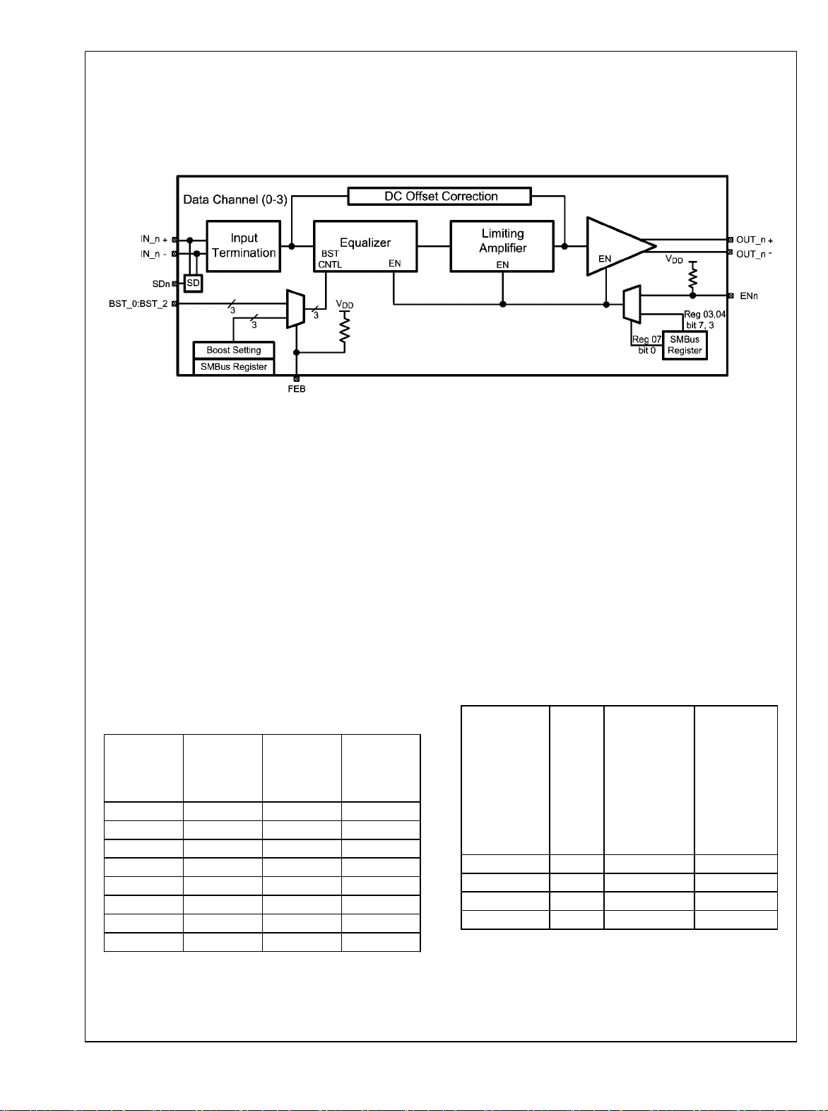
DS32EV400 Functional Descriptions
The DS32EV400 is a programmable quad equalizer opti-
DS32EV400
mized for operation up to 3.2 Gbps for backplane and cable
applications.
FIGURE 8. Simplified Block Diagram
DATA CHANNELS
The DS32EV400 provides four data channels. Each data
channel consists of an equalizer stage, a limiting amplifier, a
DC offset correction block, and a CML driver as shown in Figure 8.
30031904
EQUALIZER BOOST CONTROL
Each data channel supports eight programmable levels of
equalization boost. The state of the FEB pin determines how
the boost settings are controlled. If the FEB pin is held High,
then the equalizer boost setting is controlled by the Boost Set
pins (BST_[2:0]) in accordance with Table 2. If this programming method is chosen, then the boost setting selected on the
Boost Set pins is applied to all channels. When the FEB pin
is held Low, the equalizer boost level is controlled through the
SMBus. This programming method is accessed via the appropriate SMBus registers (see Table 1). Using this approach,
equalizer boost settings can be programmed for each channel
individually. FEB is internally pulled High (default setting);
therefore if left unconnected, the boost settings are controlled
by the Boost Set pins (BST_[2:0]). The eight levels of boost
settings enables the DS32EV400 to address a wide range of
media loss and data rates.
TABLE 2. EQ Boost Control Table
6 mil
microstrip
FR4 trace
length (in)
0 0 0 0 0 0
5 2 3 0 0 1
10 3 6 0 1 0
15 4 7 0 1 1
20 5 8 1 0 0 (Default)
25 6 10 1 0 1
30 7 12 1 1 0
40 10 14 1 1 1
24 AWG
Twin-AX
cable length
(m)
Channel
Loss at 1.6
GHz (dB)
BST_N
[2, 1, 0]
DEVICE STATE AND ENABLE CONTROL
The DS32EV400 has an enable feature on each data channel
which provides the ability to control device power consumption. This feature can be controlled either an Enable Pin
(EN_n) with Reg 07 = 00'h (default value), or by the Enable
Control Bit register which can be configured through the SMBus port (see Table 1 and Table 3 for detail register information), which require setting Reg 07 = 01'h and changing
register value of Reg 03, 04. If the Enable is activated using
either the external EN_n pin or SMBUS register, the corresponding data channel is placed in the ACTIVE state and all
device blocks function as described. The DS32EV400 can also be placed in STANDBY mode to save power. In the
STANDBY mode only the control interface including the SMBus port, as well as the signal detection circuit remain active.
TABLE 3. Controlling Device State
Reg. 07 bit 0 EN Pin
(CMOS)
0 : Disable 1 X ACTIVE
0 : Disable 0 X STANDBY
1 : Enable X 0 ACTIVE
1 : Enable X 1 STANDBY
CH 0:
Reg. 03 bit 3
CH 1:
Reg. 03 bit 7
CH 2:
Reg. 04 bit 3
CH 3:
Reg. 04 bit 7
(EN Control)
Device State
www.national.com 12

DS32EV400
SIGNAL DETECT
The DS32EV400 features a signal detect circuit on each data
channel. The status of the signal of each channel can be determined by either reading the Signal Detect bit (SDn) in the
SMBus registers (see Table 1) or by the state of each SDn
pin. An output logic high indicates the presence of a signal
that has exceeded the ON threshold value (called SD_ON).
An output logic Low means that the input signal has fallen
below the OFF threshold value (called SD_OFF). These values are programmed via the SMBus (Table 1). If not programmed via the SMBus, the thresholds take on the default
values as shown in Table 4. The Signal Detect threshold values can be changed through the SMBus. All threshold values
specified are DC peak-to-peak differential signals (positive
signal minus negative signal) at the input of the device.
TABLE 4. Signal Detect Threshold Values
Channel 0:
Bit 1
Channel 1:
Bit 3
Channel2:
Bit 5
Channel 3:
Bit 7
Channel 0:
Bit 0
Channel 1:
Bit 2
Channel2:
Bit 4
Channel 3:
Bit 6
SD_OFF
Threshold
Register 06
(mV)
SD_ON
Threshold
Register 05
(mV)
0 0 40 (Default) 70 (Default)
0 1 30 55
1 0 55 90
1 1 45 75
level is 620 mVp-p. The following Table presents the output
level values supported:
TABLE 5. Output Level Control Settings
All Channels: Bit 3 All Channels: Bit 2 Output Level
Register 08
(mV
)
P-P
0 0 400
0 1 540
1 0 620 (Default)
1 1 760
AUTOMATIC ENABLE FEATURE
It may be desirable to place unused channels in power-saving
Standby mode. This can be accomplished by connecting the
Signal detect (SDn) pin to the Enable (ENn) pin for each
channel (See Figure 9). In order for this option to function
properly, the register value for Reg. 07 should be 00'h (default
value). If an input signal swing applied to a data channel is
above the voltage level threshold as shown in Table 4, then
the SDn output pin is asserted High. If the SDn pin is connected to the ENn pin, this will enable the equalizer, limiting
amplifier, and output buffer on the data channels; thus the
DS32EV400 will automatically enter the ACTIVE state. If the
input signal swing falls below the SD_OFF threshold level,
then the SDn output will be asserted Low, causing the channel
to be placed in the STANDBY state.
OUTPUT LEVEL CONTROL
The output amplitude of the CML drivers for each channel can
be controlled via the SMBus (see Table 1). The default output
13 www.national.com

DS32EV400 Applications Information
DS32EV400
30031905
FIGURE 9. Automatic Enable Configuration
UNUSED EQUALIZER CHANNELS
It is recommended to put all unused channels into standby
mode.
GENERAL RECOMMENDATIONS
The DS32EV400 is a high performance circuit capable of delivering excellent performance. Careful attention must be paid
to the details associated with high-speed design as well as
providing a clean power supply. Refer to the LVDS Owner's
Manual for more detailed information on high speed design
tips to address signal integrity design issues.
PCB LAYOUT CONSIDERATIONS FOR DIFFERENTIAL PAIRS
The CML inputs and outputs must have a controlled differential impedance of 100Ω. It is preferable to route CML lines
exclusively on one layer of the board, particularly for the input
traces. The use of vias should be avoided if possible. If vias
must be used, they should be used sparingly and must be
placed symmetrically for each side of a given differential pair.
Route the CML signals away from other signals and noise
sources on the printed circuit board. See AN-1187 for additional information on LLP packages.
POWER SUPPLY BYPASSING
Two approaches are recommended to ensure that the
DS32EV400 is provided with an adequate power supply.
First, the supply (VDD) and ground (GND) pins should be connected to power planes routed on adjacent layers of the
printed circuit board. The layer thickness of the dielectric
should be minimized so that the VDD and GND planes create
a low inductance supply with distributed capacitance. Second, careful attention to supply bypassing through the proper
use of bypass capacitors is required. A 0.01μF bypass capacitor should be connected to each VDD pin such that the
capacitor is placed as close as possible to the DS32EV400.
Smaller body size capacitors can help facilitate proper component placement. Additionally, three capacitors with capacitance in the range of 2.2 μF to 10 μF should be incorporated
in the power supply bypassing design as well. These capacitors can be either tantalum or an ultra-low ESR ceramic and
should be placed as close as possible to the DS32EV400.
DC COUPLING
The DS32EV400 supports both AC coupling with external ac
coupling capacitor, and DC coupling to its upstream driver, or
downstream receiver. With DC coupling, users must ensure
the input signal common mode is within the range of the electrical specification V
with 50 Ω to VDD.
and the device output is terminated
ICMDC
www.national.com 14

Typical Performance Eye Diagrams and Curves
DS32EV400
Figure 8. Equalized Signal
30031908
(40 In FR4, 1 Gbps, PRBS7, 0x07 Setting)
Figure 10. Equalized Signal
30031910
(40 In FR4, 3.2Gbps, PRBS7, 0x07 Setting)
Figure 9. Equalized Signal
30031909
(40 In FR4, 2.5Gbps, PRBS7, 0x07 Setting)
Figure 11. Equalized Signal
30031911
(10m 24 AWG Twin-AX Cable, 3.2 Gbps, PRBS7, 0x07 Setting)
Figure 12. Equalized Signal
30031912
(32 In Tyco XAUI Backplane, 3.125 Gbps, PRBS7, 0x07
Setting)
Figure 13. DJ vs. EQ Setting (3.2 Gbps)
15 www.national.com
30031913

Physical Dimensions inches (millimeters) unless otherwise noted
DS32EV400
48-pin LLP Package (7 mm x 7 mm x 0.8 mm, 0.5 mm pitch)
Order Number DS32EV400SQ
Package Number SQA48D
www.national.com 16

Notes
DS32EV400
17 www.national.com
Notes
For more National Semiconductor product information and proven design tools, visit the following Web sites at:
Products Design Support
Amplifiers www.national.com/amplifiers WEBENCH www.national.com/webench
Audio www.national.com/audio Analog University www.national.com/AU
Clock Conditioners www.national.com/timing App Notes www.national.com/appnotes
Data Converters www.national.com/adc Distributors www.national.com/contacts
Displays www.national.com/displays Green Compliance www.national.com/quality/green
Ethernet www.national.com/ethernet Packaging www.national.com/packaging
Interface www.national.com/interface Quality and Reliability www.national.com/quality
LVDS www.national.com/lvds Reference Designs www.national.com/refdesigns
Power Management www.national.com/power Feedback www.national.com/feedback
Switching Regulators www.national.com/switchers
LDOs www.national.com/ldo
LED Lighting www.national.com/led
PowerWise www.national.com/powerwise
Serial Digital Interface (SDI) www.national.com/sdi
Temperature Sensors www.national.com/tempsensors
DS32EV400 Programmable Quad Equalizer
Wireless (PLL/VCO) www.national.com/wireless
THE CONTENTS OF THIS DOCUMENT ARE PROVIDED IN CONNECTION WITH NATIONAL SEMICONDUCTOR CORPORATION
(“NATIONAL”) PRODUCTS. NATIONAL MAKES NO REPRESENTATIONS OR WARRANTIES WITH RESPECT TO THE ACCURACY
OR COMPLETENESS OF THE CONTENTS OF THIS PUBLICATION AND RESERVES THE RIGHT TO MAKE CHANGES TO
SPECIFICATIONS AND PRODUCT DESCRIPTIONS AT ANY TIME WITHOUT NOTICE. NO LICENSE, WHETHER EXPRESS,
IMPLIED, ARISING BY ESTOPPEL OR OTHERWISE, TO ANY INTELLECTUAL PROPERTY RIGHTS IS GRANTED BY THIS
DOCUMENT.
TESTING AND OTHER QUALITY CONTROLS ARE USED TO THE EXTENT NATIONAL DEEMS NECESSARY TO SUPPORT
NATIONAL’S PRODUCT WARRANTY. EXCEPT WHERE MANDATED BY GOVERNMENT REQUIREMENTS, TESTING OF ALL
PARAMETERS OF EACH PRODUCT IS NOT NECESSARILY PERFORMED. NATIONAL ASSUMES NO LIABILITY FOR
APPLICATIONS ASSISTANCE OR BUYER PRODUCT DESIGN. BUYERS ARE RESPONSIBLE FOR THEIR PRODUCTS AND
APPLICATIONS USING NATIONAL COMPONENTS. PRIOR TO USING OR DISTRIBUTING ANY PRODUCTS THAT INCLUDE
NATIONAL COMPONENTS, BUYERS SHOULD PROVIDE ADEQUATE DESIGN, TESTING AND OPERATING SAFEGUARDS.
EXCEPT AS PROVIDED IN NATIONAL’S TERMS AND CONDITIONS OF SALE FOR SUCH PRODUCTS, NATIONAL ASSUMES NO
LIABILITY WHATSOEVER, AND NATIONAL DISCLAIMS ANY EXPRESS OR IMPLIED WARRANTY RELATING TO THE SALE
AND/OR USE OF NATIONAL PRODUCTS INCLUDING LIABILITY OR WARRANTIES RELATING TO FITNESS FOR A PARTICULAR
PURPOSE, MERCHANTABILITY, OR INFRINGEMENT OF ANY PATENT, COPYRIGHT OR OTHER INTELLECTUAL PROPERTY
RIGHT.
LIFE SUPPORT POLICY
NATIONAL’S PRODUCTS ARE NOT AUTHORIZED FOR USE AS CRITICAL COMPONENTS IN LIFE SUPPORT DEVICES OR
SYSTEMS WITHOUT THE EXPRESS PRIOR WRITTEN APPROVAL OF THE CHIEF EXECUTIVE OFFICER AND GENERAL
COUNSEL OF NATIONAL SEMICONDUCTOR CORPORATION. As used herein:
Life support devices or systems are devices which (a) are intended for surgical implant into the body, or (b) support or sustain life and
whose failure to perform when properly used in accordance with instructions for use provided in the labeling can be reasonably expected
to result in a significant injury to the user. A critical component is any component in a life support device or system whose failure to perform
can be reasonably expected to cause the failure of the life support device or system or to affect its safety or effectiveness.
National Semiconductor and the National Semiconductor logo are registered trademarks of National Semiconductor Corporation. All other
brand or product names may be trademarks or registered trademarks of their respective holders.
Copyright© 2008 National Semiconductor Corporation
For the most current product information visit us at www.national.com
www.national.com
National Semiconductor
Americas Technical
Support Center
Email:
new.feedback@nsc.com
Tel: 1-800-272-9959
National Semiconductor Europe
Technical Support Center
Email: europe.support@nsc.com
German Tel: +49 (0) 180 5010 771
English Tel: +44 (0) 870 850 4288
National Semiconductor Asia
Pacific Technical Support Center
Email: ap.support@nsc.com
National Semiconductor Japan
Technical Support Center
Email: jpn.feedback@nsc.com
 Loading...