

Page 1

3.125 Gbps 4x4 LVDS Crosspoint Switch
with Transmit Pre-emphasis
and Receive Equalization
DS25CP104 Evaluation Kit
USER MANUAL
Part Number: DS25CP104EVK
For the latest documents concerning these products and evaluation kit, visit lvds.national.com.
Schematics and gerber files are also available at lvds.national.com.
February 2008
Rev. 0.2
Page 2

DS25CP104EVK User Manual
Table of Contents
Table of Contents…..........................................................................................................2
Overview………………………………………………………………………………...3
DS25CP104 EVK Description …………………………………………………………4
CP104 Evaluation ………………………………………………………………………6
SMBus Evaluation ……………………………………………………………………..12
Typical Performance …………………………………………………………………...16
Page 2 of 17
Page 3
DS25CP104EVK User Manual
Overview
The DS25CP104EVK is an evaluation kit designed for demonstrating performance of
DS25CP104, a 3.125 Gbps 4x4 LVDS Crosspoint Switch with Transmit Pre-emphasis
and Receive Equalization. The evaluation kit is comprised of the DS25CP104 with its
associated input and output SMA connectors and jumpers to manually select the desired
pre-emphasis or equalization, a USB to SMBus conversion circuit to control the SMBus
with a PC, and three FR4 striplines (15” (38.1cm), 30” (76.2cm), and 60” (152.4cm) ) to
exercise the devices’ signal conditioning features (pre-emphasis and equalization).
The purpose of this document is to familiarize the user with the DS25CP104EVK, to
suggest test setup procedures and instrumentation to test the device optimally, and to
guide the user through some typical measurements that demonstrate the performance of
the DS25CP104 in typical applications.
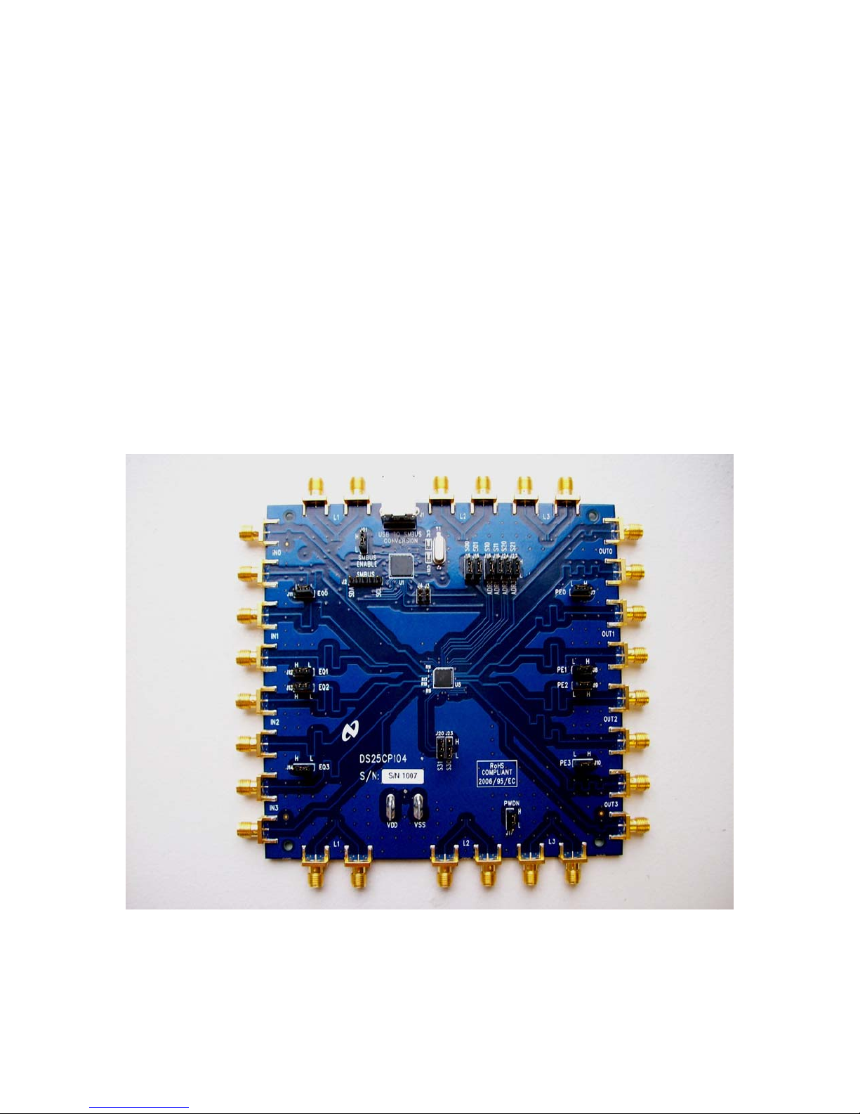
Figure 1. Photo of the DS25CP104EVK
Page 3 of 17
Page 4
DS25CP104EVK User Manual
DS25CP104EVK Description
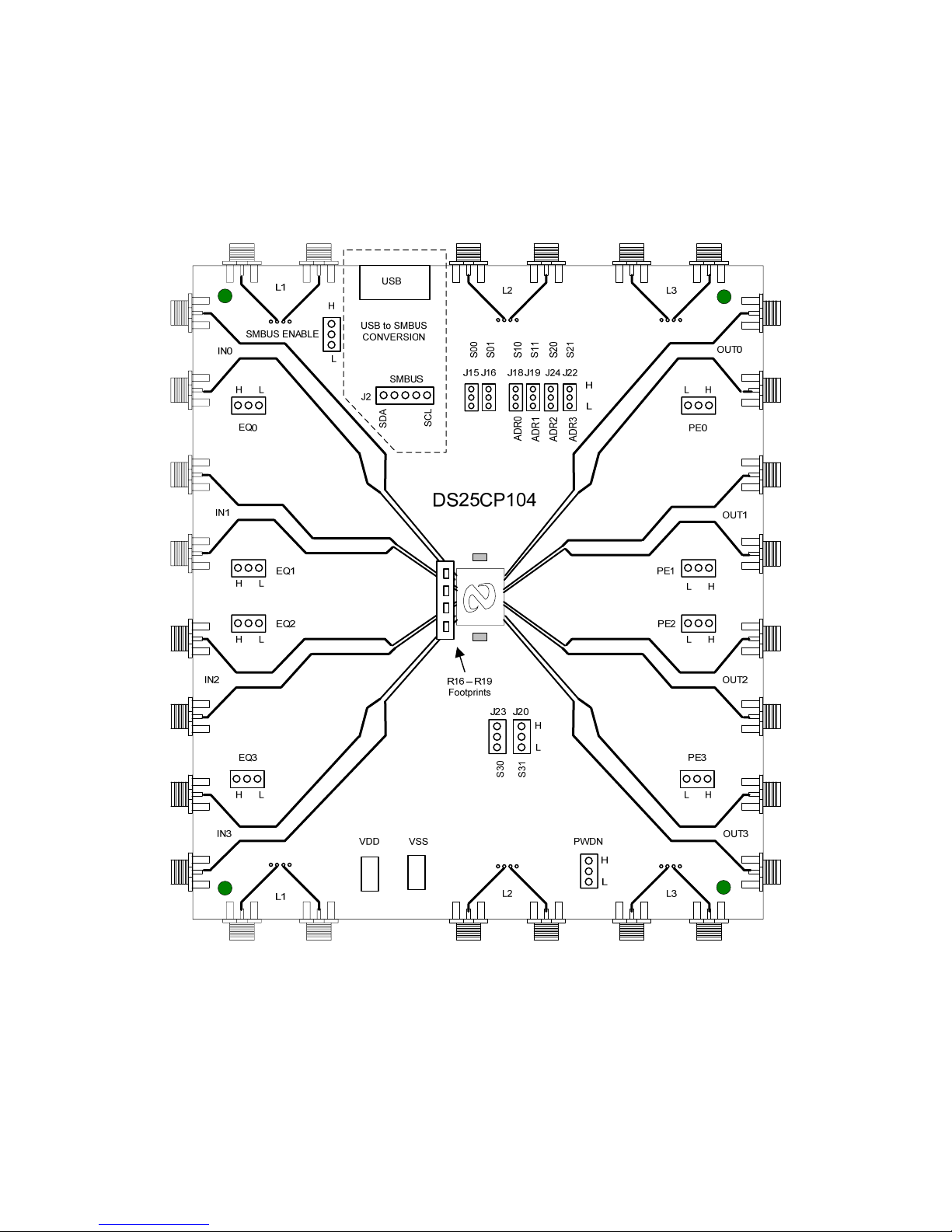
Figure 2 shows the top layer drawing of the PCB with the silkscreen annotations. The 4.5
by 4.5 inch, eight-layer PCB is designed to evaluate the functions of the DS25CP104.
Figure 2. Top Layer DS25CP104EVK
Page 4 of 17
Page 5
DS25CP104EVK User Manual
For descriptive purposes the DS25CP104EVK can be broken into three parts:
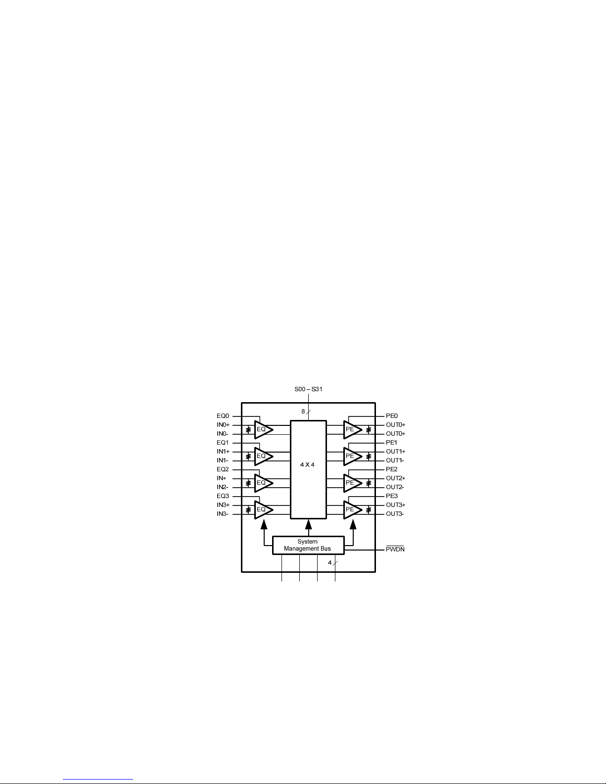
1. The DS25CP104 IC with associated connectors and jumpers is the main part of the
board. The block diagram of the DS25CP104 is shown in Figure 3. The receive buffers
can be set to Off and Low equalization by the external pins EQ0 – EQ3; the transmit
buffers can be set to Off and Med. levels of pre-emphasis by the external pins PE0 – PE3.
Since data capabilities are 3.125 Gbps, SMA connectors are used to ensure minimal loss.
More information can be found about the DS25CP104 on the data sheets.
2. A USB to SMBus converter has been added to the evaluation kit to implement
SMBus switch configuration to control the signal conditioning. Through the SMBus the
DS25CP104 currently features four levels (Off, Low, Medium, and High) of preemphasis and two levels (Off, Low) of equalization.
3. Three channels of stripline have been added to the evaluation kit to test the preemphasis and equalization functions (15” (38.1cm), 30” (76.2cm), and 60” (152.4cm) ).
In practical applications, devices often drive long backplanes or cables. To help reduce
jitter caused from long backplanes or cables, pre-emphasis can be used for the drivers and
equalization for the receivers.
SCL
SDA
EN_smb
ADDRn
Figure 3. DS25CP104 Block Diagram
Page 5 of 17
Page 6
DS25CP104EVK User Manual
DS25CP104 Evaluation
The DS25CP104 is a 3.125 Gbps LVDS Crosspoint Switch with four levels of transmit
pre-emphasis and two levels of receive equalization configured in the SMBus Mode and
two levels of transmit pre-emphasis and two levels of receive equalization configured via
external jumpers on the evaluation board in the Pin Mode.
Initial Pin Settings for Pin Mode Testing
Pin Setting Note
SMBus Enable L Disable SMbus
EQ0 – EQ 3 L Equalization off,
See table
PE0 – PE3 L Pre-Emphasis off,
See table
PWDN H Power Down off
Switch Configuration Truth Tables
S01 S00 Input Selected
0 0 IN0
0 1 IN1
1 0 IN2
1 1 IN3
Table 1. Input Select Pins Configuration for the Output OUT0
S11 S10 Input Selected
0 0 IN0
0 1 IN1
1 0 IN2
1 1 IN3
Table 2. Input Select Pins Configuration for the Output OUT1
Page 6 of 17
Page 7
DS25CP104EVK User Manual
S21 S20 Input Selected
0 0 IN0
0 1 IN1
1 0 IN2
1 1 IN3
Table 3. Input Select Pins Configuration for the Output OUT2
S31 S30 Input Selected
0 0 IN0
0 1 IN1
1 0 IN2
1 1 IN3
Table 4. Input Select Pins Configuration for the Output OUT3
Signal Conditioning Tables
Output OUTn, n={0,1,2,3}
Pre-Emphasis Control Pin (PEn) State Pre-Emphasis Level
0 Off
1 Medium
Table 5. Transmit Pre-emphasis Truth Table
Input INn, n={0,1,2,3}
Equalization Control Pin (EQn) State Equalization Level
0 Off
1 Low
Table 6. Receive Equalization Truth Table
Stripline Length Table (also known as Test Channels)
Stripline Length Loss (dB) @ 1250 MHz
L1 15” (38.1cm) -3.6
L2 30” (76.2cm) -8.2
L3 60” (152.4cm) -14.5
Table 7. Stripline length table
Page 7 of 17
Page 8
DS25CP104EVK User Manual
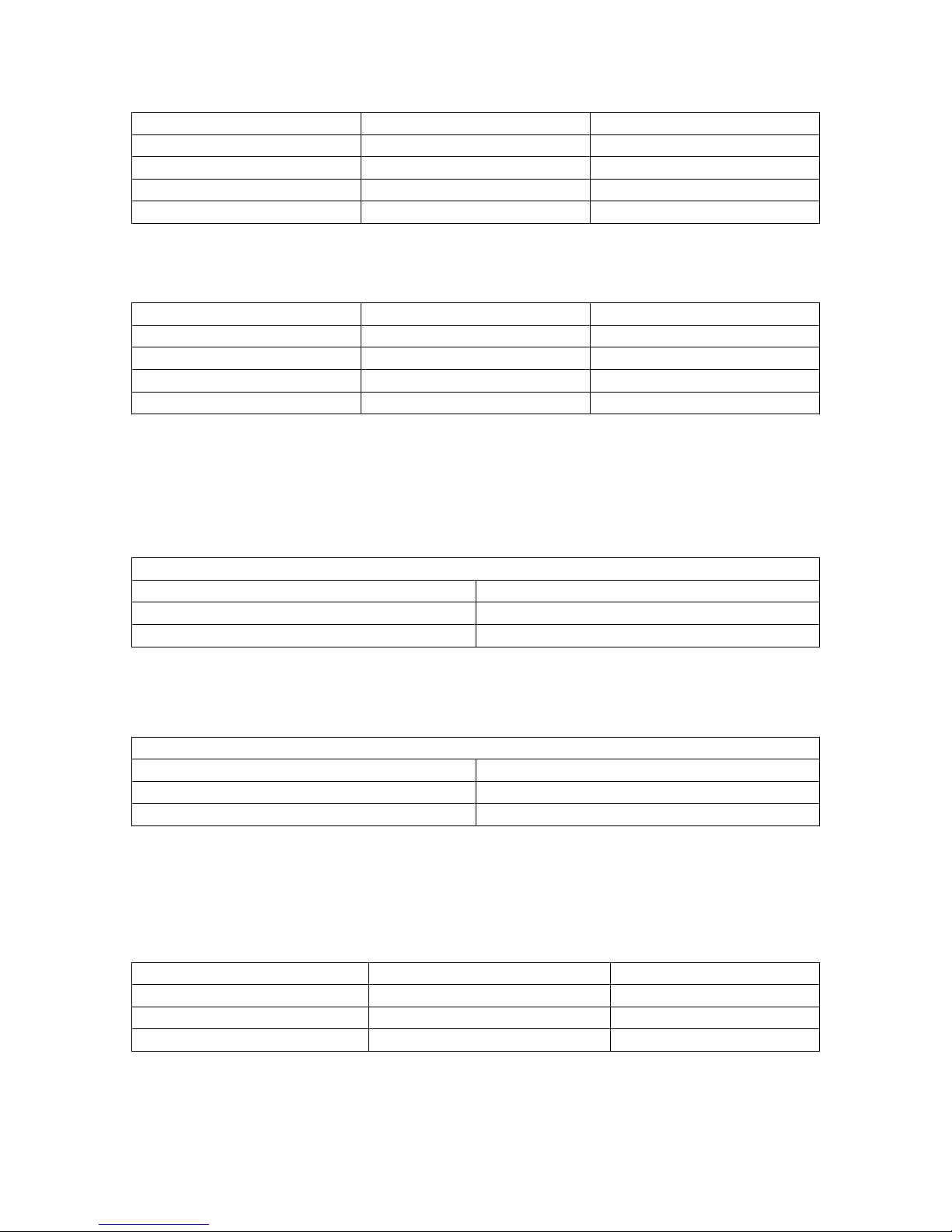
Jitter Performance Testing with No Signal Conditioning
1. Configure the test setup as shown in Figure 4.
2. Set the desired INn to OUTn drivers by selecting S00, S01, S10, S11, S20, S21,
S30, S31 according to Tables 1 – 4.
3. Select the PEn and EQn jumpers to 0, according to tables 5 and 6.
4. Apply + supply (3.3V typical) to the VDD and – supply (ground) to the VSS
connectors.
5. Connect a signal source (signal generator, data source, or an LVDS driver) to the
desired INn inputs on the board and adjust the signal parameters (VOH, VOL,
VCM) so that they comply with the device input recommendations.
6. Connect an oscilloscope to the selected OUTn outputs and view the output signals
with an oscilloscope with the bandwidth of at least 5 GHz.
Figure 4. Jitter Performance Test Circuit
Page 8 of 17
Page 9
DS25CP104EVK User Manual
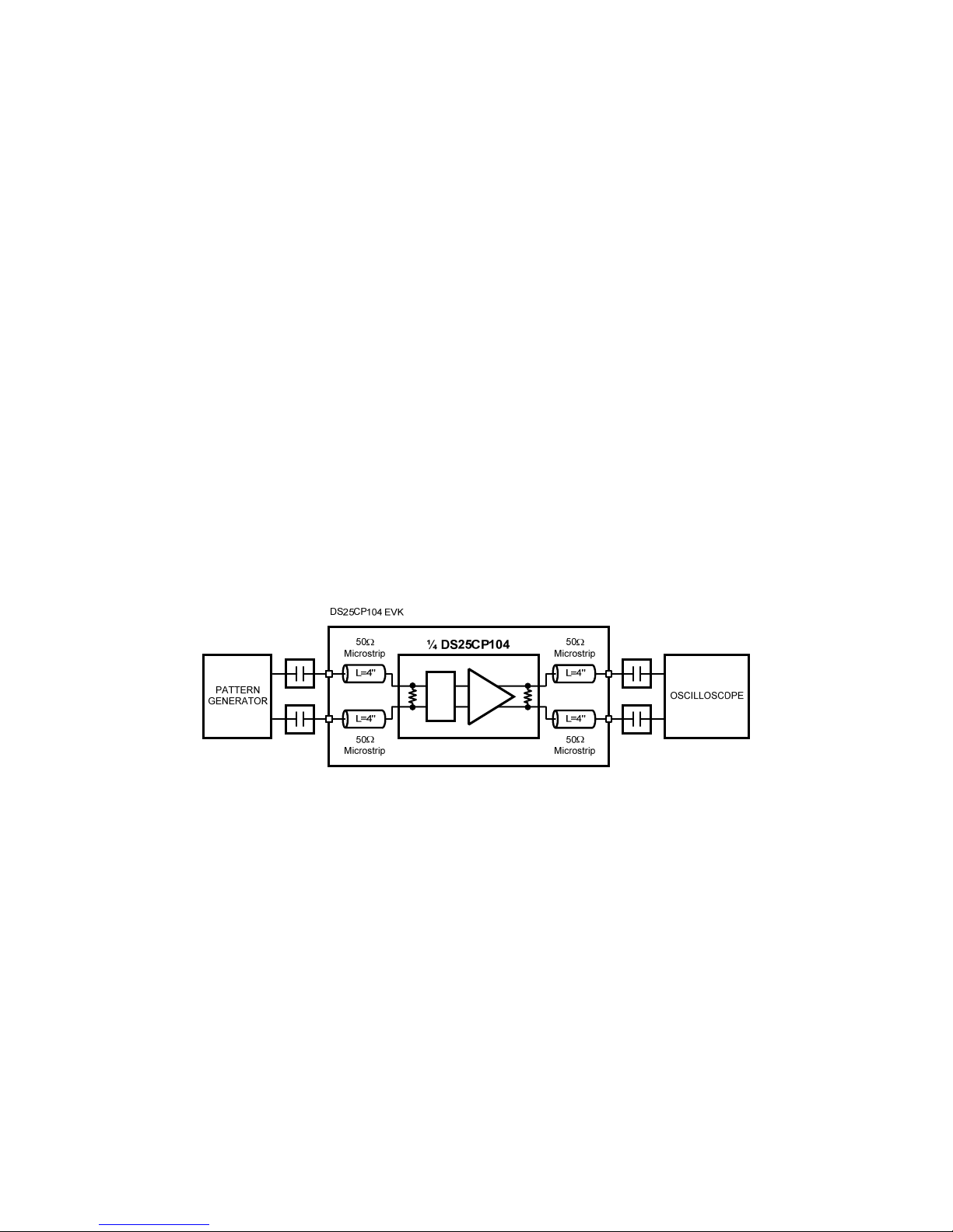
Pre-Emphasis Performance Testing
In applications where data transmits over cables or long backplanes, the pre-emphasis
feature on the DS25CP104 transmitter helps to overcome media loss and reduce bit
errors; hence the DS25CP104EVK has three lengths of stripline to test the pre-emphasis
function.
1. Configure the test setup as shown in figure 5; select the desired test channel
lengths in Table 7.
2. Set the desired INn to OUTn drivers by selecting S00, S01, S10, S11, S20, S21
according to Tables 1 – 4.
3. Select the PEn jumpers to 1 and the EQn jumpers to 0, according to Tables 5 and
6.
4. Apply + supply (3.3V typical) to the VDD and – supply (ground) to the VSS
connectors.
5. Connect a signal source (signal generator, data source, or an LVDS driver) to the
desired INn inputs on the board and adjust the signal parameters (VOH, VOL,
VCM) so that they comply with the device input recommendations.
6. Connect an oscilloscope to the selected OUTn outputs and view the output signals
with an oscilloscope with a bandwidth of at least 5 GHz.
Figure 5. Pre-Emphasis Performance Test Circuit
Page 9 of 17
Page 10
DS25CP104EVK User Manual
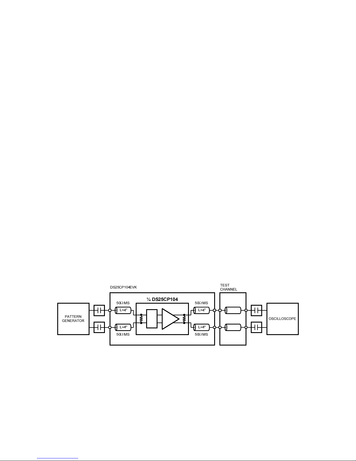
Equalization Performance Testing
In some applications, data transmits over cables or long backplanes. The equalization
function on the DS25CP104 receivers helps to compensate for loss of certain media;
hence the DS25CP104EVK has three lengths of stripline to test the equalization function.
1. Configure the test setup as shown in Figure 6; select the desired test channel,
lengths in Table 7.
2. Set the desired INn to OUTn drivers by selecting S00, S01, S10, S11, S20, S21,
S30, S31 according to Tables 1 – 4.
3. Select the PEn jumpers to 0 and the EQn jumpers to 1, according to Tables 5 and
6.
4. Apply + supply (3.3V typical) to the VDD and – supply (ground) to the VSS
connectors.
5. Connect a signal source (signal generator, data source, or an LVDS driver) to the
desired INn inputs on the board and adjust the signal parameters (VOH, VOL,
VCM) so that they comply with the device input recommendations.
6. Connect an oscilloscope to the selected OUTn outputs and view the output
signals with an oscilloscope with a bandwidth of at least 5 GHz.
Figure 6. Equalization Performance Test Circuit
Page 10 of 17
Page 11
DS25CP104EVK User Manual
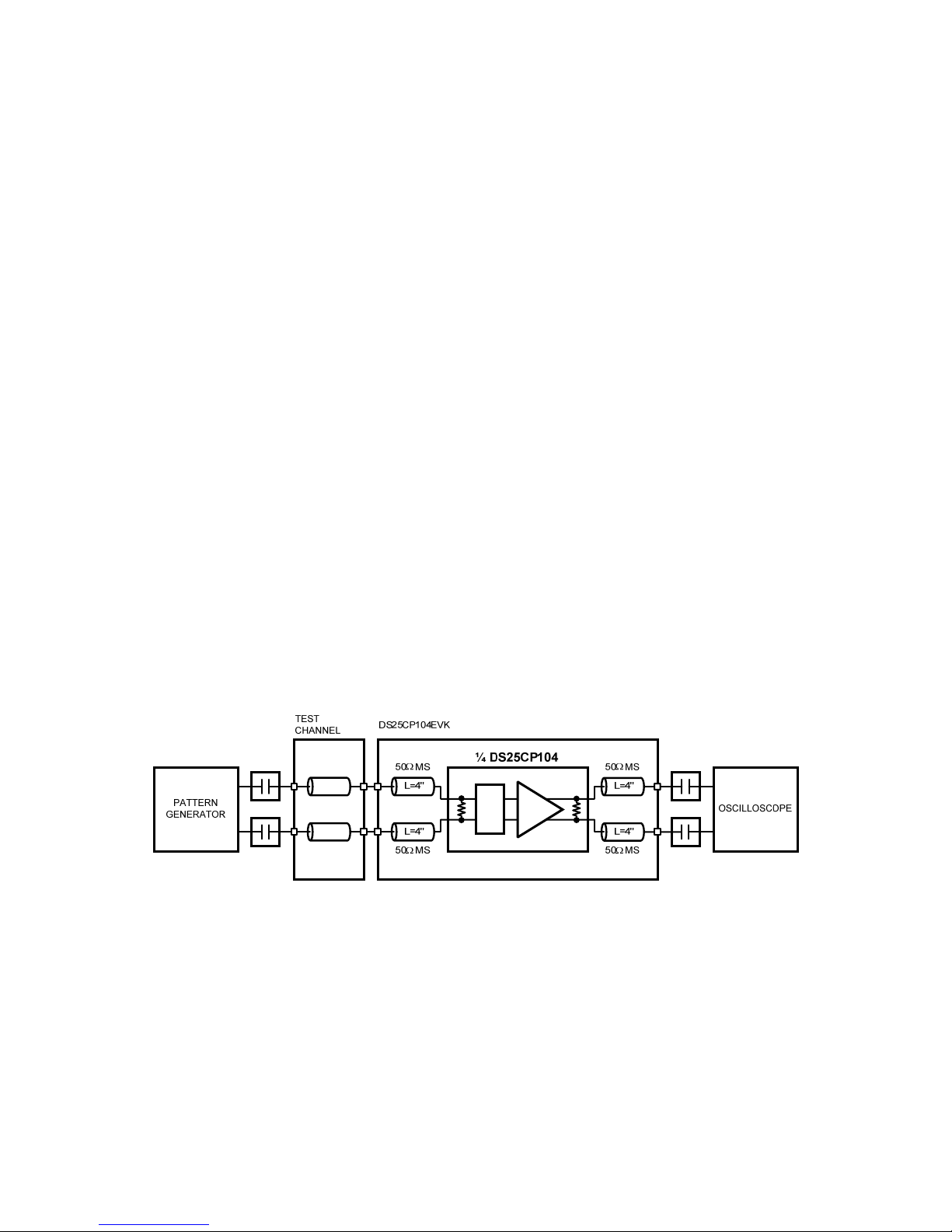
Pre-Emphasis and Equalization Performance Testing
In some applications, data transmits over cables or long backplanes. The pre-emphasis
and equalization functions on the DS25CP104 help to compensate for loss of certain
media; hence the DS25CP104EVK has three lengths of stripline to test the pre-emphasis
and equalization functions.
1. Configure the test setup as shown in Figure 7; select the desired test channel,
lengths in Table 7.
2. Set the desired INn to OUTn drivers by selecting S00, S01, S10, S11, S20, S21,
S30, S31 according to Tables 1 – 4.
3. Select the PEn jumpers to 1 and the EQn jumpers to 1, according to Tables 5 and
6.
4. Apply + supply (3.3V typical) to the VDD and – supply (ground) to the VSS
connectors.
5. Connect a signal source (signal generator, data source, or an LVDS driver) to the
desired INn inputs on the board and adjust the signal parameters (VOH, VOL,
VCM) so that they comply with the device input recommendations.
6. Connect an oscilloscope to the selected OUTn outputs and view the output
signals with an oscilloscope with a bandwidth of at least 5 GHz.
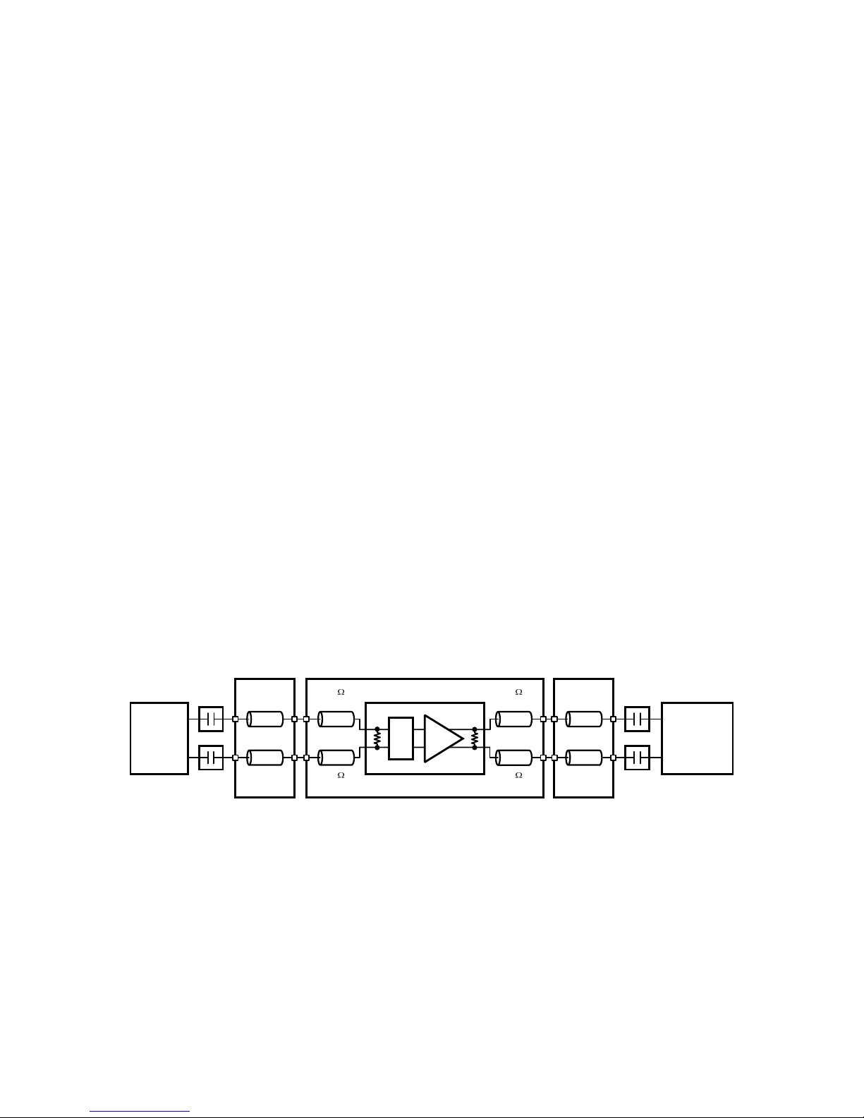
PATTERN
GENERATOR
TEST
CHANNEL
DS25CP104EVK
50
Microstrip
L=4"
L=4"
50
Microstrip
¼ DS25CP104
50
Microstrip
L=4"
L=4"
50
Microstrip
TEST
CHANNEL
OSCILLOSCOPE
Figure 7. Pre-emphasis and Equalization Performance Test Circuit
Page 11 of 17
Page 12

DS25CP104EVK User Manual
SMBus Evaluation
Introduction:
The CP104 can be evaluated in the Pin Mode using the external pins, or in the SMBus
mode. The following section describes how to load and run the Analog Launch Pad from
National Semiconductor, a proprietary interface, used to access the SMBus registers of
the CP104. The 1st time the application is run on a PC, and only the 1st time, the
application file needs to be downloaded, extracted, and then the appropriate driver needs
to be enabled. Any time after that, on the same PC, you need only to setup the
CP104EVK and then proceed to using the Analog Launch Pad.
Loading and running the application file
• Download the application file from
http://www.national.com/appinfo/lvds/ds25cp104evk.html
• Place in any folder on your PC, and run the file by double clicking on the file
from Windows Explorer (or My Computer); this will extract the file and place it
in C:\Program Files\National Semiconductor Corp folder.
• The Analog Launch Pad will now function only in the Demo mode.
• The Analog Launch Pad is designed to function on Windows 98/2000/xp
Setup the CP104EVK
(When using the USB, power should be off to the CP104 and USB unplugged when
changing cables or changing the jumper pins.)
1. Install jumper pins as follows:
J21, SMBus Enable
J4
J3
J15, J16
J18, J19
J24, J22
J20, J23
Table 8. Jumpers on the CP104EVK for SMBus use
2. Configure the test setup as desired, examples are fig. 4 – fig. 7.
3. Supply 3.3 V Power to board.
H Enables the SMBus
inserted USB Controller Reset
removed EEPROM write protect
removed S00 (SCL), S01 (SDA)
L Address
H Address
L
Page 12 of 17
Page 13

DS25CP104EVK User Manual
Load the driver
This needs to be done only once for a particular PC.
• Plug in the USB cable from the PC to the CP104 EVK; a small window should
appear in the lower right corner of the PC recognizing new hardware. If the
bubble says “USB device not recognized”, or nothing happens, check the
jumper configuration, if still does not work remove jumper on J4 for 5 sec,
and then replace. The USB controller is now reset and should be in
communication with the PC; this can be known by “Hi speed USB device plugged
into non Hi Speed USB hub” appearing in the window.
• Follow the instructions for New Hardware Wizard, which may take up to one
minute to run.
a. select “Install from a list or specific location”
b. select “Don’t search I will choose the driver to install”
c. select “Have disk”
d. Browse to “C:\Program Files\National Semiconductor Corp\Analog
LaunchPAD v1.07\Drivers”
e. select “NSC ALP Nano” from the list
f. install the driver
g. hit “Continue Anyway” if windows compatibility window is displayed
h. finish, you are now ready to run the Analog Launch Pad
Page 13 of 17
Page 14

DS25CP104EVK User Manual
Page 14 of 17
Page 15

DS25CP104EVK User Manual
Using the Analog Launch Pad for the CP104EVK
The Analog Launch Pad from National Semiconductor is a proprietary interface created
to assist developers to test their designs and systems using National’s evaluation boards;
the CP104EVK interface has been designed into the Analog Launch Pad. The registers of
the CP104 can be accessed through this interface enabling all the functions accessed
through the SMBus. Below is a picture of the Analog Launch Pad, CP104 interface:
Figure 8. Analog Launch Pad, CP104 interface
Page 15 of 17
Page 16

DS25CP104EVK User Manual
To use the interface:
• Run the application Analog Launch Pad and select CP104 Nano. For the Analog
Launch Pad to connect, the board must be powered with the appropriate jumper
selections and the USB driver must be functioning. Otherwise it will open into the
Demo mode.
• Select the “Register” folder and enter the register that you want to change, make
the appropriate changes, and then hit Apply. Register descriptions can be found in
the DS25CP104 datasheets.
• Use only Apply to make changes; Refresh, Refresh All, Display, Load, and
Save bubbles should not be used.
• A selected square corresponds to a ‘1’ while a blank square corresponds to a ‘0’.
• To change the levels of Pre Emphasis or Equalization, you must first go to
“Control” register and enable “Ignore External PE” and “Ignore External EQ”
before adjusting the signal conditioning through the SMBus.
• To use the “Loss of Signal”, you must first go to “Control” register and enable
“LOS”.
• The Verbose Description square switches to a more descriptive text.
Page 16 of 17
Page 17

DS25CP104EVK User Manual
• Typical Performance
When evaluating the CP104 EVK, the eye diagram response should be similar to those
below (measured on the Tektronix CSA 8000)
The DS25CP104 3.125 Gbps PRBS-7 output eye
diagram with no STRIPLINE connected and with
PE/EQ = Off
The DS25CP104 3.125 Gbps PRBS-7 output eye
diagram before the STRIPLINE2 (30” FR4) and
with PE/EQ = Off
The DS25CP104 3.125 Gbps PRBS-7 output eye
diagram after the STRIPLINE 1 (15” FR4) and with
EQ = Low. See Figure 6 for the Setup used.
The DS25CP104 3.125 Gbps PRBS-7 output eye
diagram before the STRIPLINE 2 (30” FR4) and
with PE = Med. See Figure 5 for the Setup used.
Page 17 of 17
Page 18

Page 19

Page 20

Item Part Type Part Number/Value Mfg Description Qty
SMTNoSub
Ref Des Notes
Rev
1 PCB P-05885R0 DS25CP104EVK: 5.25x5.25x.060in, 8 layer 1 0
Bd: (133.35x
133.35mm)
Panel: (
10.60x5.25in)
(269.24x
133.35mm) 2
bds/panel
2
3 IC 24LC128-I/SN MICROCHIP
128K bit Serial EEPROM 2.5V, SOIC8, PbFree
1 X 0U3
4 IC CY7C68013A-56LFXC CYPRESS
EZ-USB FX2 USB Microcontroller, QFN56,
Pb-Free
1 X 0U1
5 IC DS25CP104 NAT 1 0U5
Customer
Supplied
6 IC LP38691SD-3.3/NOPB NAT Linear Regulator, 3.3V, LLP6, Pb-Free 1 X 0U2
7 IC PGB1040805 LF ESD Suppressor, 0805, Pb-Free 1 X 0U4
8
9 RES ERJ-3GEY0R00 PANA 0 Ohm 1/10W ±5% 0603, Pb-Free 3 X 0R4,5,14
<ALT> CRCW06030000Z0EA VISHAY 0 Ohm 1/10W ±5% 0603, Pb-Free
<ALT> MCR03EZPJ000 ROHM 0 Ohm 1/10W ±5% 0603, Pb-Free
<ALT> RC0603JR-070RL YAGEO 0 Ohm 1/10W ±5% 0603, Pb-Free
10 RES ERJ-3GEYJ103 PANA 10K 1/10W ±5% 0603 200ppm, Pb-Free 5 X 0R3,8-9,12,13
<ALT> CRCW060310K0JNEA VISHAY 10K 1/10W ±5% 0603 200ppm, Pb-Free
<ALT> RK73B1JTTD103J KOA 10K 1/10W ±5% 0603 200ppm, Pb-Free
11 RES ERJ-3GEYJ220 PANA 22 Ohm 1/10W ±5% 0603 200ppm, Pb-Free 2 X 0R1-2
<ALT> CRCW060322R0JNEA VISHAY 22 Ohm 1/10W ±5% 0603 200ppm, Pb-Free
<ALT> RK73B1JTTD220J KOA 22 Ohm 1/10W ±5% 0603 200ppm, Pb-Free
12 RES ERJ-3GEYJ222 PANA 2.2K 1/10W ±5% 0603 200ppm, Pb-Free 2 X 0R6,7
<ALT> CRCW06032K20JNEA VISHAY 2.2K 1/10W ±5% 0603 200ppm, Pb-Free
<ALT> RK73B1JTTD222J KOA 2.2K 1/10W ±5% 0603 200ppm, Pb-Free
13 RES ERJ-8GEY0R00 PANA 0 Ohm 1/4W ±5% 1206, Pb-Free 2 X 0R10-11
1:12:35 PM, 4/20/2007
1 3
Page
of
Confidential and Proprietary. This document is considered uncontrolled unless stamped otherwise.
Creation Date:
3/28/2007
Responsible Eng/Mgr: Creator:
Arlene Fox
PL Number:
Z3071-01
Rev:
0
Rev Date:
3/28/2007
PL Status:
Released
Rev By:
Main Product:
PCBA, DS25CP104 EVK
TITLE:
NATIONAL SEMICONDUCTOR
PCBA, DS25CP104EVK, ROHS
ENERCON - BILL OF MATERIALS
Page 21

Item Part Type Part Number/Value Mfg Description Qty
SMTNoSub
Ref Des Notes
Rev
<ALT> CRCW12060000Z0EA VISHAY 0 Ohm 1/4W ±5% 1206, Pb-Free
14
15 CAP 0402YC103KAT AVX
.01µF, 16V, ±10%, 0402, Ceramic, X7R,
Pb-Free
2 X 0C15,17
<ALT> C0402C103K4RAC KEMET
.01µF, 16V, ±10%, 0402, Ceramic, X7R,
Pb-Free
<ALT> ECJ-0EB1C103K PANA
.01µF, 16V, ±10%, 0402, Ceramic, X7R,
Pb-Free
16 CAP 08055A180JAT AVX
18pF, 50V, ±5%, 0805, Ceramic, NP0, PbFree
2 X 0C11-12
<ALT> C0805C180J5GAC KEMET
18pF, 50V, ±5%, 0805, Ceramic, NP0, PbFree
<ALT> ECJ-2VC1H180J PANA
18pF, 50V, ±5%, 0805, Ceramic, NP0, PbFree
17 CAP C0402C104K8RAC KEMET
.1µF, 10V, ±10%, 0402, Ceramic, X7R, PbFree
10 X 0
C1,4-8,10,1314,16
18 CAP C1206C225K4RAC KEMET
2.2µF, 16V, ±10%, 1206, Ceramic, X7R,
Pb-Free
4 X 0C2,3,9,18
<ALT> ECJ-3YB1C225K PANA
2.2µF, 16V, ±10%, 1206, Ceramic, X7R,
Pb-Free
19
20 FILTER MMZ1608R301A TDK Ferrite, 300 Ohm, .5A, 0603, Pb Free 2 X 0FB1-2
21
22 XTAL HCM49-24.000MABJ CITIZEN Crystal, 24.0000MHz, SMD, 18pF, Pb-Free 1 X 0Y1
23
24 FUSE 1206L050 LF .5A, Resettable, SMT, .09 Ohms, Pb Free 1 X 0F1
25
26 CONN 1287-ST KEYSTONE Faston, Male, .250x.032, Pb-Free 2 0J25-26
27 CONN 142-0701-851 EMERSON SMA, Jack Receptacle, 50 OHM, Pb-Free 28 0SMA1-28
28 CONN 61729-0010 FCI USB-B, 4p, R/A, Pb-Free 1 0J1
29 CONN TSW-102-07-G-S SAMTEC Header, 2p, Male, .100"sp, Gold, Pb-Free 2 0J3-4
30 CONN TSW-103-07-G-S SAMTEC Header, 3p, Male, .100"sp, Gold, Pb-Free 18 0J7-24
1:12:35 PM, 4/20/2007
2 3
Page
of
Confidential and Proprietary. This document is considered uncontrolled unless stamped otherwise.
Creation Date:
3/28/2007
Responsible Eng/Mgr: Creator:
Arlene Fox
PL Number:
Z3071-01
Rev:
0
Rev Date:
3/28/2007
PL Status:
Released
Rev By:
Main Product:
PCBA, DS25CP104 EVK
TITLE:
NATIONAL SEMICONDUCTOR
PCBA, DS25CP104EVK, ROHS
ENERCON - BILL OF MATERIALS
Page 22

Item Part Type Part Number/Value Mfg Description Qty
SMTNoSub
Ref Des Notes
Rev
31 CONN TSW-105-07-G-S SAMTEC Header, 5p, Male, .100"sp, Gold, Pb-Free 1 0J2
32
33 STENCL T-05889R0 ENERCON STENCIL FABRICATION, TOP, DS25CP104EVK 1 0
34 STENCL T-05890R0 ENERCON
STENCIL FABRICATION, BOTTOM,
DS25CP104EVK
1 0
35
36 REF C-05886R0 ENERCON FABRICATION DWG, DS25CP104EVK 0
37 REF C-05888R0 ENERCON PALLET DWG, DS25CP104EVK 0
38 REF S-05887R0 ENERCON SCHEMATIC, DS25CP104EVK 0
39
40
41
Notes:
DO NOT STUFF:
R15,16,17,18,19
J5,6
1:12:35 PM, 4/20/2007
3 3
Page
of
Confidential and Proprietary. This document is considered uncontrolled unless stamped otherwise.
Creation Date:
3/28/2007
Responsible Eng/Mgr: Creator:
Arlene Fox
PL Number:
Z3071-01
Rev:
0
Rev Date:
3/28/2007
PL Status:
Released
Rev By:
Main Product:
PCBA, DS25CP104 EVK
TITLE:
NATIONAL SEMICONDUCTOR
PCBA, DS25CP104EVK, ROHS
ENERCON - BILL OF MATERIALS
Page 23

Page 24

Page 25

Page 26

Page 27

Page 28

Page 29

Page 30

Page 31

Page 32

Page 33

Page 34

Page 35

Page 36

 Loading...