

National Semiconductor DS25BR204 Technical data
DS25BR204
3.125 Gbps 1:4 LVDS Repeater with Transmit PreEmphasis and Receive Equalization
DS25BR204 3.125 Gbps 1:4 LVDS Repeater with Pre-Emphasis and Equalization
January 18, 2008
General Description
The DS25BR204 is a 3.125 Gbps 1:4 LVDS repeater optimized for high-speed signal routing and switching over lossy
FR-4 printed circuit board backplanes and balanced cables.
Fully differential signal paths ensure exceptional signal integrity and noise immunity.
The device has two different LVDS input channels and a select line determines which input is active. Both inputs have
programmable equalization providing maximum signal
strength. A loss-of-signal (LOS
channels and a unique LOS pin reports when no signal is detected at that input.
Wide input common mode range allows the switch to accept
signals with LVDS, CML and LVPECL levels; the output levels
are LVDS. A very small package footprint requires a minimal
space on the board while the flow-through pinout allows easy
board layout. Each differential input and output is internally
terminated with a 100Ω resistor to lower device return losses,
reduce component count and further minimize board space.
) circuit monitors both input
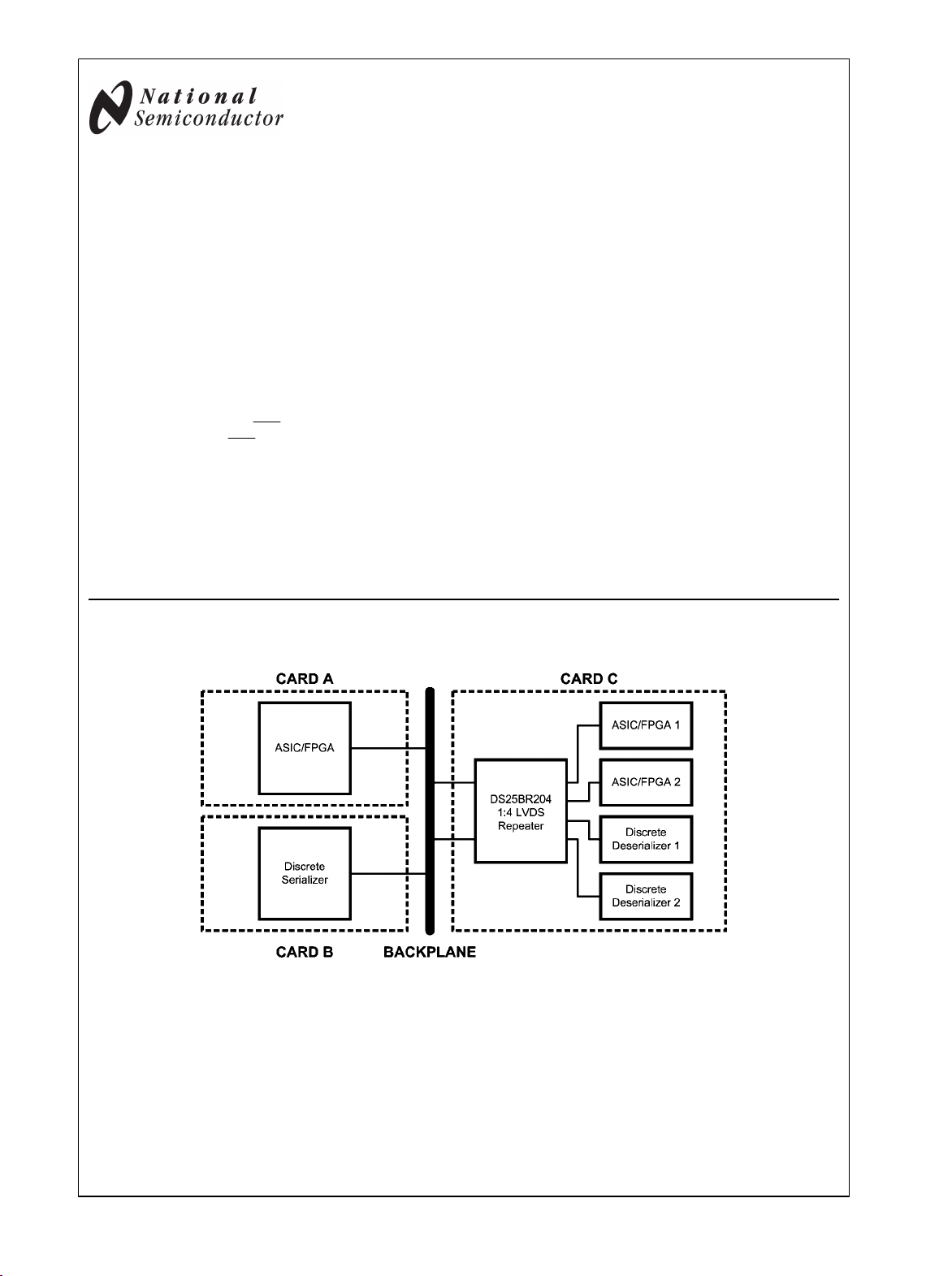
Typical Application
Features
DC - 3.125 Gbps low jitter, low skew, low power operation
■
Pin selectable transmit pre-emphasis and receive
■
equalization eliminate data dependant jitter
Wide Input Common Mode Range allows DC-coupled
■
interface to LVDS, CML and LVPECL drivers
Redundant inputs
■
Integrated 100Ω input and output terminations
■
8 kV ESD on LVDS I/O pins protects adjoining
■
components
Small 6 mm x 6 mm LLP-40 space saving package
■
Applications
Clock and data distribution
■
Clock and data buffering and muxing
■
OC-48 / STM-16
■
SD/HD/3GHD SDI Routers
■
30007703
© 2008 National Semiconductor Corporation 300077 www.national.com
Ordering Code
NSID Function Available Equalization
DS25BR204
DS25BR204TSQ 1:4 Repeater Off / On Off / On
Levels
Available Pre-Emphasis
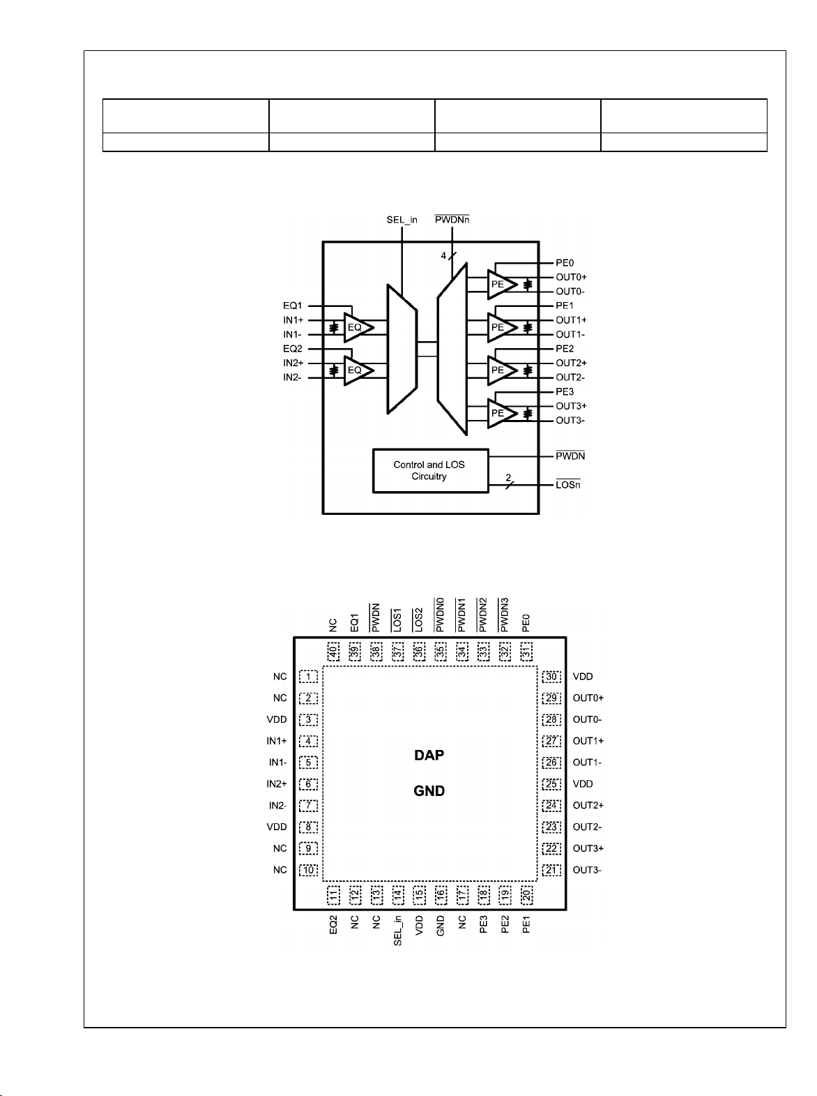
Block Diagram
Levels
Connection Diagram
30007701
DS25BR204 Pin Diagram
www.national.com 2
30007702
Pin Descriptions
DS25BR204
Pin Name Pin
Number
IN1+, IN1-,
IN2+, IN2-,
OUT0+, OUT0-,
OUT1+, OUT1-,
OUT2+, OUT2-,
OUT3+, OUT3-
EQ1, EQ2, 39,11 I, LVCMOS Receive equalization level select pins.
PE0, PE1,
PE2, PE3
SEL_in 14 I, LVCMOS Input select pin.
LOS2
LOS1
PWDN0,
PWDN1,
PWDN2,
PWDN3
NC 1, 2,
PWDN 38 I, LVCMOS Device power down pin. When the PWDN is set to L, the device
VDD 3, 8,
GND 16, DAP Power Ground pin and a pad (DAP - die attach pad).
4, 5,
6, 7,
29, 28,
27, 26,
24, 23,
22, 21
31, 20,
19, 18
36,
37
35,
34,
33,
32
9, 10,
12, 13,
17, 40
15,25, 30
I/O, Type Pin Description
I, LVDS Inverting and non-inverting high speed LVDS input pins.
O, LVDS Inverting and non-inverting high speed LVDS output pins.
I, LVCMOS Transmit pre-emphasis level select pins.
O, LVCMOS Loss of Signal output pin, LOSn, reports when an open input fault
condition is detected at the input, INn. These are open drain
outputs. External pull up resistors are required.
I, LVCMOS Channel output power down pins. When the PWDNn is set to L,
the channel output, OUTn, is in the power down mode.
NC NO CONNECT pins. May be left floating.
is in the power down mode.
Power Power supply pins.
3 www.national.com

Absolute Maximum Ratings (Note 4)
If Military/Aerospace specified devices are required,
please contact the National Semiconductor Sales Office/
Distributors for availability and specifications.
DS25BR204
Supply Voltage −0.3V to +4V
LVCMOS Input Voltage −0.3V to (VCC + 0.3V)
LVCMOS Output Voltage −0.3V to (VCC + 0.3V)
LVDS Input Voltage −0.3V to +4V
LVDS Differential Input Voltage 0.0V to +1V
LVDS Output Voltage −0.3V to (VCC + 0.3V)
LVDS Differential Output Voltage 0.0V to +1V
LVDS Output Short Circuit Current
Duration
Junction Temperature +150°C
Storage Temperature Range −65°C to +150°C
Lead Temperature Range
Soldering (4 sec.) +260°C
Maximum Package Power Dissipation at 25°C
SQA Package 4.65W
Derate SQA Package 37.2 mW/°C above +25°C
5 ms
Package Thermal Resistance
θ
θ
JA
JC
+26.9°C/W
+3.8°C/W
ESD Susceptibility
HBM (Note 1)
MM (Note 2)
CDM (Note 3)
Note 1: Human Body Model, applicable std. JESD22-A114C
Note 2: Machine Model, applicable std. JESD22-A115-A
Note 3: Field Induced Charge Device Model, applicable std.
JESD22-C101-C
Recommended Operating Conditions
Min Typ Max Units
Supply Voltage (VCC) 3.0 3.3 3.6 V
Receiver Differential Input
Voltage (VID)
Operating Free Air
Temperature (TA)
0 1 V
−40 +25 +85 °C
Electrical Characteristics
Over recommended operating supply and temperature ranges unless otherwise specified. (Notes 6, 7, 10)
Symbol Parameter Conditions Min Typ Max Units
LVCMOS DC SPECIFICATIONS
V
IH
V
IL
I
IH
I
IL
V
CL
V
OL
LVDS INPUT DC SPECIFICATIONS
V
ID
V
TH
V
TL
V
CMR
I
IN
C
IN
R
IN
High Level Input Voltage 2.0 V
DD
Low Level Input Voltage GND 0.8 V
High Level Input Current VIN = 3.6V
0 ±10
VCC = 3.6V
Low Level Input Current VIN = GND
0 ±10
VCC = 3.6V
Input Clamp Voltage ICL = −18 mA, VCC = 0V −0.9 −1.5 V
Low Level Output Voltage IOL= 4 mA 0.4 V
Input Differential Voltage 0 1 V
Differential Input High Threshold
Differential Input Low Threshold
VCM = +0.05V or VCC-0.05V
0 +100 mV
−100 0 mV
Common Mode Voltage Range VID = 100 mV 0.05 VCC -
0.05
Input Current
VIN = 3.6V or 0V
VCC = 3.6V or 0V
Input Capacitance Any LVDS Input Pin to GND
Input Termination Resistor Between IN+ and IN-
±1 ±10
1.7 pF
100
≥8 kV
≥250V
≥1250V
V
μA
μA
V
μA
Ω
www.national.com 4
Symbol Parameter Conditions Min Typ Max Units
LVDS OUTPUT DC SPECIFICATIONS
V
ΔV
V
ΔV
I
OS
C
R
OD
OS
OUT
OUT
Differential Output Voltage
Change in Magnitude of VOD for Complimentary
OD
Output States
Offset Voltage
Change in Magnitude of VOS for Complimentary
OS
Output States
RL = 100Ω
RL = 100Ω
250 350 450 mV
-35 35 mV
1.05 1.2 1.375 V
-35 35 mV
Output Short Circuit Current (Note 8) OUT to GND -35 -55 mA
OUT to V
CC
Output Capacitance Any LVDS Output Pin to GND
Output Termination Resistor Between OUT+ and OUT-
7 55 mA
1.2 pF
100
Ω
SUPPLY CURRENT
I
I
CC
CCZ
Supply Current PE = OFF, EQ = OFF, PWDN = H 150 185 mA
Power Down Supply Current PWDN = L 47 65 mA
Note 4: “Absolute Maximum Ratings” indicate limits beyond which damage to the device may occur, including inoperability and degradation of device reliability
and/or performance. Functional operation of the device and/or non-degradation at the Absolute Maximum Ratings or other conditions beyond those indicated in
the Recommended Operating Conditions is not implied. The Recommended Operating Conditions indicate conditions at which the device is functional and the
device should not be operated beyond such conditions.
Note 5: The Electrical Characteristics tables list guaranteed specifications under the listed Recommended Operating Conditions except as otherwise modified
or specified by the Electrical Characteristics Conditions and/or Notes. Typical specifications are estimations only and are not guaranteed.
Note 6: Current into device pins is defined as positive. Current out of device pins is defined as negative. All voltages are referenced to ground except VOD and
ΔVOD.
Note 7: Typical values represent most likely parametric norms for VCC = +3.3V and TA = +25°C, and at the Recommended Operation Conditions at the time of
product characterization and are not guaranteed.
Note 8: Output short circuit current (IOS) is specified as magnitude only, minus sign indicates direction only.
DS25BR204
5 www.national.com
 Loading...