


November 6, 2007
DS25BR110
3.125 Gbps LVDS Buffer with Receive Equalization
DS25BR110 3.125 Gbps LVDS Buffer with Receive Equalization
General Description
The DS25BR110 is a single channel 3.125 Gbps LVDS buffer
optimized for high-speed signal transmission over lossy FR-4
printed circuit board backplanes and balanced metallic cables. A fully differential signal path ensures exceptional signal
integrity and noise immunity.
The DS25BR110 features four levels of receive equalization
(EQ), making it ideal for use as a receiver device. Other LVDS
devices with similar IO characteristics include the following
products. The DS25BR120 features four levels of pre-emphasis for use as an optimized driver device, while the
DS25BR100 features both pre-emphasis and equalization for
use as an optimized repeater device. The DS25BR150 is a
buffer/repeater with the lowest power consumption and does
not feature transmit pre-emphasis nor receive equalization.
Wide input common mode range allows the receiver to accept
signals with LVDS, CML and LVPECL levels; the output levels
are LVDS. A very small package footprint requires minimal
space on the board while the flow-through pinout allows easy
board layout. The differential inputs and outputs are internally
terminated with a 100Ω resistor to lower device input and output return losses, reduce component count, and further minimize board space.
Typical Application
Features
DC - 3.125 Gbps low jitter, high noise immunity, low power
■
operation
Four levels of receive equalization reduce ISI jitter
■
On-chip 100Ω input and output termination minimizes
■
insertion and return losses, reduces component count and
minimizes board space
7 kV ESD on LVDS I/O pins protects adjoining
■
components
Small 3 mm x 3 mm 8-LLP space saving package
■
Applications
Clock and data buffering
■
Metallic cable equalization
■
FR-4 equalization
■
30005310
© 2007 National Semiconductor Corporation 300053 www.national.com
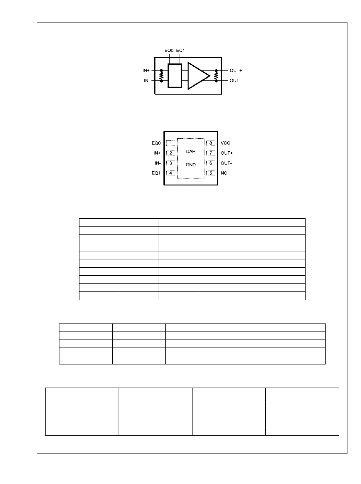
Block Diagram
DS25BR110
Pin Diagram
Pin Descriptions
30005303
30005306
Pin Name Pin Name Pin Type Pin Description
EQ0 1 Input Equalizer select pin.
IN+ 2 Input Non-inverting LVDS input pin.
IN- 3 Input Inverting LVDS input pin.
EQ1 4 Input Equalizer select pin.
NC 5 NA "NO CONNECT" pin.
OUT- 6 Output Inverting LVDS output pin.
OUT+ 7 Output Non-inverting LVDS Output pin.
VCC 8 Power Power supply pin.
GND DAP Power Ground pad (DAP - die attach pad)
Control Pins (EQ0 and EQ1) Truth Tables
EQ1 EQ0 Equalization Level
0 0 Off
0 1 Low (Approx. 4 dB at 1.56 GHz)
1 0 Medium (Approx. 8 dB at 1.56 GHz)
1 1 High (Approx. 16 dB at 1.56 GHz)
Ordering Codes and Configurations
NSID Function Available Equalization
Levels
DS25BR100TSD Buffer/Repeater Low / Medium Off / Medium
DS25BR110TSD Receiver Off / Low / Medium / High NA
DS25BR120TSD Driver NA Off / Low / Medium / High
DS25BR150TSD Buffer/Repeater NA NA
Available Pre-emphasis
Levels
www.national.com 2
DS25BR110
Absolute Maximum Ratings (Note 4)
If Military/Aerospace specified devices are required,
please contact the National Semiconductor Sales Office/
Distributors for availability and specifications.
Supply Voltage (VCC)
LVCMOS Input Voltage (EQ0, EQ1) −0.3V to (VCC + 0.3V)
LVDS Input Voltage (IN+, IN−) −0.3V to +4V
LVDS Differential Input Voltage ((IN+) - (IN−)) 0V to 1.0V
LVDS Output Voltage (OUT+, OUT−) −0.3V to (VCC + 0.3V)
LVDS Differential Output Voltage ((OUT+) - (OUT−)) 0V to 1.0V
LVDS Output Short Circuit Current
Duration
Junction Temperature +150°C
Storage Temperature Range −65°C to +150°C
Lead Temperature Range
Soldering (4 sec.) +260°C
Maximum Package Power Dissipation at 25°C
SDA Package 2.08W
Derate SDA Package 16.7 mW/°C above +25°C
−0.3V to +4V
5 ms
Package Thermal Resistance
θ
θ
JA
JC
+60.0°C/W
+12.3°C/W
ESD Susceptibility
HBM (Note 1)
MM (Note 2)
CDM (Note 3)
Note 1: Human Body Model, applicable std. JESD22-A114C
Note 2: Machine Model, applicable std. JESD22-A115-A
Note 3: Field Induced Charge Device Model, applicable std.
JESD22-C101-C
≥7 kV
≥250V
≥1250V
Recommended Operating Conditions
Min Typ Max Units
Supply Voltage (VCC) 3.0 3.3 3.6 V
Receiver Differential Input
Voltage (VID)
Operating Free Air
Temperature (TA)
1.0 V
−40 +25 +85 °C
DC Electrical Characteristics
Over recommended operating supply and temperature ranges unless otherwise specified. (Notes 5, 6, 7)
Symbol Parameter Conditions Min Typ Max Units
LVCMOS INPUT DC SPECIFICATIONS (EQ0, EQ1)
V
IH
V
IL
I
IH
I
IL
V
CL
LVDS OUTPUT DC SPECIFICATIONS (OUT+, OUT-)
V
OD
ΔV
V
OS
ΔV
I
OS
C
OUT
R
OUT
High Level Input Voltage 2.0 V
Low Level Input Voltage GND 0.8 V
High Level Input Current VIN = 3.6V
0 ±10
VCC = 3.6V
Low Level Input Current VIN = GND
0 ±10
VCC = 3.6V
Input Clamp Voltage ICL = −18 mA, VCC = 0V -0.9 −1.5 V
Differential Output Voltage
Change in Magnitude of VOD for Complimentary
OD
Output States
Offset Voltage
Change in Magnitude of VOS for Complimentary
OS
Output States
RL = 100Ω
RL = 100Ω
250 350 450 mV
-35 35 mV
1.05 1.2 1.375 V
-35 35 mV
Output Short Circuit Current (Note 8) OUT to GND -35 -55 mA
OUT to V
CC
Output Capacitance Any LVDS Output Pin to GND
7 55 mA
1.2 pF
Output Termination Resistor Between OUT+ and OUT- 100
CC
V
μA
μA
Ω
3 www.national.com
Symbol Parameter Conditions Min Typ Max Units
LVDS INPUT DC SPECIFICATIONS (IN+, IN-)
V
ID
V
DS25BR110
TH
V
TL
V
CMR
Input Differential Voltage 0 1 V
Differential Input High Threshold
Differential Input Low Threshold
VCM = +0.05V or VCC-0.05V
0 +100 mV
−100 0 mV
Common Mode Voltage Range VID = 100 mV 0.05 VCC -
0.05
I
IN
C
IN
R
IN
Input Current
Input Capacitance Any LVDS Input Pin to GND
Input Termination Resistor Between IN+ and IN-
VIN = 3.6V or 0V
VCC = 3.6V or 0V
±1 ±10
1.7 pF
100
SUPPLY CURRENT
I
CC
Supply Current EQ0 = 0, EQ1 = 0 35 43 mA
Note 4: “Absolute Maximum Ratings” indicate limits beyond which damage to the device may occur, including inoperability and degradation of device reliability
and/or performance. Functional operation of the device and/or non-degradation at the Absolute Maximum Ratings or other conditions beyond those indicated in
the Recommended Operating Conditions is not implied. The Recommended Operating Conditions indicate conditions at which the device is functional and the
device should not be operated beyond such conditions.
Note 5: The Electrical Characteristics tables list guaranteed specifications under the listed Recommended Operating Conditions except as otherwise modified
or specified by the Electrical Characteristics Conditions and/or Notes. Typical specifications are estimations only and are not guaranteed.
Note 6: Current into device pins is defined as positive. Current out of device pins is defined as negative. All voltages are referenced to ground except VOD and
ΔVOD.
Note 7: Typical values represent most likely parametric norms for VCC = +3.3V and TA = +25°C, and at the Recommended Operation Conditions at the time of
product characterization and are not guaranteed.
Note 8: Output short circuit current (IOS) is specified as magnitude only, minus sign indicates direction only.
V
μA
Ω
www.national.com 4
AC Electrical Characteristics (Note 11)
Over recommended operating supply and temperature ranges unless otherwise specified. (Notes 9, 10)
Symbol Parameter Conditions Min Typ Max Units
LVDS OUTPUT AC SPECIFICATIONS (OUT+, OUT-)
t
PHLD
t
PLHD
t
SKD1
t
SKD2
t
LHT
t
HLT
JITTER PERFORMANCE WITH EQ = OFF
t
RJ1A
t
RJ2A
t
DJ1A
t
DJ2A
t
TJ1A
t
TJ2A
Differential Propagation Delay High to Low
Differential Propagation Delay Low to High 350 465 ps
Pulse Skew |t
PLHD
− t
| (Note 12) 45 100 ps
PHLD
RL = 100Ω
350 465 ps
Part to Part Skew (Note 13) 45 150 ps
Rise Time
Fall Time 80 150 ps
Random Jitter (RMS Value)
No Test Channels
(Note 14)
Deterministic Jitter (Peak to Peak)
No Test Channels
(Note 15)
Total Jitter (Peak to Peak)
No Test Channels
(Note 16)
RL = 100Ω
VID = 350 mV
VCM = 1.2V
Clock (RZ)
EQ0 = 0, EQ1 = 0
VID = 350 mV
VCM = 1.2V
K28.5 (NRZ)
EQ0 = 0, EQ1 = 0
VID = 350 mV
VCM = 1.2V
PRBS-23 (NRZ)
EQ0 = 0, EQ1 = 0
2.5 Gbps 0.5 1 ps
3.125 Gbps 0.5 1 ps
2.5 Gbps 11 40 ps
3.125 Gbps 11 47 ps
2.5 Gbps 0.05 0.16
3.125 Gbps 0.08 0.20
80 150 ps
UI
UI
P-P
P-P
DS25BR110
5 www.national.com
 Loading...