

查询DS2003C供应商
DS2003/DS9667/DS2004
High Current/Voltage Darlington Drivers
General Description
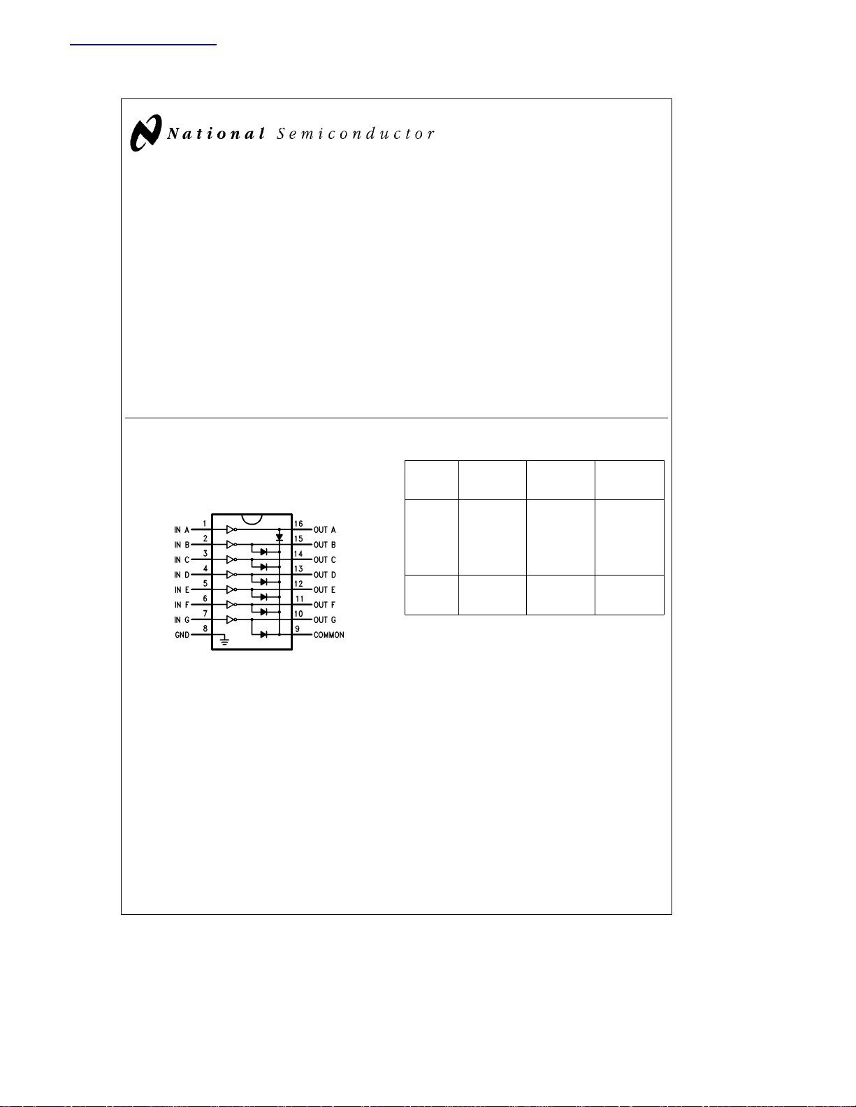
The DS2003/DS9667/DS2004 are comprised of seven high
voltage, high current NPN Darlington transistor pairs. All
units feature common emitter, open collector outputs. To
maximize their effectiveness, these units contain suppression diodes for inductive loads and appropriate emitter base
resistors for leakage.
The DS2003/DS9667 has a series base resistor to each
Darlington pair, thus allowing operation directly with TTL or
CMOS operating at supply voltages of 5.0V.
The DS2004 has an appropriate input resistor to allow direct
operation from CMOS or PMOS outputs operating from supply voltages of 6.0V to 15V.
December 1995
The DS2003/DS9667/DS2004 offer solutions to a great
many interface needs, including solenoids, relays, lamps,
small motors, and LEDs. Applications requiring sink currents
beyond the capability of a single output may be accommodated by paralleling the outputs.
Features
Y
Seven high gain Darlington pairs
Y
High output voltage (V
Y
High output current (I
Y
TTL, PMOS, CMOS compatible
Y
Suppression diodes for inductive loads
Y
Extended temperature range
C
CE
e
e
50V)
350 mA)
DS2003/DS9667/DS2004 High Current/Voltage Darlington Drivers
Connection Diagram
16-Lead DIP
Top View
Order Numbers
J Package N Package M Package
Number Number Number
J16A N16E M16A
DS2003 DS2003MJ DS2003TN DS2003TM
DS9667 DS2003TJ DS2003CN DS2003CM
DS2003CJ DS9667TN
DS9667MJ DS9667CN
DS9667TJ
DS9667CJ
DS2004 DS2004MJ DS2004TN DS2004TM
DS2004TJ DS2004CN DS2004CM
DS2004CJ
TL/F/9647– 1
C
1996 National Semiconductor Corporation RRD-B30M66/Printed in U. S. A.
TL/F/9647
Absolute Maximum Ratings (Note 1)
If Military/Aerospace specified devices are required,
please contact the National Semiconductor Sales
Office/Distributors for availability and specifications.
Storage Temperature Range
Ceramic DIP
Molded DIP
Operating Temperature Range
DS2003M/DS9667M
DS2004M
DS2003T/DS9667T
DS2004T
b
65§Ctoa175§C
b
65§Ctoa150§C
b
55§Ctoa125§C
b
55§Ctoa125§C
b
40§Ctoa105§C
b
40§Ctoa105§C
DS2003C/DS9667C 0§Ctoa85§C
DS2004C 0
Electrical Characteristics T
Ctoa85§C
§
e
25§C, unless otherwise specified (Note 2)
A
Symbol Parameter Conditions Min Typ Max Units
I
CEX
V
CE(Sat)
I
I(ON)
I
I(OFF)
V
I(ON)
C
I
t
PLH
t
PHL
I
R
V
F
Note 1: ‘‘Absolute Maximum Ratings’’ are those values beyond which the safety of the device cannot be guaranteed. They are not meant to imply that the devices
should be operated at these limits. The tables of ‘‘Electrical Characteristics’’ provide conditions for actual device operation.
Note 2: All limits apply to the complete Darlington series except as specified for a single device type.
Note 3: Under normal operating conditions these units will sustain 350 mA per output with V
30%.
Note 4: The I
Note 5: The V
Output Leakage T
Current
Collector-Emitter I
Saturation Voltage
Input Current V
Input Current T
(Note 4) I
Input Voltage V
(Note 5)
Input Capacitance 15 30 pF
Turn-On Delay 0.5 VIto 0.5 V
Turn-Off Delay 0.5 VIto 0.5 V
Clamp Diode V
Leakage Current T
Clamp Diode I
Forward Voltage
current limit guaranteed against partial turn-on of the output.
I(OFF)
voltage limit guarantees a minimum output sink current per the specified test conditions.
I(ON)
e
25§C, V
A
e
85§C, V
T
A
e
T
25§C, V
A
e
350 mA, I
C
e
200 mA, I
I
C
e
I
100 mA, I
C
e
3.85V
I
e
V
5.0V
I
e
V
12V
I
e
85§C for Commercial
A
e
500 mA
C
e
CE
e
V
CE
e
V
CE
e
V
CE
e
V
CE
e
V
CE
e
V
CE
e
50V
R
e
350 mA
F
(Figure 3)
(Figure 3)
(Figure 3)
2.0V, I
2.0V, I
2.0V, I
2.0V, I
2.0V, I
2.0V, I
2.0V, I
(Figure 6)
e
50V
CE
e
50V
CE
e
50V, V
CE
e
500 mA
B
e
350 mA
B
e
250 mA
B
(Figure 4)
e
200 mA
C
e
250 mA
C
e
300 mA
C
e
125 mA
C
e
200 mA
C
e
275 mA
C
e
350 mA
C
O
O
(Figure 7)
(Figure 1a)
(Figure 1a)
I
Lead Temperature
Ceramic DIP (Soldering, 60 seconds) 300
Molded DIP (Soldering, 10 seconds) 265
Maximum Power Dissipation* at 25§C
Cavity Package 2016 mW
Molded Package 1838 mW
S.O. Package 926 mW
*Derate cavity package 16.13 mW/§C above 25§C; derate molded DIP pack-
age 14.7 mW/
C above 25§C. Derate S.O. package 7.4 mW/§C.
§
Input Voltage 30V
Output Voltage 55V
Emitter-Base Voltage 6.0V
Continuous Collector Current 500 mA
Continuous Base Current 25 mA
for Commercial Grade 100 mA
e
1.0V
(Figure 2)
(Figure 1b)
(Note 3) 1.25 1.6
DS2004 500
(Figure 2)
(Figure 2)
DS2003/DS9667 0.93 1.35
DS2004 0.35 0.5
50 100 mA
(Figure 5)
DS2003/DS9667 2.4
(Figure 5)
(Figure 5)
(Figure 5)
DS2004 5.0
(Figure 5)
(Figure 5)
(Figure 5)
e
T
25§C50mA
A
e
85§C 100 mA
A
e
1.6V at 70§C with a pulse width of 20 ms and a duty cycle of
CE (Sat)
20
1.1 1.3 V
0.9 1.1
1.0 1.45
2.7
3.0
6.0
7.0
8.0
1.0 ms
1.0 ms
1.7 2.0 V
§
§
mA
C
C
V
http://www.national.com 2
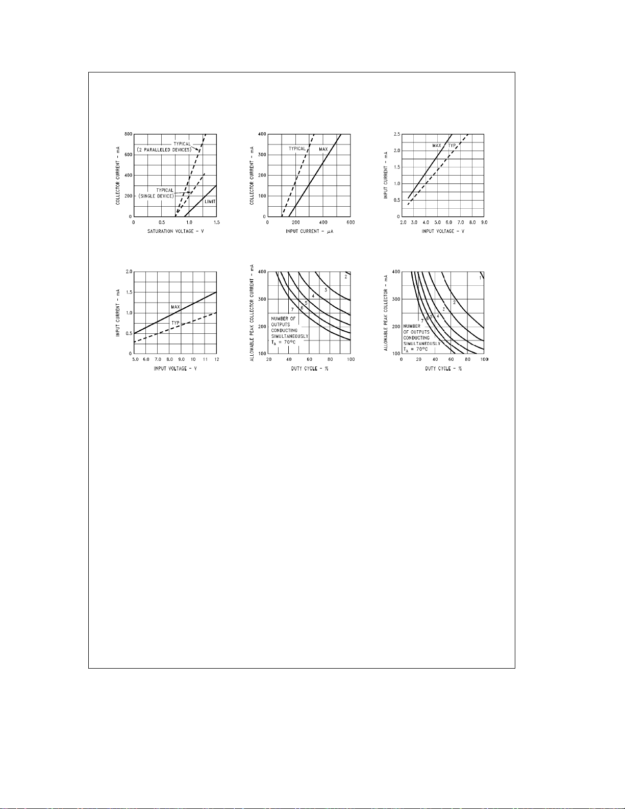
Typical Performance Characteristics
Collector Current vs
Saturation Voltage
DS2004
Input Current vs
Input Voltage
Collector Current vs
Input Current
Peak Collector Current vs
Duty Cycle and Number of
Outputs (Molded Package)
DS2003/DS9667
Input Current vs
Input Voltage
Peak Collector Current vs
Duty Cycle and Number of
Outputs (Ceramic Package)
TL/F/9647– 6
http://www.national.com3

Equivalent Circuits
Test Circuits
FIGURE 1a
FIGURE 3
TL/F/9647– 7
TL/F/9647– 10
TL/F/9647– 3
FIGURE 1b
FIGURE 4
TL/F/9647– 8
TL/F/9647– 11
TL/F/9647– 5
TL/F/9647– 9
FIGURE 2
TL/F/9647– 12
FIGURE 5
FIGURE 6
TL/F/9647– 13
http://www.national.com 4
FIGURE 7
TL/F/9647– 14

Typical Applications
Buffer for Higher Current Loads
TL/F/9647– 16
TL/F/9647– 17
http://www.national.com5

http://www.national.com 6

Physical Dimensions inches (millimeters) unless otherwise noted
Order Number DS2003CJ, DS9667CJ, DS2003MJ, D9667MJ,
DS2003TJ, DS9667TJ, DS2004CJ, DS2004MJ or DS2004TJ
Order Number DS2003CM, DS9667CM, DS2003TM, DS9667TM, DS2004CM or DS2004TM
Ceramic Dual-In-Line Package (J)
NS Package Number J16A
Surface Mount Package (M)
NS Package Number M16A
http://www.national.com7

Physical Dimensions inches (millimeters) unless otherwise noted (Continued)
Order Number DS2003CN, DS9667CN, DS2003TN, DS9667TN, DS2004CN or DS2004TN
Molded Dual-In-Line Package (N)
NS Package Number N16E
DS2003/DS9667/DS2004 High Current/Voltage Darlington Drivers
LIFE SUPPORT POLICY
NATIONAL’S PRODUCTS ARE NOT AUTHORIZED FOR USE AS CRITICAL COMPONENTS IN LIFE SUPPORT
DEVICES OR SYSTEMS WITHOUT THE EXPRESS WRITTEN APPROVAL OF THE PRESIDENT OF NATIONAL
SEMICONDUCTOR CORPORATION. As used herein:
1. Life support devices or systems are devices or 2. A critical component is any component of a life
systems which, (a) are intended for surgical implant support device or system whose failure to perform can
into the body, or (b) support or sustain life, and whose be reasonably expected to cause the failure of the life
failure to perform, when properly used in accordance support device or system, or to affect its safety or
with instructions for use provided in the labeling, can effectiveness.
be reasonably expected to result in a significant injury
to the user.
National Semiconductor National Semiconductor National Semiconductor National Semiconductor
Corporation Europe Hong Kong Ltd. Japan Ltd.
1111 West Bardin Road Fax:
Arlington, TX 76017 Email: europe.support@nsc.com Ocean Centre, 5 Canton Rd. Fax: 81-043-299-2408
Tel: 1(800) 272-9959 Deutsch Tel:
Fax: 1(800) 737-7018 English Tel:
http://www.national.com
National does not assume any responsibility for use of any circuitry described, no circuit patent licenses are implied and National reserves the right at any time without notice to change said circuitry and specifications.
Fran3ais Tel:
Italiano Tel:a49 (0) 180-534 16 80 Fax: (852) 2736-9960
a
49 (0) 180-530 85 86 13th Floor, Straight Block, Tel: 81-043-299-2308
a
49 (0) 180-530 85 85 Tsimshatsui, Kowloon
a
49 (0) 180-532 78 32 Hong Kong
a
49 (0) 180-532 93 58 Tel: (852) 2737-1600
 Loading...