

DS16EV5110
Video Equalizer (3D+C) for DVI, HDMI Sink-Side
Applications
DS16EV5110 Video Equalizer (3D+C) for DVI, HDMI Sink-Side Applications
July 17, 2008
General Description
The DS16EV5110 is a multi-channel equalizer optimized for
video cable extension sink-side applications. It operates between 250Mbps and 2.25Gbps with common applications at
1.65Gbps and 2.25Gbps (per data channel). It contains three
Transition-Minimized Differential Signaling (TMDS) data
channels and one clock channel as commonly found in DVI
and HDMI cables. It provides compensation for skin-effect
and dielectric losses, a common phenomenon when transmitting video on commercially available high definition video
cables.
The inputs conform to DVI and HDMI requirements and features programmable levels of input equalization. The programmable levels of equalization provide optimal signal boost
and reduces inter-symbol interference. Eight levels of boost
are selectable via a pin interface or by the optional System
Management Bus.
The clock channel is optimized for clock rates of up to 225
MHz and features a signal detect circuit. To maximize noise
immunity, the DS16EV5110 features a signal detector with
programmable thresholds. The threshold is adjustable
through a System Management Bus (SMBus) interface.
The DS16EV5110 also provides support for system power
management via output enable controls. Additional controls
are provided via the SMBus enabling customization and optimization for specific applications requirements. These controls include programmable features such as output amplitude and boost controls as well as system level diagnostics.
Features
8 levels of equalization settable by 3 pins or through the
■
SMBus interface
DC-Coupled inputs and outputs
■
Optimized for operation from 250 Mbps to 2.25 Gbps in
■
support of UXGA, 480 I/P, 720 I/P, 1080 I, and 1080 P with
8, 10, and 12–bit Color Depth Resolutions
Two DS16EV5110 devices support DVI/HDMI Dual Link
■
DVI 1.0, and HDMI 1.3a Compatible TMDS Interface
■
Clock channel signal detect (LOS)
■
Enable for power savings standby mode
■
System Management Bus (SMBus) provides control of
■
boost, output amplitude, enable, and clock channel signal
detect threshold
Low power consumption: 475mW (Typical)
■
0.13 UI total jitter at 1.65 Gbps including cable
■
Single 3.3V power supply
■
Small 7mm x 7mm, 48-pin leadless LLP package
■
-40°C to +85°C operating temperature range
■
Extends TMDS cable reach over:
■
1.
> 40 meters 24 AWG DVI Cable (1.65Gbps)
2.
> 20 meters 28 AWG DVI Cable (1.65Gbps)
3.
> 20 meters Cat5/Cat5e/Cat6 cables (1.65Gbps)
4.
> 20 meters 28 AWG HDMI cables (2.25Gbps)
Applications
Sink–side Video Applications:
■
Projectors
■
High Definition Displays
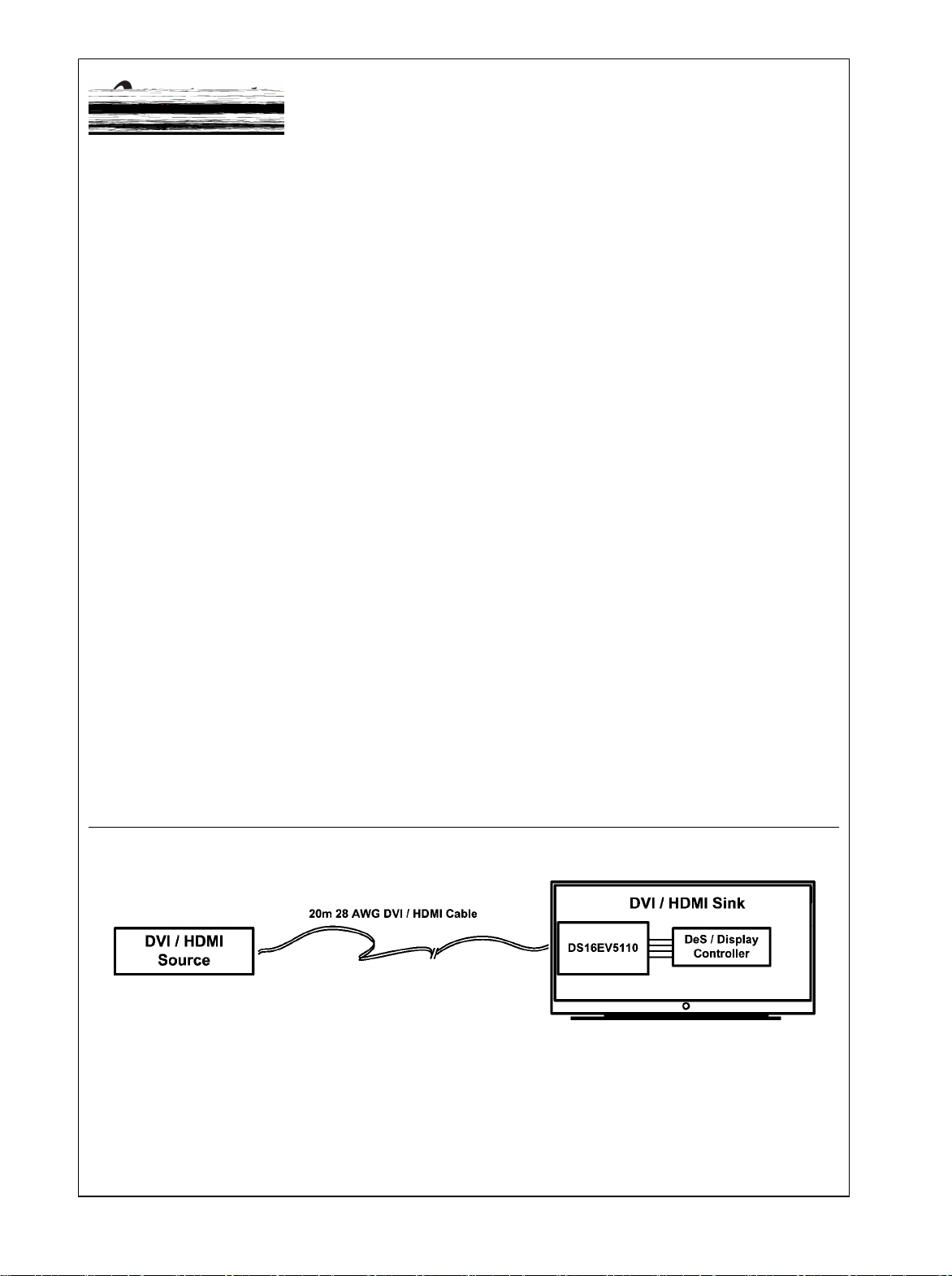
■
Typical Application
20216251
© 2008 National Semiconductor Corporation 202162 www.national.com
Pin Descriptions
Pin Name Pin Number I/O, Type Description
HIGH SPEED DIFFERENTIAL I/O
DS16EV5110
C_IN−
C_IN+
D_IN0−
D_IN0+
D_IN1−
D_IN1+
D_IN2−
D_IN2+
C_OUT-
C_OUT+
D_OUT0−
D_OUT0+
D_OUT1–
D_OUT1+
D_OUT2−
D_OUT2+
Equalization Control
BST_0
BST_1
BST_2
Device Control
EN 44 I, LVCMOS Enable Equalizer input. When held High, normal operation is selected. When held Low,
FEB 21 I, LVCMOS Force External Boost. When held High, the equalizer boost setting is controlled by the BST_
SD 45 O, LVCMOS Equalizer Clock Channel Signal Detect Output. Produces a High when signal is detected.
POWER
V
DD
GND 22, 24,
Exposed
Pad
System Management Bus (SMBus) Interface Control Pins
SDA 18 IO,
SDC 17 I, LVCMOS SMBus Clock Input. Internally pulled High to 3.3V with High-Z pull up.
CS 16 I, LVCMOS SMBus Chip select. When held High, the equalizer SMBus register is enabled. When held
Other
Reserv 19, 20, 38,
Note: I = Input, O = Output, IO =Input/Output,
1
2
4
5
8
9
11
12
36
35
33
32
29
28
26
25
23
14
37
3, 6, 7,
10, 13,
15, 46
27, 30,
31, 34
DAP GND The exposed pad at the center of the package must be connected to the ground plane.
39, 40,41,
42, 43, 47,
48
I, CML
I, CML
I, CML
I, CML
O, CML Inverting and non-inverting TMDS outputs from the equalizer. Open collector.
O, CML Inverting and non-inverting TMDS outputs from the equalizer. Open collector.
O, CML Inverting and non-inverting TMDS outputs from the equalizer. Open collector.
O, CML Inverting and non-inverting TMDS outputs from the equalizer. Open collector.
I, LVCMOS BST_0, BST_1, and BST_2 select the equalizer boost level for EQ channels. BST_0,
Power VDD pins should be tied to the VDD plane through a low inductance path. A 0.1µF bypass
GND Ground reference. GND should be tied to a solid ground plane through a low impedance
LVCMOS
Inverting and non-inverting TMDS Clock inputs to the equalizer. An on-chip 50Ω terminating
resistor connects C_IN+ to VDD and C_IN- to VDD.
Inverting and non-inverting TMDS Data inputs to the equalizer. An on-chip 50Ω terminating
resistor connects D_IN0+ to VDD and D_IN0- to VDD.
Inverting and non-inverting TMDS Data inputs to the equalizer. An on-chip 50Ω terminating
resistor connects D_IN1+ to VDD and D_IN1- to VDD.
Inverting and non-inverting TMDS Data inputs to the equalizer. An on-chip 50Ω terminating
resistor connects D_IN2+ to VDD and D_IN2- to VDD.
BST_1, and BST_2 are internally pulled Low. See Table 2.
standby mode is selected. EN is internally pulled High. Signal is global to all Data and Clock
channels.
[0:2] pins. When held Low, the equalizer boost level is controlled through the SMBus (see
Table 1) control pins. FEB is internally pulled High.
capacitor should be connected between each VDD pin to the GND planes.
path.
SMBus Data Input / Output. Internally pulled High to 3.3V with High-Z pull up.
Low, the equalizer SMBus register is disabled. CS is internally pulled Low. CS is internally
gated with SDC.
Reserved. Do not connect.
www.national.com 2
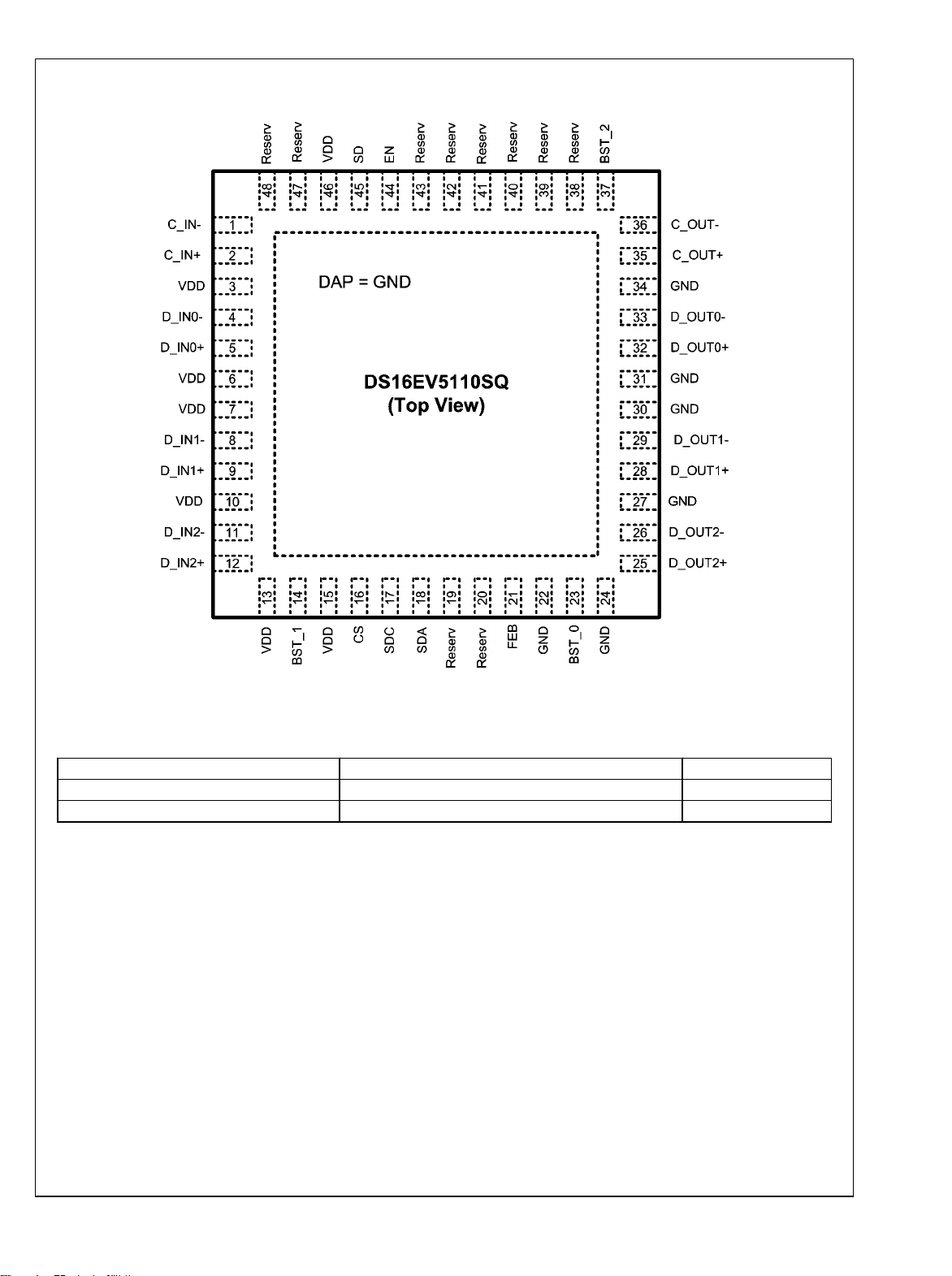
Connection Diagram
DS16EV5110
TOP VIEW — Not to Scale
Ordering Information
NSID Tape & Reel Quantity Package
DS16EV5110SQ 250 SQA48D
DS16EV5110SQX 2,500 SQA48D
20216252
3 www.national.com
Absolute Maximum Ratings (Note 1)
If Military/Aerospace specified devices are required,
please contact the National Semiconductor Sales Office/
Distributors for availability and specifications.
DS16EV5110
Supply Voltage (VDD)
LVCMOS Input Voltage -0.5V + 4.0V
LVCMOS Output Voltage -0.5V to 4.0V
CML Input/Output Voltage -0.5V to 4.0V
Junction Temperature +150°C
Storage Temperature -65°C to +150°C
Lead Temp. (Soldering, 5 sec.) +260°C
-0.5V to +4.0V
ESD Rating
HBM, 1.5 kΩ, 100 pF
CML Inputs >10 kV
Thermal Resistance
θJA, No Airflow
Recommended Operating Conditions (Notes 2, 3)
Min Typ Max Units
Supply Voltage
(VDD to GND)
Ambient Temperature -40 25 +85 °C
3.0 3.3 3.6 V
Electrical Characteristics
Over recommended operating supply and temperature ranges unless other specified. (Notes 2, 3)
Symbol Parameter Conditions Min Typ Max Units
LVCMOS DC SPECIFICATIONS
I
IH-PU
I
IH-PD
I
IL-PU
I
IL-PD
V
IH
V
IL
V
OH
V
OL
POWER
PD Power Dissipation EN = High, Device Enabled 475 700 mW
N Supply Noise Tolerance (Note 4) DC to 50MHz
CML INPUTS
V
TX
V
ICMDC
V
IN
R
LI
R
IN
CML OUTPUTS
V
O
V
OCM
tR, t
F
t
CCSK
High Level Input Leakage Current LVCMOS pins with internal pull-up
resistors
High Level Input Leakage Current LVCMOS pins with internal pull-
down resistors
Low Level Input Leakage Current LVCMOS pins with internal pull-up
resistors
Low Level Input Leakage Current LVCMOS pins with internal pull-
down resistors
High Level Input Voltage
Low Level Input Voltage
High Level Output Voltage SD Pin, IOH = -3mA
Low Level Output Voltage SD Pin, IOL = 3mA
-10 +10
80 105
-20 -10
-10 +10
2.0 VDD V
0 0.8 V
2.4 V
0.4 V
EN = Low, Power Down Mode 70 mW
Input Voltage Swing (Launch
Amplitude)
Input Common-Mode Voltage DC-Coupled Requirement
Input Voltage Swing Measured differentially at TPB
Differential Input Return Loss 100 MHz– 825 MHz, with fixture's
Input Resistance IN+ to VDD and IN− to VDD
Measured differentially at TPA
(Figure 2)
Measured at TPA (Figure 2)
(Figure 2)
effect de-embedded
800 1200
VDD-0.3
120
10 dB
45 50 55
Output Voltage Swing Measured differentially with OUT+
and OUT− terminated by 50Ω to
800 1200
VDD
Output common-mode Voltage Measured Single-ended VDD-0.3
Transition Time 20% to 80% of differential output
voltage, measured within 1" from
75 240 ps
output pins.
Inter Pair Channel-to-Channel
Skew (all 4 Channels)
Difference in 50% crossing
between shortest and longest
25 ps
channels
100
mV
VDD-0.2
VDD-0.2
>8 kV
30°C/W
μA
μA
μA
μA
mV
V
mV
Ω
mV
V
P-P
P-P
P-P
P-P
www.national.com 4

Symbol Parameter Conditions Min Typ Max
Electrical Characteristics — System Management Bus Interface (Notes 2, 3)
Over recommended operating supply and temperature ranges unless other specified.
Symbol Parameter Conditions Min Typ Max Units
DS16EV5110
System Bus Interface — DC Specifications
V
IL
V
IH
I
PULLUP
V
DD
I
LEAK-Bus
I
LEAK-Pin
C
I
R
TERM
System Bus Interface Timing Specification
FSMB Bus Operating Frequency (Note 12) 10 100 kHz
TBUF Bus Free Time Between Stop and
THD:STA Hold Time After (Repeated) Start
TSU:STA Repeated Start Condition Setup
TSU:STO Stop Condition Setup Time 4.0 µs
THD:DAT Data Hold Time 300 ns
TSU:DAT Data Setup Time 250 ns
T
TIMEOUT
T
LOW
T
HIGH
T
:SEXT Cumulative Clock Low Extend
LOW
t
F
t
R
t
POR
Data, Clock Input Low Voltage
Data, Clock Input High Voltage 2.8
Current through pull-up resistor or
VOL = 0.4V
current source
Nominal Bus Voltage 3.0
Input Leakage per bus segment (Note 9)
—200
Input Leakage per device pin
Capacitance for SDA and SDC (Notes 9, 10)
Termination Resistance V
Start Condition
Condition. First CLK generated
, (Notes 9, 10, 11)
DD3.3
At I
PULLUP
, Max
4.7
4.0 µs
after this period.
Time
Detect Clock Low Timeout (Note 12)
Clock Low Period
Clock High Period (Note 12)
4.7 µs
25 35 ms
4.7 µs
4.0 50 µs
(Note 12)
Time (Slave Device)
Clock/Data Fall Time (Note 12)
Clock/Data Rise Time (Note 12)
Time in which a device must be
(Note 12)
operational after power-on reset
10
0.8
V
DD
3.6
+200
—15
10 pF
1000
2 ms
300 ns
1000 ns
500 ms
V
V
mA
V
µA
µA
Ω
µs
Note 9: Recommended value. Parameter not tested in production.
Note 10: Recommended maximum capacitance load per bus segment is 400pF.
Note 11: Maximum termination voltage should be identical to the device supply voltage.
Note 12: Compliant to SMBus 2.0 physical layer specification. See System Management Bus (SMBus) Specification Version 2.0, section 3.1.1 SMBus common
AC specifications for details.
www.national.com 6

Timing Diagrams
DS16EV5110
20216250
FIGURE 1. SMBus Timing Diagram
FIGURE 2. Test Setup Diagram for Jitter Measurement
7 www.national.com
20216227

System Management Bus (SMBus) and Configuration Registers
The System Management Bus interface is compatible to SMBus 2.0 physical layer specification. The use of the Chip
DS16EV5110
Select signal is required. Holding the CS pin High enables
the SMBus port allowing access to the configuration registers.
Holding the CS pin Low disables the device's SMBus allowing
communication from the host to other slave devices on the
bus. In the STANDBY state, the System Management Bus
remains active. When communication to other devices on the
SMBus is active, the CS signal for the DS16EV5110s must
be driven Low.
The address byte for all DS16EV5110s is AC'h. Based on the
SMBus 2.0 specification, the DS16EV5110 has a 7-bit slave
address of 1010110'b. The LSB is set to 0'b (for a WRITE),
thus the 8-bit value is 1010 1100 'b or AC'h.
The SDC and SDA pins are 3.3V LVCMOS signaling and include high-Z internal pull up resistors. External low
impedance pull up resistors maybe required depending upon
SMBus loading and speed. Note, these pins are not 5V tolerant.
Transfer of Data via the SMBus
During normal operation the data on SDA must be stable during the time when SDC is High.
There are three unique states for the SMBus:
START: A High-to-Low transition on SDA while SDC is High
indicates a message START condition.
STOP: A Low-to-High transition on SDA while SDC is High
indicates a message STOP condition.
IDLE: If SDC and SDA are both High for a time exceeding
t
from the last detected STOP condition or if they are High
BUF
for a total exceeding the maximum specification for t
the bus will transfer to the IDLE state.
HIGH
then
SMBus Transactions
The device supports WRITE and READ transactions. See
Register Description table for register address, type (Read/
Write, Read Only), default value and function information.
Writing a Register
To write a register, the following protocol is used (see SMBus
2.0 specification).
1.
The Host (Master) selects the device by driving its
SMBus Chip Select (CS) signal High.
2.
The Host drives a START condition, the 7-bit SMBus
address, and a “0” indicating a WRITE.
3.
The Device (Slave) drives the ACK bit (“0”).
4.
The Host drives the 8-bit Register Address.
5.
The Device drives an ACK bit (“0”).
6.
The Host drive the 8-bit data byte.
7.
The Device drives an ACK bit (“0”).
8.
The Host drives a STOP condition.
9.
The Host de-selects the device by driving its SMBus CS
signal Low.
The WRITE transaction is completed, the bus goes IDLE and
communication with other SMBus devices may now occur.
Reading a Register
To read a register, the following protocol is used (see SMBus
2.0 specification).
1.
The Host (Master) selects the device by driving its
SMBus Chip Select (CS) signal High.
2.
The Host drives a START condition, the 7-bit SMBus
address, and a “0” indicating a WRITE.
3.
The Device (Slave) drives the ACK bit (“0”).
4.
The Host drives the 8-bit Register Address.
5.
The Device drives an ACK bit (“0”).
6.
The Host drives a START condition.
7.
The Host drives the 7-bit SMBus Address, and a “1”
indicating a READ.
8.
The Device drives an ACK bit “0”.
9.
The Device drives the 8-bit data value (register contents).
10.
The Host drives a NACK bit “1”indicating end of the
READ transfer.
11.
The Host drives a STOP condition.
12.
The Host de-selects the device by driving its SMBus CS
signal Low.
The READ transaction is completed, the bus goes IDLE and
communication with other SMBus devices may now occur.
Please see Table 1 for more information.
www.national.com 8

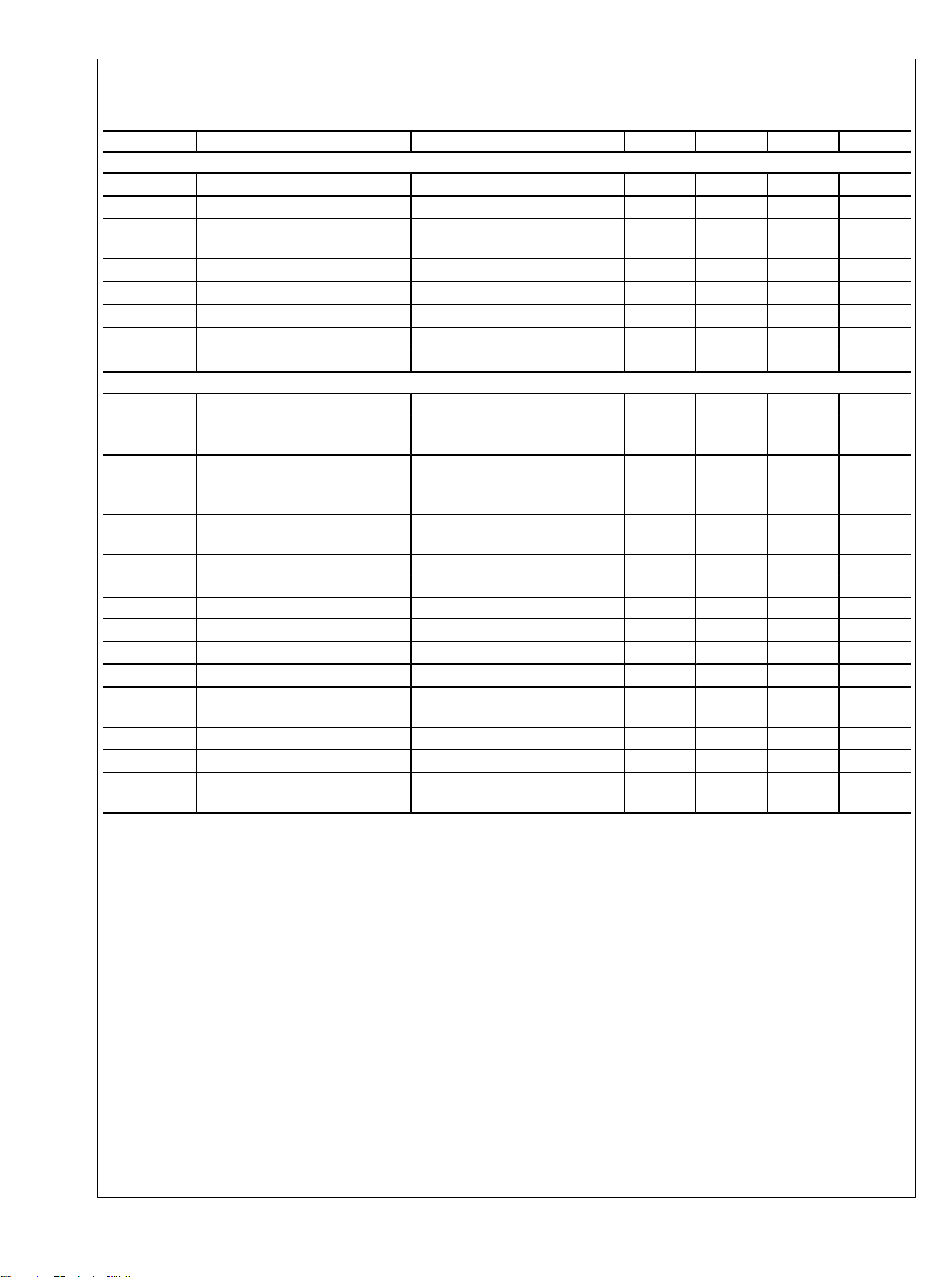
TABLE 1. SMBus Register Descriptions
Name Address Default Type Bit 7 Bit 6 Bit 5 Bit 4 Bit 3 Bit 2 Bit 1 Bit 0
Status 0x00 0x00 RO ID Revision Reserved Reserved Reserved SD
Status 0x01 0x00 RO Reserved Boost 1 EN Reserved
Status 0x02 0x00 RO Reserved Boost 3 Reserved Boost 2
Internal
Enable/
Individual
Channel
Boost
Control
for
C_IN±,
D_IN0±
0x03 0x77 RW EN (Int.)
0:Enable
1:Disable
(D_IN0±)
Boost Control
(BC for CH0)
000 (Min Boost)
001
010
011
100
101
110
EN (Int.)
0:Enable
1:Disable
(C_IN±)
Reserved
111 (Max Boost)
Individual
Channel
Boost
Control
for
D_IN1±,
D_IN2±
Signal
Detect ON
(SD_ON)
0x04 0x77 RW EN (Int.)
0:Enable
1:Disable
(D_IN2±)
Boost Control
(BC for CH2)
000 (Min Boost)
001
010
011
100
101
110
111 (Max Boost)
EN (Int.)
0:Enable
1:Disable
(D_IN1±)
Boost Control
(BC for CH1)
000 (Min Boost)
001
010
011
100
101
110
111 (Max Boost)
0x05 0x00 RW Reserved Threshold (mV)
00: 70 (Default)
01: 55
10: 90
11: 75
Signal
Detect OFF
(SD_OFF)
0x06 0x00 RW Reserved Threshold (mV)
00: 40 (Default)
01: 30
10: 55
11: 45
SMBus or
CMOS
Control for
EN
Output
Level
0x07 0x00 RW Reserved SMBus
Enable
0: Disable
1: Enable
0x08 0x78 RW Reserved Output Level:
Reserved
00: 540 mVp-p
01: 770 mVp-p
10: 1000 mVp-p
11: 1200 mVp-p
Note: RO = Read Only, RW = Read/Write
DS16EV5110
9 www.national.com

DS16EV5110 Device Description
The DS16EV5110 video equalizer comprises three data
channels, a clock channel, and a control interface including a
Systeml Management Bus (SMBus) port.
DS16EV5110
DATA CHANNELS
The DS16EV5110 provides three data channels. Each data
channel consists of an equalizer stage, a limiting amplifier, a
DC offset correction block, and a TMDS driver as shown in
Figure 3.
EQUALIZER BOOST CONTROL
The data channel equalizers support eight programmable levels of equalization boost. The state of the FEB pin determines
how the boost settings are controlled. If the FEB pin is held
High, then the equalizer boost setting is controlled by the
Boost Set pins (BST_[0:2]) in accordance with Table 2. If this
programming method is chosen, then the boost setting selected on the Boost Set pins is applied to all three data
channels. When the FEB pin is held Low, the equalizer boost
level is controlled through the SMBus. This programming
method is accessed via the appropriate SMBus registers (see
Table 1). Using this approach, equalizer boost settings can
be programmed for each channel individually. FEB is internally pulled High (default setting); therefore if left unconnected, the boost settings are controlled by the Boost Set pins
(BST_[0:2]). The range of boost settings provided enables the
DS16EV5110 to address a wide range of transmission line
path loss scenarios, enabling support for a variety of data
rates and formats.
TABLE 2. EQ Boost Control Table
Control Via
SMBus
BC_2, BC_1,
BC_0
(FEB = 0)
000 000 9
001 001 14
010 010 18
011 011 21
100 100 24
101 101 26
110 110 28
111 111 30
DEVICE STATE AND ENABLE CONTROL
The DS16EV5110 has an Enable feature which provides the
ability to control device power consumption. This feature can
Control Via Pins
BST_2, BST_1,
BST_0
(FEB = 1)
EQ Boost Setting
at 825 MHz (dB)
(TYP)
be controlled either via the Enable Pin (EN Pin) or via the
Enable Control Bit which is accessed through the SMBus port
(see Table 1 and Table 3). If Enable is activated, the data
channels and clock channel are placed in the ACTIVE state
and all device blocks function as described. The
DS16EV5110 can also be placed in STANDBY mode to save
power. In this mode only the control interface including the
SMBus port as well as the clock channel signal detection circuit remain active.
TABLE 3. Enable and Device State Control
Register 07[0]
(SMBus)
0 : Disable 1 X ACTIVE
0 : Disable 0 X STANDBY
1 : Enable X 0 ACTIVE
1 : Enable X 1 STANDBY
CLOCK CHANNEL
The clock channel incorporates a limiting amplifier, a DC offset correction, and a TMDS driver as shown in Figure 4.
CLOCK CHANNEL SIGNAL DETECT
The DS16EV5110 features a signal detect circuit on the clock
channel. The status of the clock signal can be determined by
either reading the Signal Detect bit (SD) in the SMBus registers (see Table 1) or by the state of the SD pin. A logic High
indicates the presence of a signal that has exceeded a specified threshold value (called SD_ON). A logic Low means that
the clock signal has fallen below a threshold value (called
SD_OFF). These values are programmed via the SMBus
(Table 1). If not programmed via the SMBus, the thresholds
take on the default values for the SD_OFF and SD_ON values
as indicated in Table 4. The Signal Detect threshold values
can be changed through the SMBus. All threshold values
specified are DC peak-to-peak differential signals (positive
signal minus negative signal) at the input of the device.
TABLE 4. Clock Channel Signal Detect Threshold Values
Bit 1 Bit 0 SD_OFF Threshold
0 0 40 (Default) 70 (Default)
0 1 30 55
1 0 55 90
1 1 45 75
EN Pin
(CMOS)
Register 06 (mV)
Register 03[3]
(EN Control)
(SMBus)
Device State
SD_ON Threshold
Register 05 (mV)
www.national.com 10

FIGURE 3. DS16EV5110 Data Channel
DS16EV5110
20216237
FIGURE 4. DS16EV5110 Clock Channel
OUTPUT LEVEL CONTROL
The output amplitude of the TMDS drivers for both the data
channels and the clock channel can be controlled via the SMBus (see Table 1). The default output level is 1000mV p-p.
The following Table presents the output level values supported:
TABLE 5. Output Level Control Settings – REG 0x08[3:2]
Bit 3 Bit 2 Output Level (mV)
0 0 540
0 1 770
1 0 1000 (default)
1 1 1200
AUTOMATIC ENABLE FEATURE
It may be desired for the DS16EV5110 to be configured to
automatically enter STANDBY mode if no clock signal is
20216238
present. STANDBY mode can be implemented by connecting
the Signal Detect (SD) pin to the external (LVCMOS) Enable
(EN) pin. In order for this option to function properly,
REG07[0] should be set to a “0” (default value). If the clock
signal applied to the clock channel input swings above the
SD_ON threshold specified in the threshold register via the
SMBus, then the SD pin is asserted High. If the SD pin is
connected to the EN pin, this will enable the equalizer, limiting
amplifier, and output buffer on the data channels and the limiting amplifier and output buffer on the clock channel; thus the
DS16EV5110 will automatically enter the ACTIVE state. If the
clock signal present falls below SD_OFF threshold specified
in the threshold register, then the SD pin will be asserted Low,
causing the aforementioned blocks to be placed in the
STANDBY state.
11 www.national.com

Application Information
The DS16EV5110 is used to recondition DVI/HDMI video signals or differential signals with similar characteristics after
signal loss and degradation due to transmission through a
DS16EV5110
length of shielded or unshielded cable. It is intended to be
used on the Sink-side of the video link. The DS16EV5110A
FIGURE 5. DS16EV5110 Sink-side application
maybe used on the Source or Sink side of the application. The
DS16EV5110 ESD protection circuitry will not support the
V
specification when the dowstream device (e.g. DES) is
OFF
powered ON and the DS16EV5110 is powered OFF. Figure
10 shows the CML output circuitry and the ESD protection
diode (current path). It is also not recommneded to enable the
DS16EV5110 CML outputs without a load attached.
20216239
The DS16EV5110 may also be used in certain Source-side
application with certain restrictions. The DS16EV5110 CML
outputs will not meet the VOFF parameter required by the
HDMI Compliance Test Specification (v1.3b) when the
DS16EV5110 is powered off and the sink device is powered
on. A current path will be enabled through the ESD protection
diode (see Figure 10). If full compliance is not required, the
DS16EV5110 may be used in repeater type application as
shown in Figure 6 .
20216224
FIGURE 6. DS16EV5110 Repeater Application with CAT 5 cable
DVI 1.0 AND HDMI V1.2a APPLICATIONS
A single DS16EV5110 can be used to implement cable extension solutions with various resolutions and screen refresh
rates. The range of digital serial rates supported is between
250 Mbps and 1.65 Gbps. For applications requiring ultrahigh resolution for DVI applications (e.g., QXGA and WQXGA), a “dual link” TMDS interface is required. This is easily
configured by using two DS16EV5110 devices as shown in
Figure 7.
www.national.com 12
Note the recommended connections between LVCMOS control pins. This provides the Automatic Enable feature for both
devices based on the one active clock channel. In many applications the SMBus is not required (device is pin controlled),
for this application simply leave the three SMBus pins open.
SDC and SDA are internally pulled High, and CS is internally
pulled Low, thus the SMBus is in the disabled state.

FIGURE 7. Connection in Dual Link Application
DS16EV5110
20216228
HDMI V1.3 APPLICATION
The DS16EV5110 can reliably extend operation to distances
greater than 20 meters of 28 AWG HDMI cable at 2.25 Gbps,
thereby supporting HDMI v1.3 for 1080p HDTV resolution
with 12-bit color depth. Please note that the Electrical Characteristics specified in this document have not been tested for
and are not guaranteed for 2.25 Gbps operation.
DC COUPLED DATA PATHS AND DVI/HDMI COMPLIANCE
The DS16EV5110 is designed to support TMDS differential
pairs with DC coupled transmission lines. It contains integrated termination resistors (50Ω), pulled up to VDD at the input
stage, and open collector outputs for DVI / HDMI for signal
swing.
13 www.national.com

CABLE SELECTION
At higher frequencies, longer cable lengths produce greater
losses due to the skin effect. The quality of the cable with
respect to conductor wire gauge and shielding heavily influences performance. Thicker conductors have lower signal
DS16EV5110
degradation per unit length. In nearly all applications, the
DS16EV5110 equalization can be set to 0x04, and equalize
up to 22 dB skin effect loss for all input cable configurations
at all data rates, without degrading signal integrity.
28 AWG STP DVI / HDMI CABLES RECOMMENDED BOOST SETTINGS
The following table presents the recommended boost control
settings for various data rates and cable lengths for 28 AWG
DVI/HDMI compliant configurations. Boost setting maybe
done via the three BST[2:0] pins or via the respective register
values.
TABLE 6. Boost Control Setting for STP Cables
Setting Data Rate 28 AWG DVI / HDMI
0x04 750 Mbps 0–25m
0x04 1.65 Gbps 0–20m
0x06 750 Mbps 25m to greater than 30m
0x06 1.65 Gbps 20m to greater than 25m
0x03 2.25 Gbps 0–15m
0x06 2.25 Gbps 15m to greater than 20m
Figure 8 shows the cable extension and jitter reduction obtained with the use of the equalizer. Table 6 lists the various
gain settings used versus cable length recommendations.
UTP (UNSHIELDED TWIST PAIRS) CABLES
The DS16EV5110 can be used to extend the length of UTP
cables, such as Cat5, Cat5e and Cat6 to distances greater
than 20 meters at 1.65 Gbps with < 0.13 UI of jitter. Please
note that for non-standard DVI/HDMI cables, the user must
ensure the clock-to-data channel skew requirements are met.
Table 7 presents the recommended boost control settings for
various data rates and cable lengths for UTP configurations:
TABLE 7. Boost Control Setting for UTP Cables
Setting Data Rate Cat5 Cable
0x03 750 Mbps 0–25m
0x06 750 Mbps 25–45m
0x03 1.65 Gbps Greater than 20m
Figure 9 shows the cable extension and jitter reduction obtained with the use of the equalizer. Table 7 lists the various
gain settings used versus cable length recommendations.
20216242
FIGURE 8. Equalized vs. Unequalized Jitter Performance
Over 28 AWG DVI/HDMI Cable
20216243
FIGURE 9. Equalized vs. Unequalized Jitter Performance
Over Cat5 Cable
www.national.com 14

DS16EV5110
General Recommendations
The DS16EV5110 is a high performance circuit capable of
delivering excellent performance. Careful attention must be
paid to the details associated with high-speed design as well
as providing a clean power supply. Refer to the LVDS
Owner’s Manual for more detailed information on high-speed
design tips as well as many other available resources available addressing signal integrity design issues.
PCB LAYOUT CONSIDERATIONS FOR DIFFERENTIAL PAIRS
The TMDS differential inputs and outputs must have a controlled differential impedance of 100Ω. It is preferable to route
TMDS lines exclusively on one layer of the board, particularly
for the input traces. The use of vias should be avoided if possible. If vias must be used, they should be used sparingly and
must be placed symmetrically for each side of a given differential pair. Route the TMDS signals away from other signals
and noise sources on the printed circuit board. All traces of
TMDS differential inputs and outputs must be equal in length
to minimize intra-pair skew.
LLP FOOTPRINT RECOMMENDATIONS
See National application note: AN-1187 for additional information on LLP packages footprint and soldering information.
POWER SUPPLY BYPASSING
Two approaches are recommended to ensure that the
DS16EV5110 is provided with an adequate power supply.
First, the supply (VDD) and ground (GND) pins should be
connected to power planes routed on adjacent layers of the
printed circuit board. The layer thickness of the dielectric
should be minimized so that the VDD and GND planes create
a low inductance supply with distributed capacitance. Second, careful attention to supply bypassing through the proper
use of bypass capacitors is required. A 0.1µF bypass capacitor should be connected to each VDD pin such that the
capacitor is placed as close as possible to the DS16EV5110.
Smaller body size capacitors can help facilitate proper component placement. Additionally, three capacitors with capacitance in the range of 2.2µF to 10µF should be incorporated
in the power supply bypassing design as well. These capacitors can be either tantalum or an ultra-low ESR ceramic and
should be placed as close as possible to the DS16EV5110.
EQUIVALENT I/O STRUCTURES
Figure 10 shows the DS16EV5110 CML output structure and
ESD protection circuitry.
Figure 11 shows the DS16EV5110 CML input structure and
ESD protection circuitry.
20216240
FIGURE 10. Equivalent Output Structure
FIGURE 11. Equivalent Input Structure
15 www.national.com
20216241

Typical Performance Characteristics
DS16EV5110
20216229 20216230
FIGURE 12. Un-equalized vs. Equalized Signal after 25m of 28 AWG DVI Cable at 1.65 Gbps (0x06 Setting)
20216231
FIGURE 13. Output Signal after 20m of Cat5 Cable at 1.65 Gbps (0x06 Setting)
20216232
FIGURE 14. Output Signal after 30m of 28 AWG DVI Cable at 750 Mbps (0x06 Setting)
www.national.com 16

20216233
FIGURE 15. Output Signal after 0.3m of 28 AWG DVI Cable at 1.65 Gbps (0x04 Setting)
DS16EV5110
20216234
FIGURE 16. Output Signal after 20m of 28 AWG HDMI Cable at 2.25 Gbps (0x06 Setting)
17 www.national.com

Physical Dimensions inches (millimeters) unless otherwise noted
DS16EV5110
7mm x 7mm 48-pin LLP Package
Order Number DS16EV5110SQ
To order lead-free products, call your National Semiconductor distributors. They can order products for you with an
"NOPB" specification. For more information on our Lead-free program, please check out our Lead-Free Status page.
Package Number SQA48D
www.national.com 18

Notes
DS16EV5110
19 www.national.com

Notes
For more National Semiconductor product information and proven design tools, visit the following Web sites at:
Products Design Support
Amplifiers www.national.com/amplifiers WEBENCH www.national.com/webench
Audio www.national.com/audio Analog University www.national.com/AU
Clock Conditioners www.national.com/timing App Notes www.national.com/appnotes
Data Converters www.national.com/adc Distributors www.national.com/contacts
Displays www.national.com/displays Green Compliance www.national.com/quality/green
Ethernet www.national.com/ethernet Packaging www.national.com/packaging
Interface www.national.com/interface Quality and Reliability www.national.com/quality
LVDS www.national.com/lvds Reference Designs www.national.com/refdesigns
Power Management www.national.com/power Feedback www.national.com/feedback
Switching Regulators www.national.com/switchers
LDOs www.national.com/ldo
LED Lighting www.national.com/led
PowerWise www.national.com/powerwise
Serial Digital Interface (SDI) www.national.com/sdi
Temperature Sensors www.national.com/tempsensors
Wireless (PLL/VCO) www.national.com/wireless
THE CONTENTS OF THIS DOCUMENT ARE PROVIDED IN CONNECTION WITH NATIONAL SEMICONDUCTOR CORPORATION
(“NATIONAL”) PRODUCTS. NATIONAL MAKES NO REPRESENTATIONS OR WARRANTIES WITH RESPECT TO THE ACCURACY
OR COMPLETENESS OF THE CONTENTS OF THIS PUBLICATION AND RESERVES THE RIGHT TO MAKE CHANGES TO
SPECIFICATIONS AND PRODUCT DESCRIPTIONS AT ANY TIME WITHOUT NOTICE. NO LICENSE, WHETHER EXPRESS,
IMPLIED, ARISING BY ESTOPPEL OR OTHERWISE, TO ANY INTELLECTUAL PROPERTY RIGHTS IS GRANTED BY THIS
DOCUMENT.
TESTING AND OTHER QUALITY CONTROLS ARE USED TO THE EXTENT NATIONAL DEEMS NECESSARY TO SUPPORT
NATIONAL’S PRODUCT WARRANTY. EXCEPT WHERE MANDATED BY GOVERNMENT REQUIREMENTS, TESTING OF ALL
PARAMETERS OF EACH PRODUCT IS NOT NECESSARILY PERFORMED. NATIONAL ASSUMES NO LIABILITY FOR
APPLICATIONS ASSISTANCE OR BUYER PRODUCT DESIGN. BUYERS ARE RESPONSIBLE FOR THEIR PRODUCTS AND
APPLICATIONS USING NATIONAL COMPONENTS. PRIOR TO USING OR DISTRIBUTING ANY PRODUCTS THAT INCLUDE
NATIONAL COMPONENTS, BUYERS SHOULD PROVIDE ADEQUATE DESIGN, TESTING AND OPERATING SAFEGUARDS.
EXCEPT AS PROVIDED IN NATIONAL’S TERMS AND CONDITIONS OF SALE FOR SUCH PRODUCTS, NATIONAL ASSUMES NO
LIABILITY WHATSOEVER, AND NATIONAL DISCLAIMS ANY EXPRESS OR IMPLIED WARRANTY RELATING TO THE SALE
AND/OR USE OF NATIONAL PRODUCTS INCLUDING LIABILITY OR WARRANTIES RELATING TO FITNESS FOR A PARTICULAR
PURPOSE, MERCHANTABILITY, OR INFRINGEMENT OF ANY PATENT, COPYRIGHT OR OTHER INTELLECTUAL PROPERTY
RIGHT.
LIFE SUPPORT POLICY
NATIONAL’S PRODUCTS ARE NOT AUTHORIZED FOR USE AS CRITICAL COMPONENTS IN LIFE SUPPORT DEVICES OR
SYSTEMS WITHOUT THE EXPRESS PRIOR WRITTEN APPROVAL OF THE CHIEF EXECUTIVE OFFICER AND GENERAL
DS16EV5110 Video Equalizer (3D+C) for DVI, HDMI Sink-Side Applications
COUNSEL OF NATIONAL SEMICONDUCTOR CORPORATION. As used herein:
Life support devices or systems are devices which (a) are intended for surgical implant into the body, or (b) support or sustain life and
whose failure to perform when properly used in accordance with instructions for use provided in the labeling can be reasonably expected
to result in a significant injury to the user. A critical component is any component in a life support device or system whose failure to perform
can be reasonably expected to cause the failure of the life support device or system or to affect its safety or effectiveness.
National Semiconductor and the National Semiconductor logo are registered trademarks of National Semiconductor Corporation. All other
brand or product names may be trademarks or registered trademarks of their respective holders.
Copyright© 2008 National Semiconductor Corporation
For the most current product information visit us at www.national.com
www.national.com
National Semiconductor
Americas Technical
Support Center
Email: support@nsc.com
Tel: 1-800-272-9959
National Semiconductor Europe
Technical Support Center
Email: europe.support@nsc.com
German Tel: +49 (0) 180 5010 771
English Tel: +44 (0) 870 850 4288
National Semiconductor Asia
Pacific Technical Support Center
Email: ap.support@nsc.com
National Semiconductor Japan
Technical Support Center
Email: jpn.feedback@nsc.com
 Loading...