

National Semiconductor DS15EA101 Technical data
DS15EA101
0.15 to 1.5 Gbps Adaptive Cable Equalizer with LOS
Detection
DS15EA101 0.15 to 1.5 Gbps Adaptive Cable Equalizer with LOS Detection
July 2007
General Description
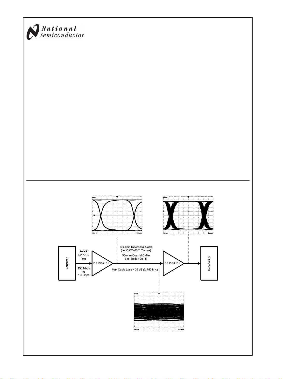
The DS15EA101 is an adaptive equalizer optimized for equalizing data transmitted over copper cables. The DS15EA101
operates over a wide range of data rates from 150 Mbps to
1.5+ Gbps and automatically adapts to equalize any cable
length from zero meters to lengths that attenuate the signal
by 35 dB at 750 MHz.
The DS15EA101 allows either single-ended or differential input drive. This enables equalization of coaxial cables as well
as differential twin-ax and twisted pair cables.
Additional features include an LOS output and an output enable which, when tied together, disable the output when no
signal is present.
The DS15EA101 is powered from a single 3.3V supply and
consumes 210 mW at 1.5 Gbps. It operates over the full
−40°C to +85°C industrial temperature range and is available
in a space saving 4 x 4 mm LLP-16 package which allows for
high density placement of components in multi-channel applications.
Typical Application
Features
Automatic equalization of coaxial, twin-ax and twisted pair
■
cables
High data rates: 150 Mbps to 1.5+ Gbps
■
Up to 35 dB of boost at 750 MHz
■
LOS detection and output enable
■
Single-ended or differential input
■
50Ω differential outputs
■
Low power operation, 210 mW (typ) at 1.5 Gbps
■
Industrial -40°C to +85°C temperature
■
Space-saving 4 x 4 mm LLP-16 package
■
Applications
Cable extention applications
■
Security cameras
■
Remote LCDs and LED panels
■
Data recovery equalization
■
20201701
© 2007 National Semiconductor Corporation 202017 www.national.com
Absolute Maximum Ratings (Note 1)
Supply Voltage −0.5V to 3.6V
Input Voltage (all inputs) −0.3V to VCC+0.3V
DS15EA101
Storage Temperature Range −65°C to +150°C
Junction Temperature +150°C
Lead Temperature
(Soldering 4 Sec) +260°C
Package Thermal Resistance
θJASQA16A
θJC SQA16A
+42.1°C/W
+8.2°C/W
Recommended Operating Conditions
Supply Voltage (VCC ) 3.3V ±5%
Input Coupling Capacitance 1.0 µF
Loop Capacitor (Connected between
CAP+ and CAP-) 1.0 µF
Operating Free Air Temperature (TA) -40°C to +85°C
ESD Rating (HBM) 8 kV
ESD Rating (MM) 250V
DC Electrical Characteristics
Over Supply Voltage and Operating Temperature ranges, unless otherwise specified (Notes 2, 3).
Symbol Parameter Conditions Reference Min Typ Max Units
V
V
V
V
V
V
I
CC
CM
ID
OS
OUT
LOS
IN(EN)
Input Common Mode Voltage IN+, IN-
Input Voltage At DS15EA101 input
(Notes 4, 6)
Output Common Mode Voltage
Output Voltage Swing
50Ω load, differential
OUT+, OUT-
1.9 V
720 800 950
VCC –
V
/2
OUT
750
V
LOS Output Voltage Valid signal not present LOS 2.6 V
Valid signal present 0.4 V
EN Input Voltage Min to disable outputs EN 3.0 V
Max to enable outputs 0.8 V
Supply Current (Note 7)
63 77 mA
mV
mV
P−P
P-P
www.national.com 2
AC Electrical Characteristics
Over Supply Voltage and Operating Temperature ranges, unless otherwise specified (Note 3).
Symbol Parameter Conditions Reference Min Typ Max Units
BR
t
TRJ
tTLH Transition Time from Low to High 20% – 80%, (Note 4) OUT+, OUT- 100 220 ps
tTHL Transition Time from High to Low 20% – 80%, (Note 4) 100 220 ps
R
OUT
Input Data Rate IN+, IN-
IN
Total Residual Jitter @ BER-12
(Note 8)
1.5 Gbps
25m CAT5e (Belden 1700A),
(Note 3)
1.0 Gbps
50m CAT5e (Belden 1700A),
(Note 3)
0.5 Gbps
100m CAT5e (Belden 1700A),
(Note 3)
1.5 Gbps
50m CAT7 (Siemon Tera),
(Note 3)
1.5 Gbps
75m CAT7 (Siemon Tera),
(Note 3)
1.0 Gbps
100m CAT7 (Siemon Tera),
(Note 3)
1.5 Gbps
200m Belden 9914,
(Note 3)
Output Resistance single-ended, (Note 5)
150 1500 Mbps
0.25 UI
0.25 UI
0.25 UI
0.25 UI
0.30 UI
0.40 UI
0.25 UI
50
Ω
DS15EA101
Note 1: "Absolute Maximum Ratings" are those parameter values beyond which the life and operation of the device cannot be guaranteed. The stating herein of
these maximums shall not be construed to imply that the device can or should be operated at or beyond these values. The table of "Electrical Characteristics"
specifies acceptable device operating conditions.
Note 2: Current flow into device pins is defined as positive. Current flow out of device pins is defined as negative. All voltages are stated referenced to 0 volts.
Note 3: Typical values are stated for VCC = +3.3V and TA = +25°C.
Note 4: Specification is guaranteed by characterization.
Note 5: Specification is guaranteed by design.
Note 6: The maximum input voltage amplitude assumes a DC-balanced signal.
Note 7: Supply current depends on the amount of cable being equalized. The current is highest for short cable and decreases as the cable length is increased.
Note 8: The total residual jitter at BER-12 was calculated as DJ+14.1xRJ, where DJ is deterministic jitter and RJ is random jitter. The jitter is expressed as a
portion of a unit interval (UI). One UI is a reciprocal of a bit rate (or data rate). For example, a 1.5 Gbps (gigabit per second) signal has 1 / (1.5 Gb/s) = 666.67
ps (picosecond) unit interval. A 0.25 UI jitter is equivalent to 0.25 x 666.67 ps = 166.67 ps.
3 www.national.com
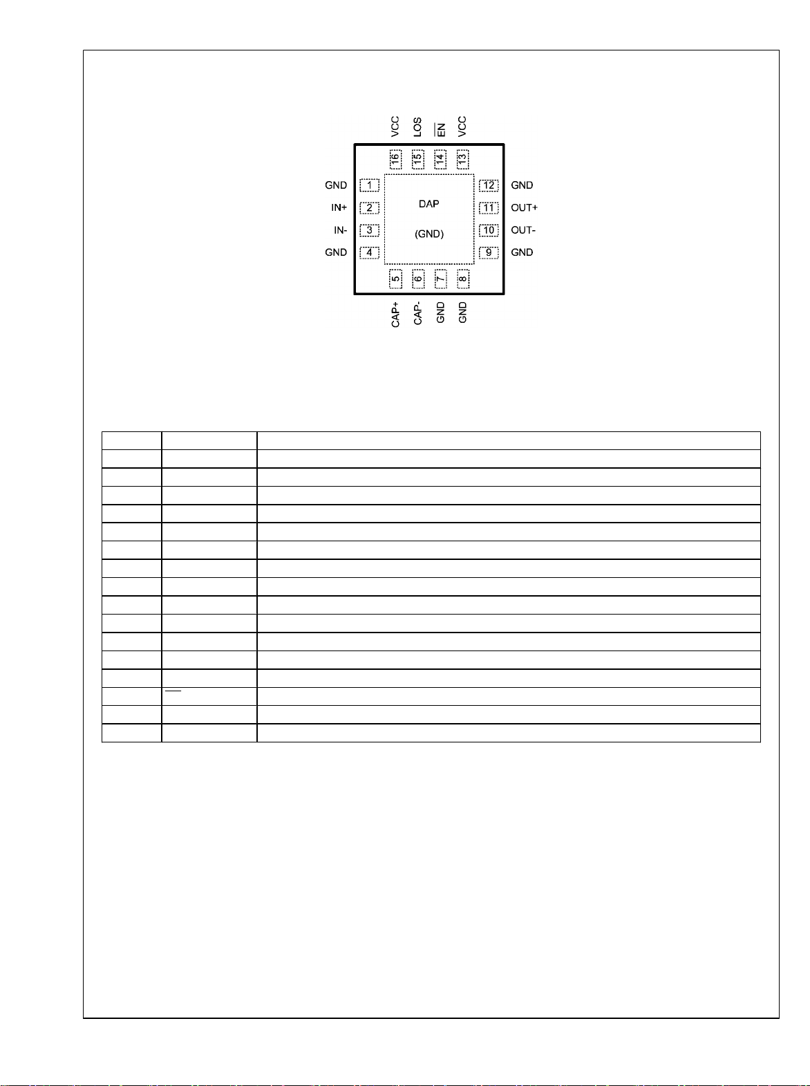
Connection Diagram
DS15EA101
Order Number DS15EA101SQ
See NS Package Number SQA16A
Pin Descriptions
Pin # Name Description
1 GND Ground pin.
2 IN+ Non-inverting input pin.
3 IN- Inverting input pin.
4 GND Ground pin.
5 CAP+ Loop filter positive pin.
6 CAP- Loop filter negative pin.
7 GND Ground pin.
8 GND Ground pin.
9 GND Ground pin.
10 OUT- Inverting output pin.
11 OUT+ Non-inverting output pin.
12 GND Ground pin.
13 VCC Power supply pin.
14 EN Output enable pin.
15 LOS Los of signal circuitry output pin.
16 VCC Power supply pin.
16-Pad LLP
20201703
www.national.com 4
 Loading...