

National Semiconductor COP888xG, COP888xCS Technical data
查询COP684CS供应商
COP888xG/CS Family
8-Bit CMOS ROM Based Microcontrollers with 4k to 24k
Memory, Comparators and USART
General Description
Note: COP8SG devices are form-fit-function compatible su-
persets of the COP888xG/CL/CS Family devices, and are
replacements for these in new designs, and design upgrades with minimum effort.
The COP888xGROM based microcontrollers are highly integrated COP8
to 24k) and advanced features including two Analog comparators. These single-chip CMOS devices are suited for
more complexapplications requiring afull featured controller
with a range of memory sizes, low EMI (except EG), comparators, and a full-duplex USART. Pin and software compatible (different V
™
Feature coredevices with larger memory (4k
range) 8k toor 32k OTP (One Time
CC
July 1999
Programmable) versions are available (COP8SGx7 Family).
Erasable windowed versions are available for use with a
range of software and hardware development tools.
Family features include an 8-bit memory mapped architecture, 10 MHz CKI with 1µs instruction cycle, three multifunction 16-bit timer/counters, full-duplex USART,
MICROWIRE/PLUS
two power saving HALT/IDLE modes, idle timer, MIWU, high
current outputs, software selectable I/O options, WATCH-
™
DOG
timer and Clock Monitor, lowEMI 2.5Vto 5.5Vopera-
tion, and 28/40/44 pin packages.
Devices included in this datasheet are:
™
serial I/O, two Analog comparators,
COP888xG/CS Family, 8-Bit CMOS ROM Based Microcontrollers with 4k to 24k Memory,
Comparators and USART
Device
COP684CS 4k ROM 192 24 28 DIP/SOIC -55 to +125˚C 4.5V - 5.5V
COP884CS 4k ROM 192 24 28 DIP/SOIC -40 to +85˚C
COP984CS 4k ROM 192 24 28 DIP/SOIC -0 to +70˚C 2.5V - 4.0V, CSH=4.0V - 6.0V
COP688CS 4k ROM 192 36/40 40 DIP, 44 PLCC -55 to +125˚C 4.5V - 5.5V
COP888CS 4k ROM 192 36/40 40 DIP, 44 PLCC -40 to +85˚C
COP988CS 4k ROM 192 36/40 40 DIP, 44 PLCC -0 to +70˚C 2.5V - 4.0V, CSH=4.0V - 6.0V
COP884CG 4k ROM 128 24 28 DIP/SOIC -40 to +85˚C 2.5V - 6.0V
COP888CG 4k ROM 128 34/38 40 DIP, 44 PLCC -40 to +85˚C 2.5V - 6.0V
COP684EG 4k ROM 256 24 28 DIP, SOIC -55 to +125˚C 4.5V - 5.5V
COP884EG 4k ROM 256 24 28 DIP, SOIC -40 to +85˚C
COP984EG 4k ROM 256 24 28 DIP, SOIC 0 to +70˚C 2.5V - 4.0V, EGH=4.0 - 6.0V
COP688EG 8k ROM 256 36/40 40 DIP, 44 PLCC -55 to +125˚C 4.5V - 5.5V
COP888EG 8k ROM 256 36/40 40 DIP, 44
COP988EG 8k ROM 256 36/40 40 DIP, 44 PLCC 0 to +70˚C 2.5V - 4.0V, EGH=4.0 - 6.0V
COP688GG 16k ROM 512 36/40 40 DIP, 44
COP888GG 16k ROM 512 36/40 40 DIP, 44
COP688HG 20k ROM 512 36/40 40 DIP, 44 PLCC -55 to +125˚C 4.5V - 5.5V
COP888HG 20k ROM 512 36/40 40 DIP, 44 PLCC -40 to +85˚C
COP688KG 24k ROM 512 36/40 40 DIP, 44 PLCC -55 to +125˚C 4.5V - 5.5V
COP888KG 24k ROM 512 36/40 40 DIP, 44 PLCC -40 to +85˚C
Memory
(bytes)
Key Features
n Full duplex USART
n Three 16-bit timers, each with two 16-bit registers
supporting:
— Processor Independent PWM mode
COP8™, MICROWIRE/PLUS™, and WATCHDOG™are trademarks of National Semiconductor Corporation.
®
TRI-STATE
is a registered trademark of National Semiconductor Corporation.
®
iceMASTER
is a registered trademark of MetaLink Corporation.
© 1999 National Semiconductor Corporation DS012829 www.national.com
RAM
(bytes)
I/O
Pins
Packages Temperature Comments
-40 to +85˚C
PLCC/PQFP
-55 to +125˚C 4.5V - 5.5V
PLCC/PQFP
-40 to +85˚C
PLCC/PQFP
— External Event counter mode
— Input Capture mode
n Quiet design (low radiated emissions)
n 4 to 24 kbytes on-board ROM
n 128 to 512 bytes on-board RAM
Key Features (Continued)
Additional Peripheral Features
n Idle Timer
n Multi-Input Wake-Up (MIWU) with optional interrupts (8)
n Two analog comparators (one for the CS series)
n WATCHDOG and Clock Monitor logic
n MICROWIRE/PLUS serial I/O
I/O Features
n Memory mapped I/O
n Software selectable I/O options (TRI-STATE
Push-Pull Output, Weak Pull-Up Input, High Impedance
Input)
n Up to 8 high current outputs
n Schmitt trigger inputs on ports G and L
n Packages:
— 44 PQFP with 40 I/O pins
— 44 PLCC with 40 I/O pins
— 40 DIP with 36 I/O pins
— 28 DIP/SOIC with 24 I/O pins
®
Output,
CPU/Instruction Set Features
n 1 µs instruction cycle time
n Versatile and easy to use instruction set
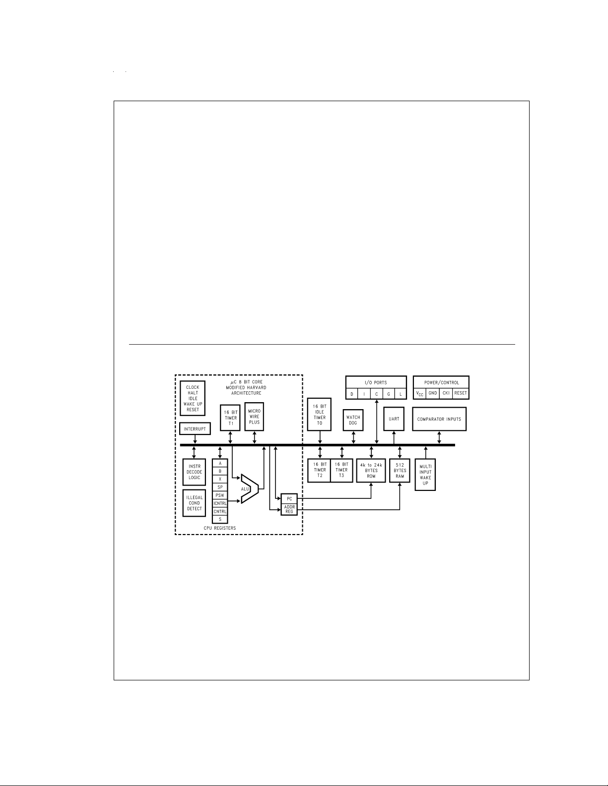
Block Diagram
n Up to fourteen multi-source vectored interrupts servicing
— External Interrupt with selectable edge
— Idle Timer T0
— Three Timers (one timer for the CS series)(each with
2 interrupts)
— MICROWIRE/PLUS
— Multi-Input Wake-Up
— Software Trap
— USART (2)
— Default VIS (default interrupt)
n 8-bit Stack Pointer SP—(stack in RAM)
n Two 8-bit Register Indirect Data Memory Pointers
(B and X)
Fully Static CMOS
n Two power saving modes: HALT and IDLE
n Low current drain (typically
n Single supply operation: 2.5V–5.5V (COP88x)
n Temperature ranges:
0˚C to +70˚C, −40˚C to +85˚C, and −55˚C to +125˚C
<
1 µA)
Development Support
n Emulation and OTP devices
n Real time emulation and full program debug offered by
MetaLink’s Development System
FIGURE 1. COP888xG Block Diagram
www.national.com 2
DS012829-1
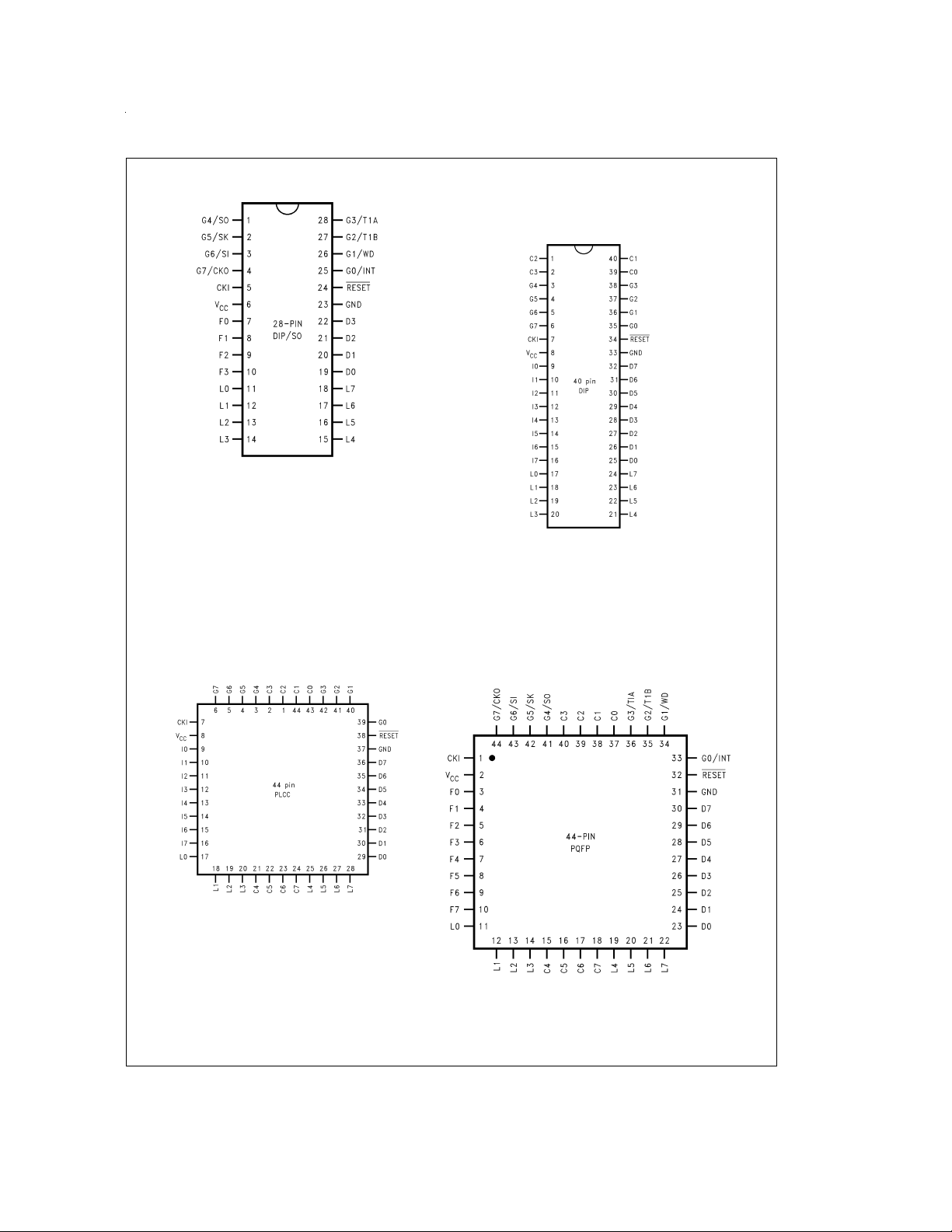
Connection Diagrams
Top View
Order Number COP884CS-XXX/WM,
COP984CS-XXX/WM,
COP984CSH-XXX/WM, COP684CS-XXX/WM,
COP884CG-XXX/WM,
COP884EG-XXX/WM or
COP884CS-XXX/N, COP984CS-XXX/N,
COP984CSH-XXX/N, COP884CG-XXX/N,
COP884EG-XXX/N
See NS Package Number M28B or N28A
Plastic Chip Carrier
Dual-In-Line Package
DS012829-4
DS012829-3
Top View
Order Number COP888CS-XXX/N, COP988CS-XXX/N,
COP688CS-XXX/N,
COP988CSH-XXX/N, COP888CG-XXX/N,
COP688EG-XXX/N, COP888GG-XXX/N,
COP688GG-XXX/N, COP888GG-XXX/N,
COP688HG-XXX/N, COP888HG-XXX/N,
COP688KG-XXX/N, or COP888KG-XXX/N
See NS Package Number N40A
DS012829-2
Top View
Order Number COP688CS-XXX/V, COP888CS-XXX/V,
COP988CS/CSH-XXX/V, COP688EG-XXX/V,
COP888EG-XXX/V, COP988EG-XXX/V,
COP888CG-XXX/V,
COP688GG-XXX/V, COP888GG-XXX/V,
COP688HG-XXX/V, COP888HG-XXX/V,
COP688KG-XXX/V, or COP888KG-XXX/V
See NS Package Number V44A
FIGURE 2. Connection Diagrams
DS012829-43
Top View
Order Number COP888EG-XXX/VEJ,
COP688GG-XXX/VEJ, COP888GG-XXX/VEJ,
See NS Package Number VEJ44A
www.national.com3
Connection Diagrams (Continued)
Pinouts for 28-, 40- and 44-Pin Packages
Port Type Alt. Fun Alt. Fun
L0 I/O MIWU 11 17 17 11
L1 I/O MIWU CKX 12 18 18 12
L2 I/O MIWU TDX 13 19 19 13
L3 I/O MIWU RDX 14 20 20 14
L4 I/O MIWU T2A* 15 21 25 19
L5 I/O MIWU T2B* 16 22 26 20
L6 I/O MIWU T3A* 17 23 27 21
L7 I/O MIWU T3B* 18 24 28 22
G0 I/O INT 25 35 39 33
G1 WDOUT 26 36 40 34
G2 I/O T1B 27 37 41 35
G3 I/O T1A 28 38 42 36
G4 I/O SO 1 3 3 41
G5 I/O SK 2 4 4 42
G6 I SI 3 5 5 43
G7 I/CKO HALT Restart 4 6 6 44
D0O 19252923
D1O 20263024
D2O 21273125
D3O 22283226
D4 O 29 33 7
D5 O 30 34 8
D6 O 31 35 9
D7O 323610
I0 I 7 9 9 27
I1 I COMP1IN− 8 10 10 28
I2 I COMP1IN+ 9 11 11 29
I3 I COMP1OUT 10 12 12 30
I4 I COMP2IN−* 13 13 3
I5 I COMP2IN+* 14 14 4
I6 I COMP2OUT* 15 15 5
I7 I 16 16 6
C0 I/O 39 43 37
C1 I/O 40 44 38
C2 I/O 1 1 39
C3 I/O 2 2 40
C4 I/O 21 15
C5 I/O 22 16
C6 I/O 23 17
C7 I/O 24 18
V
CC
GND 23 33 37 31
CKI 5 7 7 1
RESET
Note 1:*Not available on the CS series
28-Pin 40-Pin 44-Pin 44-Pin
DIP/SO DIP PLCC PQFP
6882
24 34 38 32
www.national.com 4
Absolute Maximum Ratings (Note 4)
If Military/Aerospace specified devices are required,
please contact the National Semiconductor Sales Office/
Distributors for availability and specifications.
Supply Voltage (V
Voltage at Any Pin −0.3V to V
)7V
CC
CC
+ 0.3V
Total Current into V
Pin (Source) 100 mA
CC
Total Current out of GND Pin (Sink) 110 mA
Storage Temperature Range −65˚C to +140˚C
Note 2:
Absolute maximum ratings indicate limits beyond which damage to
the device may occur. DC and AC electrical specifications are not ensured
when operating the device at absolute maximum ratings.
DC Electrical Characteristics 98xEG and 98xCS:
0˚C ≤ TA≤ +70˚C unless otherwise specified
Parameter Conditions Min Typ Max Units
Operating Voltage
COP98xCS, COP98xEG 2.5 4.0 V
COP98xCSH, COP98xEGH 4.0 6.0 V
Power Supply Ripple (Note 6) Peak-to-Peak 0.1 V
Supply Current (Note 7)
CKI=10 MHz V
CKI=4 MHz V
CKI=4 MHz V
CKI=1 MHz V
HALT Current (Note 8) V
=
CC
=
CC
=
CC
=
CC
=
CC
=
V
CC
=
6.0V, t
6.0V, t
4V, t
4V, t
6.0V, CKI=0 MHz
4V, CKI=0 MHz
1 µs 12.5 mA
c
=
2.5 µs 5.5 mA
c
=
2.5 µs 2.5 mA
c
=
10 µs 1.4 mA
c
<
0.7 8 µA
<
0.3 4 µA
IDLE Current
CKI=10 MHz V
CKI=4 MHz V
CKI=1 MHz V
Input Levels (V
IH,VIL
)
=
CC
=
CC
=
CC
=
6.0V, t
6.0V, t
4V, t
1 µs 3.5 mA
c
=
2.5 µs 2.5 mA
c
=
10 µs 0.7 mA
c
RESET
Logic High 0.8 V
CC
Logic Low 0.2 V
CKI (External adn Crystal Osc.
Modes)
Logic High 0.7 V
CC
Logic Low 0.2 V
All Other Inputs
Logic High 0.7 V
CC
Logic Low 0.2 V
Hi-Z Input Leakage V
Input Pullup Current V
=
6.0V, V
CC
=
6.0V, V
CC
=
0V −1 +1 µA
IN
=
0V −40 −250 µA
IN
G and L Port Input Hysteresis (Note 10) 0.35 V
Output Current Levels
D Outputs
Source V
Sink V
=
CC
=
V
CC
=
CC
=
V
CC
4V, V
2.5V, V
4V, V
2.5V, V
=
3.3V −0.4 mA
OH
=
1.8V −0.2 mA
OH
=
1V 10 mA
OL
=
0.4V 2.0 mA
OL
All Others
Source (Weak Pull-Up Mode) V
Source (Push-Pull Mode) V
Sink (Push-Pull Mode) V
=
CC
=
V
CC
=
CC
=
V
CC
=
CC
=
V
CC
4V, V
2.5V, V
4V, V
2.5V, V
4V, V
2.5V, V
=
2.7V −10 −100 µA
OH
=
1.8V −2.5 −33 µA
OH
=
3.3V −0.4 mA
OH
=
1.8V −0.2 mA
OH
=
0.4V 1.6 mA
OL
=
0.4V 0.7 mA
OL
CC
CC
CC
CC
CC
V
V
V
V
V
V
V
V
www.national.com5

DC Electrical Characteristics 98xEG and 98xCS: (Continued)
0˚C ≤ TA≤ +70˚C unless otherwise specified
Parameter Conditions Min Typ Max Units
TRI-STATE Leakage V
=
6.0V −1 +1 µA
CC
Allowable Sink/Source
Current per Pin
D Outputs (Sink) 15 mA
All others 3mA
Maximum Input Current
without Latchup (Notes 9, 10) T
RAM Retention Voltage, V
r
= 25˚
A
500 ns Rise and Fall Time (min) 2 V
±
100 mA
Input Capacitance 7pF
Load Capacitance on D2 1000 pF
AC Electrical Characteristics 98xEG and 98xCS:
0˚C ≤ TA≤ +70˚C unless otherwise specified
Parameter Conditions Min Typ Max Units
Instruction Cycle Time (t
Crystal, Resonator 4V ≤ V
R/C Oscillator 4V ≤ V
Inputs
t
SETUP
t
HOLD
Output Propagation Delay R
t
PD1,tPD0
SO, SK 4V ≤ VCC≤ 6.0V 0.7 µs
All Others 4V ≤ V
MICROWIRE Setup Time (t
MICROWIRE Hold Time (t
MICROWIRE Output Propagation Delay (t
Input Pulse Width (Note 11)
Interrupt Input High Time 1 t
Interrupt Input Low Time 1 t
Timer 1, 2, 3 Input High Time 1 t
Timer 1, 2, 3 Input Low Time 1 t
Reset Pulse Width 1 µs
)
c
2.5V ≤ V
2.5V ≤ V
≤ 6.0V 2.5 DC µs
CC
<
4V 1.0 DC µs
CC
≤ 6.0V 7.5 DC µs
CC
<
4V 3.0 DC µs
CC
4V ≤ VCC≤ 6.0V 200 ns
2.5V ≤ V
<
4V 500 ns
CC
4V ≤ VCC≤ 6.0V 60 ns
2.5V ≤ V
L
2.5V ≤ V
2.5V ≤ V
) (Note 10) 20 ns
UWS
) (Note 10) 56 ns
UWH
) 220 ns
UPD
<
4V 150 ns
CC
=
=
2.2k, C
CC
100 pF
L
<
4V 1.75 µs
CC
≤ 6.0V 1 µs
<
4V 2.5 µs
CC
c
c
c
c
www.national.com 6
Absolute Maximum Ratings (Note 4)
If Military/Aerospace specified devices are required,
please contact the National Semiconductor Sales Office/
Distributors for availability and specifications.
Supply Voltage (V
Voltage at Any Pin −0.3V to V
)7V
CC
CC
+ 0.3V
Total Current into V
Pin (Source) 100 mA
CC
Total Current out of GND Pin (Sink) 110 mA
Storage Temperature Range −65˚C to +140˚C
Note 3:
Absolute maximum ratings indicate limits beyond which damage to
the device may occur. DC and AC electrical specifications are not ensured
when operating the device at absolute maximum ratings.
DC Electrical Characteristics 88xCG, 88xCS, and 88xEG:
−40˚C ≤ TA≤ +85˚C unless otherwise specified
Parameter Conditions Min Typ Max Units
Operating Voltage
Power Supply Ripple (Note 6) Peak-to-Peak 0.1 V
Supply Current (Note 7)
CKI=10 MHz V
CKI=4 MHz V
CKI=4 MHz
(88xCG & 88xEG only)
CKI=1 MHz
(88xCG & 88xEG only)
HALT Current (Note 8) V
(88xCG & 88xEG only) V
=
CC
=
CC
=
V
CC
=
V
CC
=
CC
=
CC
IDLE Current
CKI=10 MHz V
CKI=4 MHz V
CKI=1 MHz
(88xCG & 88xEG only)
Input Levels (V
IH,VIL
)
=
CC
=
CC
=
V
CC
RESET
Logic High 0.8 V
Logic Low 0.2 V
CKI (External adn Crystal Osc.
Modes)
Logic High 0.7 V
Logic Low 0.2 V
All Other Inputs
Logic High 0.7 V
Logic Low 0.2 V
Hi-Z Input Leakage V
Input Pullup Current V
=
CC
=
CC
G and L Port Input Hysteresis (Note 10) 0.35 V
Output Current Levels
D Outputs
Source V
Sink V
=
CC
=
V
CC
=
CC
=
V
CC
All Others
Source (Weak Pull-Up Mode) V
Source (Push-Pull Mode) V
Sink (Push-Pull Mode) V
=
CC
=
V
CC
=
CC
=
V
CC
=
CC
=
6.0V, t
6.0V, t
4V, t
4V, t
6.0V, CKI=0 MHz
4V, CKI=0 MHz
6.0V, t
6.0V, t
4V, t
1 µs 12.5 mA
c
=
2.5 µs 5.5 mA
c
=
2.5 µs 2.5 mA
c
=
10 µs 1.4 mA
c
<
1.0 8 µA
<
0.5 4 µA
=
1 µs 3.5 mA
c
=
2.5 µs 2.5 mA
c
=
10 µs 0.7 mA
c
CC
CC
CC
6.0V −2 +2 µA
6.0V, V
4V, V
2.5V, V
4V, V
2.5V, V
4V, V
2.5V, V
4V, V
2.5V, V
4V, V
=
0V −40 −250 µA
IN
=
3.3V −0.4 mA
OH
=
1.8V −0.2 mA
OH
=
1V 10 mA
OL
=
0.4V 2.0 mA
OL
=
2.7V −10 −100 µA
OH
=
1.8V −2.5 −33 µA
OH
=
3.3V −0.4 mA
OH
=
1.8V −0.2 mA
OH
=
0.4V 1.6 mA
OL
CC
V
V
CC
V
V
CC
V
V
CC
CC
V
V
www.national.com7
DC Electrical Characteristics 88xCG, 88xCS, and 88xEG: (Continued)
−40˚C ≤ TA≤ +85˚C unless otherwise specified
Parameter Conditions Min Typ Max Units
TRI-STATE Leakage V
=
V
2.5V, V
CC
=
6.0V −1 +1 µA
CC
=
0.4V 0.7 mA
OL
Allowable Sink/Source
Current per Pin
D Outputs (Sink) 15 mA
All others 3mA
Maximum Input Current
without Latchup (Notes 9, 10) T
RAM Retention Voltage, V
r
= 25˚
A
500 ns Rise and Fall Time (min) 2 V
±
100 mA
Input Capacitance 7pF
Load Capacitance on D2 1000 pF
AC Electrical Characteristics 888EG, 88xCS, and 88xCG:
−40˚C ≤ TA≤ +85˚C unless otherwise specified
Parameter Conditions Min Typ Max Units
Instruction Cycle Time (t
Crystal, Resonator 4V ≤ V
R/C Oscillator 4V ≤ V
Inputs
t
SETUP
t
HOLD
Output Propagation Delay R
t
PD1,tPD0
SO, SK 4V ≤ VCC≤ 6.0V 0.7 µs
All Others 4V ≤ V
MICROWIRE Setup Time (t
MICROWIRE Hold Time (t
MICROWIRE Output Propagation Delay (t
Input Pulse Width (Note 11)
Interrupt Input High Time 1 t
Interrupt Input Low Time 1 t
Timer 1, 2, 3 Input High Time 1 t
Timer 1, 2, 3 Input Low Time 1 t
Reset Pulse Width 1 µs
)
c
2.5V ≤ V
2.5V ≤ V
≤ 6.0V 1.0 DC µs
CC
<
4V 2.5 DC µs
CC
≤ 6.0V 3.0 DC µs
CC
<
4V 7.5 DC µs
CC
4V ≤ VCC≤ 6.0V 200 ns
2.5V ≤ V
<
4V 500 ns
CC
4V ≤ VCC≤ 6.0V 60 ns
2.5V ≤ V
L
2.5V ≤ V
2.5V ≤ V
) (Note 10) 20 ns
UWS
) (Note 10) 56 ns
UWH
) 220 ns
UPD
<
4V 150 ns
CC
=
=
2.2k, C
CC
100 pF
L
<
4V 1.75 µs
CC
≤ 6.0V 1 µs
<
4V 2.5 µs
CC
c
c
c
c
www.national.com 8
Absolute Maximum Ratings (Note 4)
If Military/Aerospace specified devices are required,
please contact the National Semiconductor Sales Office/
Distributors for availability and specifications.
Supply Voltage (V
Voltage at Any Pin −0.3V to V
)7V
CC
CC
+ 0.3V
Total Current into V
Pin (Source) 100 mA
CC
Total Current out of GND Pin (Sink) 110 mA
Storage Temperature Range −65˚C to +140˚C
Note 4:
Absolute maximum ratings indicate limits beyond which damage to
the device may occur. DC and AC electrical specifications are not ensured
when operating the device at absolute maximum ratings.
DC Electrical Characteristics 888GG, 888HG, and 888KG:
−40˚C ≤ TA≤ +85˚C unless otherwise specified
Parameter Conditions Min Typ Max Units
Operating Voltage 2.5 5.5 V
Power Supply Ripple (Note 6) Peak-to-Peak 0.1 V
CC
Supply Current (Note 7)
CKI=10 MHz V
CKI=4 MHz V
CKI=4 MHz V
CKI=1 MHz V
HALT Current (Note 8) V
=
CC
=
CC
=
CC
=
CC
=
CC
=
V
CC
=
5.5V, t
5.5V, t
4V, t
4V, t
5.5V, CKI=0 MHz
4V, CKI=0 MHz
1 µs 12.5 mA
c
=
2.5 µs 5.5 mA
c
=
2.5 µs 2.5 mA
c
=
10 µs 1.4 mA
c
<
110 µA
<
0.5 6 µA
IDLE Current
CKI=10 MHz V
CKI=4 MHz V
CKI=1 MHz V
Input Levels (V
IH,VIL
)
=
CC
=
CC
=
CC
=
5.5V, t
5.5V, t
4V, t
1 µs 3.5 mA
c
=
2.5 µs 2.5 mA
c
=
10 µs 0.7 mA
c
RESET
Logic High 0.8 V
Logic Low 0.2 V
CC
CC
CKI, All Other Inputs
Logic High 0.7 V
Logic Low 0.2 V
Hi-Z Input Leakage V
Input Pullup Current V
=
5.5V, V
CC
=
5.5V, V
CC
=
0V −2 +2 µA
IN
=
0V −40 −250 µA
IN
G and L Port Input Hysteresis (Note 10) 0.35 V
CC
CC
CC
Output Current Levels
D Outputs
Source V
Sink V
=
CC
=
V
CC
=
CC
=
V
CC
4V, V
2.5V, V
4V, V
2.5V, V
=
3.3V −0.4 mA
OH
=
1.8V −0.2 mA
OH
=
1V 10 mA
OL
=
0.4V 2.0 mA
OL
All Others
Source (Weak Pull-Up Mode) V
Source (Push-Pull Mode) V
Sink (Push-Pull Mode) V
TRI-STATE Leakage V
=
CC
=
V
CC
=
CC
=
V
CC
=
CC
=
V
CC
=
CC
=
4V, V
2.5V, V
4V, V
2.5V, V
4V, V
2.5V, V
2.7V −10 −100 µA
OH
=
1.8V −2.5 −33 µA
OH
=
3.3V −0.4 mA
OH
=
1.8V −0.2 mA
OH
=
0.4V 1.6 mA
OL
=
0.4V 0.7 mA
OL
5.5V −2 +2 µA
Allowable Sink/Source
Current per Pin
D Outputs (Sink) 15 mA
All others 3mA
Maximum Input Current
V
V
V
V
V
V
www.national.com9
DC Electrical Characteristics 888GG, 888HG, and 888KG: (Continued)
−40˚C ≤ TA≤ +85˚C unless otherwise specified
Parameter Conditions Min Typ Max Units
±
without Latchup (Notes 9, 10) Room Temperature
RAM Retention Voltage, V
r
500 ns Rise and Fall Time (min) 2 V
100 mA
Input Capacitance 7pF
Load Capacitance on D2 (Note 10) 1000 pF
AC Electrical Characteristics 888GG, 888HG, and 888KG:
−40˚C ≤ TA≤ +85˚C unless otherwise specified
Parameter
(88xCG & 88xEG only)
Instruction Cycle Time (t
)
c
Crystal, Resonator 2.5V ≤ V
R/C Oscillator 2.5V ≤ V
Inputs
t
SETUP
t
HOLD
Output Propagation Delay R
t
PD1,tPD0
SO, SK 4V ≤ VCC≤ 5.5V 0.7 µs
All Others 4V ≤ V
MICROWIRE Setup Time (t
MICROWIRE Hold Time (t
MICROWIRE Output Propagation Delay (t
) (Note 10) VCC≥ 4V 20 ns
UWS
) (Note 10) VCC≥ 4V 56 ns
UWH
)VCC≥ 4V 220 ns
UPD
Input Pulse Width (Note 11)
Interrupt Input High Time 1 t
Interrupt Input Low Time 1 t
Timer 1, 2, 3 Input High Time 1 t
Timer 1, 2, 3 Input Low Time 1 t
Reset Pulse Width 1 µs
Conditions Min Typ Max Units
<
4V 1.0 DC µs
CC
4V ≤ V
4V ≤ V
≤ 5.5V 2.5 DC µs
CC
<
4V 3.0 DC µs
CC
≤ 5.5V 7.5 DC µs
CC
4V ≤ VCC≤ 5.5V 200 ns
2.5V ≤ V
<
4V 500 ns
CC
4V ≤ VCC≤ 5.5V 60 ns
2.5V ≤ V
L
2.5V ≤ V
2.5V ≤ V
<
4V 150 ns
CC
=
=
2.2k, C
CC
100 pF
L
<
4V 1.75 µs
CC
≤ 5.5V 1 µs
<
4V 2.5 µs
CC
c
c
c
c
www.national.com 10
Absolute Maximum Ratings (Note 5)
If Military/Aerospace specified devices are required,
please contact the National Semiconductor Sales Office/
Distributors for availability and specifications.
Supply Voltage (V
Voltage at Any Pin −0.3V to V
)7V
CC
CC
+ 0.3V
Total Current into V
Pin (Source) 100 mA
CC
Total Current out of GND Pin (Sink) 110 mA
Storage Temperature Range −65˚C to +140˚C
Note 5:
Absolute maximum ratings indicate limits beyond which damage to
the device may occur. DC and AC electrical specifications are not ensured
when operating the device at absolute maximum ratings.
DC Electrical Characteristics 68xCS and 68xxG:
−55˚C ≤ TA≤ +125˚C unless otherwise specified
Parameter Conditions Min Typ Max Units
Operating Voltage 4.5 5.5 V
Power Supply Ripple (Note 6) Peak-to-Peak 0.1 V
Supply Current (Note 7)
CKI=10 MHz V
CKI=4 MHz V
HALT Current (Note 8) V
=
CC
=
CC
=
CC
=
5.5V, t
5.5V, t
1 µs 12.5 mA
c
=
2.5 µs 5.5 mA
c
5.5V, CKI=0 MHz
<
10 30 µA
IDLE Current
CKI=10 MHz V
CKI=4 MHz V
Input Levels (V
IH,VIL
)
=
CC
=
CC
5.5V, t
5.5V, t
=
1 µs 3.5 mA
c
=
2.5 µs 2.5 mA
c
RESET
Logic High 0.8 V
CC
Logic Low 0.2 V
CKI (68xCS & 68xEG only)
Logic High 0.7 V
CC
Logic Low 0.2 V
All Other Inputs
Logic High 0.7 V
CC
Logic Low 0.2 V
Hi-Z Input Leakage V
Input Pullup Current V
=
5.5V, V
CC
=
5.5V, V
CC
=
0V −5 +5 µA
IN
=
0V −35 −400 µA
IN
G and L Port Input Hysteresis (Note 10) 0.35 V
Output Current Levels
D Outputs
Source V
Sink V
=
4.5V, V
CC
=
4.5V, V
CC
=
3.3V −0.4 mA
OH
=
1V 9 mA
OL
All Others
Source (Weak Pull-Up Mode) V
Source (Push-Pull Mode) V
Sink (Push-Pull Mode) V
TRI-STATE Leakage V
=
4.5V, V
CC
=
4.5V, V
CC
=
4.5V, V
CC
=
5.5V −5 +5 µA
CC
=
2.7V −9 −140 µA
OH
=
3.3V −0.4 mA
OH
=
0.4V 1.4 mA
OL
Allowable Sink/Source
Current per Pin
D Outputs (Sink) 12 mA
All others 2.5 mA
Maximum Input Current
without Latchup (Notes 9, 10) Room Temp
RAM Retention Voltage, V
r
500 ns Rise and Fall Time (min) 2 V
Input Capacitance (Note 10) 7 pF
Load Capacitance on D2 (Note 10) 1000 pF
CC
CC
CC
CC
CC
±
100 mA
V
V
V
V
V
V
V
V
www.national.com11
AC Electrical Characteristics 68xCS and 68xxG:
−55˚C ≤ TA≤ +125˚C unless otherwise specified
Parameter Conditions Min Typ Max Units
Instruction Cycle Time (t
Crystal, Resonator V
R/C Oscillator
68xCS & 68xEG only)
Inputs
t
SETUP
t
HOLD
Output Propagation Delay R
t
PD1,tPD0
SO, SK VCC≥ 4.5V 0.7 µs
All Others V
MICROWIRE
™
MICROWIRE Hold Time (t
MICROWIRE Output Propagation Delay (t
Input Pulse Width (Note 11)
Interrupt Input High Time 1 t
Interrupt Input Low Time 1 t
Timer 1, 2, 3 Input High Time 1 t
Timer 1, 2, 3 Input Low Time 1 t
Reset Pulse Width 1 µs
Note 6: Maximum rate of voltage change must be less than 0.5 V/ms.
Note 7: Supply current is measured after running 2000 cycles with a square wave CKI input, CKO open, inputs at rails and outputs open.
Note 8: The HALT mode will stop CKI from oscillating in the RC and the Crystal configurations. Measurement of IDD HALTis done with device neither sourcing or
sinking current; with L, C, and G0–G5 programmed as low outputs and not driving a load; all outputs programmed low and not driving a load; all inputs tied to V
clock monitor and comparatorsdisabled. Parameter refers toHALTmode entered via setting bit 7 of theG Port data register.Partwill pull up CKIduring HALTin crystal clock mode.
Note 9: Pins G6 and RESET are designed with a high voltage input network. These pins allow input voltages greater than V
to VCCwhen biased atvoltages greater thanVCC(the pins donot have sourcecurrent when biasedat a voltagebelow VCC). The effective resistance to VCCis 750Ω
(typical). These two pins will not latch up. The voltage at the pins must be limited to less than 14V. WARNING: Voltagesin excess of 14V will cause damage to the
pins. This warning excludes ESD transients.
Note 10: Parameter characterized but not tested.
Note 11: t
=
Instruction Cycle Time
c
)
c
Setup Time (t
UWH
≥ 4.5V 1.0 DC µs
CC
V
≥ 4.5V 3.0 DC µs
CC
VCC≥ 4.5V 200 ns
VCC≥ 4.5V 60 ns
=
L
≥ 4.5V 1 µs
) (Note 10) 20 ns
UWS
CC
2.2k, C
L
=
100 pF
) (Note 10) 56 ns
) 220 ns
UPD
and the pins will have sink current
CC
c
c
c
c
;
CC
Comparators AC and DC Characteristics
=
V
5V, −40˚C ≤ T
CC
Input Offset Voltage 0.4V ≤ V
Input Common Mode Voltage Range 0.4 V
Voltage Gain 300k V/V
Low Level Output Current V
High Level Output Current V
DC Supply Current per Comparator (When Enabled) 250 µA
Response Time 100 mV Overdrive, 1 µs
www.national.com 12
≤ +85˚C.
A
Parameter Conditions Min Typ Max Units
≤ VCC− 1.5V
IN
=
0.4V 1.6 mA
OL
=
4.6V 1.6 mA
OH
±
10
±
25 mV
− 1.5 V
CC
100 pF Load
Comparators AC and DC Characteristics (Continued)
DS012829-4
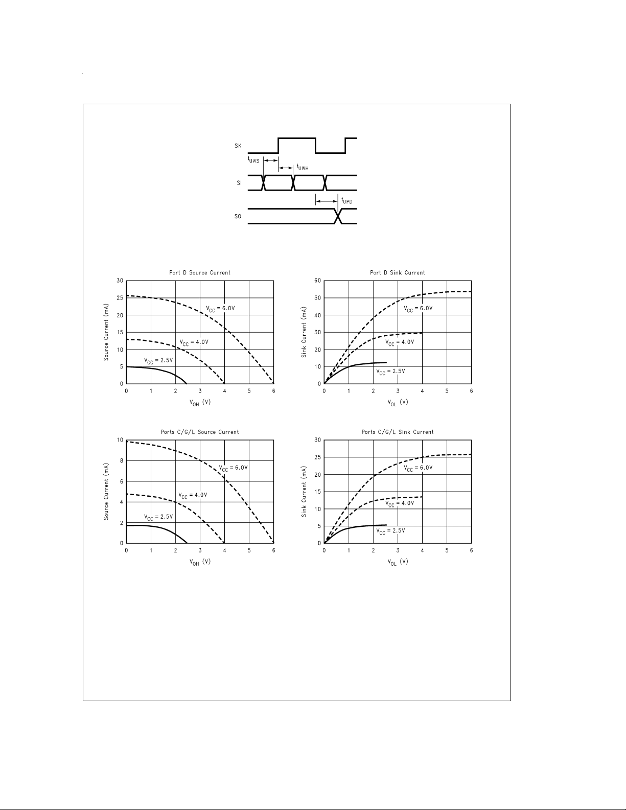
FIGURE 3. MICROWIRE/PLUS Timing
Typical Performance Characteristics (−55˚C ≤ T
DS012829-30 DS012829-31
A
=
+125˚C)
DS012829-32 DS012829-33
www.national.com13
Typical Performance Characteristics (−55˚C ≤ T
=
+125˚C) (Continued)
A
DS012829-34
DS012829-36 DS012829-37
DS012829-35
DS012829-38 DS012829-39
www.national.com 14
Typical Performance Characteristics (−55˚C ≤ T
=
+125˚C) (Continued)
A
DS012829-40
Pin Descriptions
VCCand GND are the power supply pins. All VCCand GND
pins must be connected.
CKI isthe clock input. This can come from an R/C generated
oscillator, or a crystal oscillator (in conjunction with CKO).
See Oscillator Description section.
RESET is the master reset input.See ResetDescription section.
The device contains three bidirectional 8-bit I/O ports (C, G
and L), where each individual bit may be independently configured asan input (SchmittTrigger inputs on ports L and G),
output or TRI-STATE under program control. Three data
memory address locations are allocated for each of these
I/O ports. Each I/O port has two associated 8-bit memory
mapped registers, the CONFIGURATION register and the
output DATAregister. A memory mapped address is also reserved for the input pins of each I/O port. (See the memory
map for the various addresses associatedwith theI/O ports.)
Figure 4
shows the I/O port configurations. The DATA and
CONFIGURATION registers allow for each port bit to be individually configured under software control as shown below:
CONFIGURATION DATA Port Set-Up
Register Register
0 0 Hi-Z Input
0 1 Input with Weak Pull-Up
1 0 Push-Pull Zero Output
1 1 Push-Pull One Output
PORT L is an 8-bit I/O port. All L-pins have Schmitt triggers
on the inputs.
The Port L supports Multi-Input WakeUp on all eight pins. L1
is used for the USART external clock. L2 andL3 are used for
the USARTtransmit and receive. L4 and L5 are used for the
timer input functions T2A and T2B. L6 and L7 are used for
the timer input functions T3Aand T3B (execpt on the CS series).
The Port L has the following alternate features:
L7 MIWU or T3B
L6 MIWU or T3A
L5 MIWU or T2B
L4 MIWU or T2A
L3 MIWU or RDX
(TRI-STATE Output)
DS012829-41
L2 MIWU or TDX
L1 MIWU or CKX
L0 MIWU
Port G is an 8-bit port with 5 I/O pins (G0, G2–G5), an input
pin (G6), and a dedicated output pin (G1). Pins G0 and
G2–G6 all have Schmitt Triggers on their inputs. Pin G1
serves as the dedicated WDOUT WATCHDOG output, while
pin G7 is either input or output depending on the oscillator
mask option selected. With the crystal oscillator option selected, G7 serves as the dedicated output pin for the CKO
clock output. With the single-pin R/C oscillator mask option
selected, G7 serves as a general purpose input pin but is
also used to bring the device out of HALT mode with a low to
high transition on G7. There are two registers associated
with the G Port, a data register and a configuration register.
Therefore, each of the 5 I/O bits (G0, G2–G5) can be individually configured under software control.
Since G6 is an input only pin and G7 is the dedicated CKO
clock output pin (crystal clock option) or general purpose input (R/C clock option), the associated bits in the data and
configuration registers for G6 and G7 are used for special
purpose functions as outlined on the next page. Reading the
G6 and G7 data bits will return zeros.
DS012829-5
FIGURE 4. I/O Port Configurations
Note thatthe chip will be placed in the HALT mode by writing
a “1” to bit 7 of the Port G Data Register. Similarly the chip
will beplaced in theIDLE mode by writing a “1” to bit 6 of the
Port G Data Register.
Writing a “1” to bit 6 of the Port G Configuration Register enables the MICROWIRE/PLUS to operate with the alternate
www.national.com15
Pin Descriptions (Continued)
phase of the SK clock. The G7 configuration bit, if set high,
enables the clock start up delay after HALT when the R/C
clock configuration is used.
Config Reg. Data Reg.
G7 CLKDLY HALT
G6 Alternate SK IDLE
Port G has the following alternate features:
G6 SI (MICROWIRE Serial Data Input)
G5 SK (MICROWIRE Serial Clock)
G4 SO (MICROWIRE Serial Data Output)
G3 T1A (Timer T1 I/O)
G2 T1B (Timer T1 Capture Input)
G0 INTR (External Interrupt Input)
Port G has the following dedicated functions:
G7 CKO Oscillator dedicated output or general purpose
input
G1 WDOUT WATCHDOG and/or Clock Monitor dedi-
cated output
Port C is an 8-bit I/O port. The 40-pin device does not have
a full complement of Port C pins. The unavailable pins are
not terminated.A read operation for these unterminated pins
will return unpredicatable values.
Port I is an eight-bit Hi-Z input port.
Port I1–I3 are used forComparator 1.Port I4–I6 are used for
Comparator 2.
The Port I has the following alternate features:
I6 COMP2OUT (Comparator 2 Output)
I5 COMP2+IN (Comparator 2 Positive Input)
I4 COMP2−IN (Comparator 2 Negative Input)
I3 COMP1OUT (Comparator 1 Output)
I2 COMP1+IN (Comparator 1 Positive Input)
I1 COMP1−IN (Comparator 1 Negative Input)
Port D is an 8-bit output port that ispreset high when RESET
goes low. The user can tie two or more D port outputs (except D2) together in order to get a higher drive.
Functional Description
The architecture of the device is modified Harvard architecture. With the Harvard architecture, the control store program memory (ROM) is separated from the data store
memory (RAM). Both ROM and RAM have their own separate addressing space with separate address buses.The architecture, though based on Harvard architecture, permits
transfer of data from ROM to RAM.
CPU REGISTERS
The CPU can doan 8-bit addition, subtraction, logicalor shift
operation in one instruction (t
There are six CPU registers:
A is the 8-bit Accumulator Register
PC is the 15-bit Program Counter Register
PU is the upper 7 bits of the program counter (PC)
PL is the lower 8 bits of the program counter (PC)
B is an 8-bit RAM address pointer, which can be optionally
post auto incremented or decremented.
X is an 8-bit alternate RAM address pointer, which can be
optionally post auto incremented or decremented.
www.national.com 16
) cycle time.
c
SP is the 8-bit stack pointer, which points to the subroutine/
interrupt stack (in RAM). The SP is initialized to RAM address 06F with reset.
S is the 8-bitData SegmentAddress Register used to extend
the lower half of the address range (00 to 7F) into 256 data
segments of 128 bytes each.
All the CPU registers are memory mapped with the exception of the Accumulator (A) and the Program Counter (PC).
PROGRAM MEMORY
The program memory consists of up to 24 kbytes of ROM.
These bytes may hold program instructions or constant data
(data tablesfor the LAIDinstruction, jump vectors for the JID
instruction, and interrupt vectors for the VIS instruction). The
program memory is addressed by the 15-bit program
counter (PC). All interrupts in the devices vector to program
memory location 0FF Hex.
DATA MEMORY
The data memory address space includes the on-chip RAM
and data registers, theI/O registers (Configuration, Data and
Pin), the control registers, the MICROWIRE/PLUS SIO shift
register, and the various registers, and counters associated
with the timers (with the exception of the IDLE timer). Data
memory is addressed directly by the instruction or indirectly
by the B, X, SP pointers and S register.
The data memory consists of up to 512 bytes of RAM. Sixteen bytes of RAM are mapped as “registers” at addresses
0F0 to0FF Hex. These registers can be loaded immediately,
and also decremented and tested withthe DRSZ(decrement
register and skip if zero) instruction. The memory pointer
registers X,SP,B and S are memorymapped into thisspace
at address locations 0FC to 0FF Hex respectively, with the
other registers being available for general usage.
The instructionset permits anybit in memoryto be set,reset
or tested. All I/O and registers (except A and PC) are
memory mapped; therefore, I/O bits and register bits can be
directly andindividually set, reset and tested. The accumulator (A) bits can also be directly and individually tested.
Note: RAM contents are undefined upon power-up.
Data Memory Segment RAM
Extension
Data memory address 0FF is used as a memory mapped location for the Data Segment Address Register (S).
The data store memory is either addressed directly by a
single byte address within the instruction, or indirectly relative to the reference of the B, X, or SP pointers (each contains a single-byte address). This single-byte address allows
an addressingrange of 256 locations from 00 to FF hex. The
upper bit of this single-byte address divides the data store
memory into two separate sections as outlined previously.
With the exception of the RAM register memory from address locations 00F0 to 00FF, all RAM memory is memory
mapped with the upper bit of the single-byte address being
equal to zero. This allows the upper bit of the single-byte address to determine whether or not the base address range
(from 0000 to 00FF) is extended. If this upper bit equals one
(representing address range 0080 to 00FF), then address
extension does not take place. Alternatively, if this upper bit
equals zero, then the data segment extension register S is
used to extend the base address range (from 0000 to 007F)
from XX00 to XX7F,where XX represents the 8 bits from the
S register. Thus the 128-byte data segment extensions are
located from addresses 0100 to 017F for data segment 1,
 Loading...