


查询COP684EK供应商
COP888EK
8-Bit CMOS ROM Based Microcontrollers with 8k
Memory, Comparator, and Single-slope A/D Capability
OBSOLETE
January 2000
COP888EK 8-Bit CMOS ROM Based Microcontrollers with 8k Memory, Comparator, and
Single-slope A/D Capability
General Description
The COP888EK ROM based microcontrollers are highly integrated COP8
advanced features including a Multi-Input Comparator and
Single-slope A/D capability. These single-chip CMOS devices are suited for applications requiring a full featured, low
EMI controller with an analog comparator, current source,
and voltage reference. The COP87L88EK/RK Family devices are pin and software compatible (different V
16k or 32k OTP (One Time Programmable) versions for preproduction, and for use with a range of COP8 software and
hardware development tools.
Device Memory (bytes) RAM (bytes) I/O Pins Packages Temperature Comments
COP684EK 8k ROM 256 24 28 DIP/SOIC -55 to +125˚C 4.5V - 5.5V
COP884EK 8k ROM 256 24 28 DIP/SOIC -40 to +85˚C
COP984EK 8k ROM 256 24 28 DIP/SOIC 0 to +70˚C 2.5V - 4.0V, EKH=4.0V - 6.0V
COP688EK 8k ROM 256 36/40 40 DIP, 44 PLCC -55 to +125˚C 4.5V - 5.5V
COP888EK 8k ROM 256 36/40 40 DIP, 44 PLCC -40 to +85˚C
COP988EK 8k ROM 256 36/40 40 DIP, 44 PLCC 0 to +70˚C 2.5V - 4.0V, EKH=4.0V - 6.0V
™
Feature core devices with 8k memory and
CC
range)
Key Features
n Analog function block with
— Analog comparator with seven input multiplexor
— Constant current source and V
n Three 16-bit timers, each with two 16-bit registers
supporting:
— Processor Independent PWM mode
— External Event counter mode
— Input Capture mode
n 8 kbytes of on-chip ROM
n 256 bytes of on-chip RAM
/2 reference
CC
Additional Peripheral Features
n Idle Timer
n Multi-Input Wake Up (MIWU) with optional interrupts (8)
n WATCHDOG and Clock Monitor logic
n MICROWIRE/PLUS serial I/O
I/O Features
n Software selectable I/O options (TRI-STATE™Output,
Push-Pull Output, Weak Pull-Up Input, High Impedance
Input)
n High current outputs
n Schmitt trigger inputs on Port G and L
n Packages: 44 PLCC with 40 I/O pins, 40 DIP with 36 I/O
pins, and 28 DIP/SO with 24 I/O pins
Family features include an 8-bit memory mapped architecture, 10 MHz CKI with 1µs instruction cycle, three multifunction 16-bit timer/counters with PWM, MICROWIRE/
™
PLUS
multiplexor, an analog current source and V
two power saving HALT/IDLE modes, idle timer, MIWU, high
current outputs, software selectable I/O options, WATCHDOG
eration and 28/40/44 pin packages.
Devices included in this datasheet are:
serial I/O, one analog comparator with seven input
reference,
CC
™
timer and Clock Monitor, Low EMI 2.5V to 6.0V op-
CPU/Instruction Set Feature
n 1 µs instruction cycle time
n Twelve multi-source vectored interrupts servicing
— External Interrupt with selectable edge
— Idle Timer T0
— Three Timers (Each with 2 interrupts)
— MICROWIRE/PLUS
— Multi-Input Wake Up
— Software Trap
— Default VIS (default interrupt)
n Versatile and easy to use instruction set
n 8-bit Stack Pointer (SP)—stack in RAM
n Two 8-bit Register Indirect Data Memory Pointers
(B, X)
Fully Static CMOS
n Single supply operation: 2.5V to 6.0V
n Temperature ranges: 0˚C to +70˚C, −40˚C to +85˚C, and
−55˚C to +125˚C
COP8™, MICROWIRE/PLUS™, and WATCHDOG™are trademarks of National Semiconductor Corporation.
®
TRI-STATE
iceMASTER
© 2000 National Semiconductor Corporation DS012094 www.national.com
is a registered trademark of National Semiconductor Corporation.
®
is a registered trademark of MetaLink Corporation.
Development Support
n Emulation and OTP devices
COP888EK
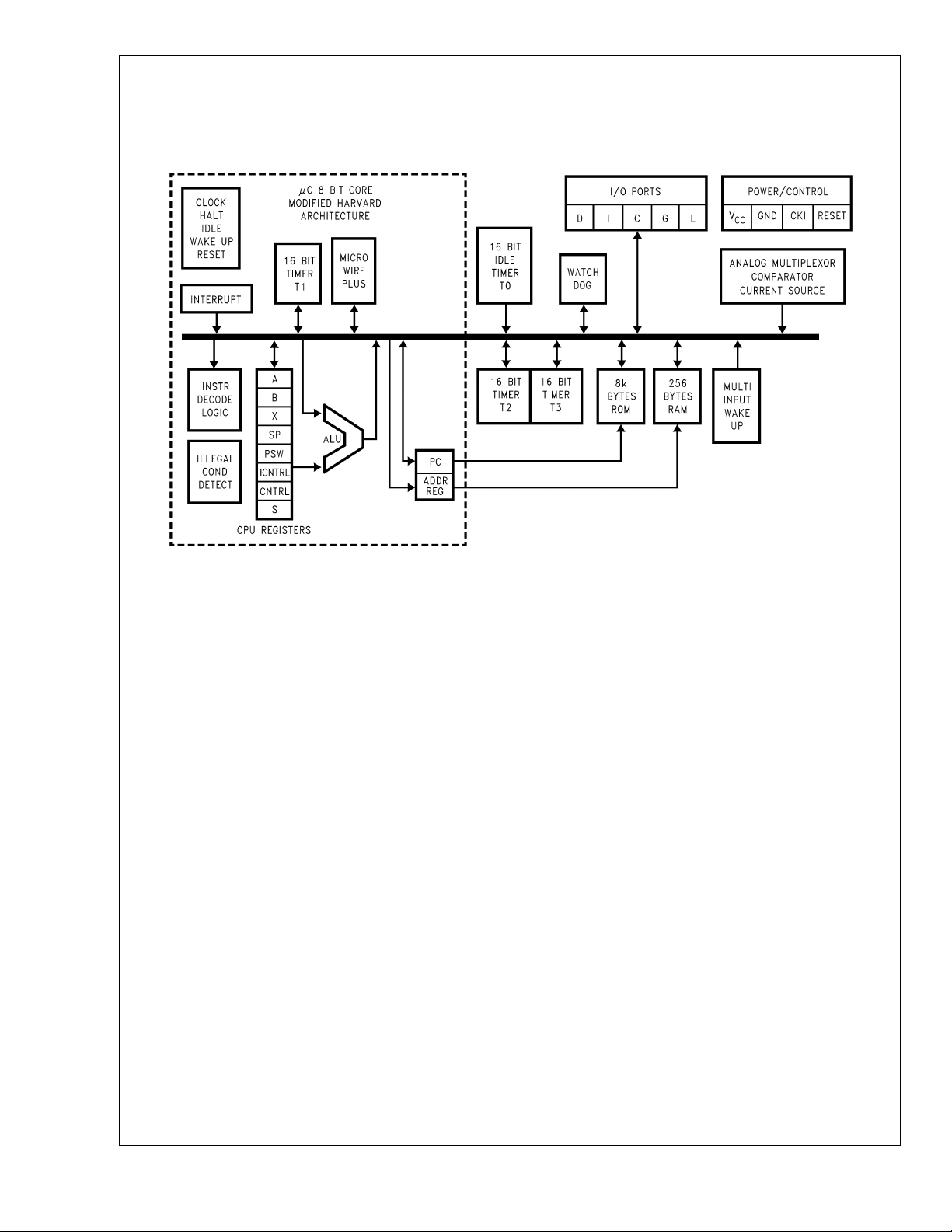
Block Diagram
n Real time emulation and full program debug offered by
MetaLink Development System
FIGURE 1. Block Diagram
DS012094-1
www.national.com 2
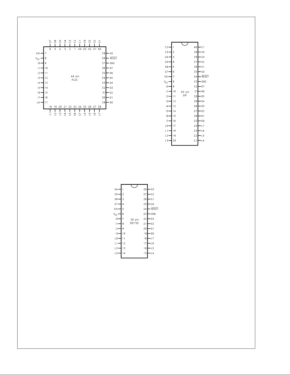
Connection Diagrams
COP888EK
Plastic Chip Carrier
DS012094-2
Top View
Order Number COP688EK-XXX/V, COP888EK-XXX/V,
COP988EK-XXX/V or COP988EKH-XXX/V
See NS Plastic Chip Package Number V44A
Dual-In-Line Package
DS012094-3
Top View
Order Number COP688EK-XXX/N, COP888EK-XXX/N,
COP988EK-XXX/N or COP988EKH-XXX/N
See NS Molded Package Number N40A
Dual-In-Line Package
DS012094-4
Top View
Order Number COP684EK-XXX/N, COP884EK-XXX/N, COP984EK-XXX/N or COP984EKH-XXX/N
See NS Molded Package Number N28B
Order Number COP684EK-XXX/WM, COP884EK-XXX/WM, COP984EK-XXX/WM or COP984EKH-XXX/WM
See NS Molded Package Number M28B
FIGURE 2. Connection Diagrams
www.national.com3
Connection Diagrams (Continued)
Pinouts for 28-, 40- and 44-Pin Packages
COP888EK
Port Type Alt. Fun Alt. Fun
L0 I/O MIWU 11 17 17
L1 I/O MIWU 12 18 18
L2 I/O MIWU 13 19 19
L3 I/O MIWU 14 20 20
L4 I/O MIWU T2A 15 21 25
L5 I/O MIWU T2B 16 22 26
L6 I/O MIWU T3A 17 23 27
L7 I/O MIWU T3B 18 24 28
G0 I/O INT 25 35 39
G1 WDOUT 26 36 40
G2 I/O T1B 27 37 41
G3 I/O T1A 28 38 42
G4 I/O SO 1 3 3
G5 I/O SK 2 4 4
G6ISI 355
G7 I/CKO HALT Restart 4 6 6
D0O 192529
D1O 202630
D2O 212731
D3O 222832
I0 I COMPIN1+ 7 9 9
I1 I COMPIN−/Current 8 10 10
Source Out
I2 I COMPIN0+ 9 11 11
I3 I COMPOUT/COMPIN2+ 10 12 12
I4 I COMPIN3+ 13 13
I5 I COMPIN4+ 14 14
I6 I COMPIN5+ 15 15
I7 I COMPOUT 16 16
D4 O 29 33
D5 O 30 34
D6 O 31 35
D7 O 32 36
C0 I/O 39 43
C1 I/O 40 44
C2 I/O 1 1
C3 I/O 2 2
C4 I/O 21
C5 I/O 22
C6 I/O 23
C7 I/O 24
V
CC
GND 23 33 37
CKI 5 7 7
RESET
28-Pin 40-Pin 44-Pin
Pack. Pack. Pack.
688
24 34 38
www.national.com 4
COP888EK
Absolute Maximum Ratings (Note 1)
If Military/Aerospace specified devices are required,
please contact the National Semiconductor Sales Office/
Distributors for availability and specifications.
Supply Voltage (V
Voltage at Any Pin −0.3V to V
)7V
CC
+ 0.3V
CC
Total Current into V
Total Current out of GND Pin (Sink) 110 mA
Storage Temperature Range −65˚C to +140˚C
Note 1:
Absolute maximum ratings indicate limits beyond which damage to
the device may occur. DC and AC electrical specifications are not ensured
when operating the device at absolute maximum ratings.
Pin (Source) 100 mA
CC
DC Electrical Characteristics 98xEK:
0˚C ≤ TA≤ + 70˚C unless otherwise specified
Parameter Conditions Min Typ Max Units
Operating Voltage COP98XEK 2.5 4.0 V
COP98XEKH 4.0 6.0 V
Power Supply Ripple (Note 3) Peak-to-Peak 0.1 V
CC
Supply Current (Note 4)
CKI=10 MHz V
CKI=4 MHz V
HALT Current (Note 5) V
=
6.0V, t
CC
=
2.5V, t
CC
=
6.0V, CKI=0 MHz
CC
=
V
4.0V, CKI=0 MHz
CC
=
1 µs 10.0 mA
c
=
2.5 µs 1.7 mA
c
<
48 µA
<
34 µA
IDLE Current (Note 4)
CKI=10 MHz V
CKI=4 MHz V
Input Levels (V
IH,VIL
)
=
6.0V, t
CC
=
2.5V, t
CC
=
1 µs 0.4 1.7 mA
c
=
2.5 µs 0.2 0.5 mA
c
RESET
Logic High 0.8 V
Logic Low 0.2 V
CC
CC
CKI, All Other Inputs
Logic High 0.7 V
Logic Low 0.2 V
Hi-Z Input Leakage V
Input Pullup Current V
=
6.0V −1 +1 µA
CC
=
6.0V, V
CC
=
0V −40 −250 µA
IN
G and L Port Input Hysteresis (Note 8) 0.35 V
CC
CC
CC
Output Current Levels
D Outputs
Source V
Sink V
=
4.0V, V
CC
=
V
2.5V, V
CC
=
4.0V, V
CC
=
V
2.5V, V
CC
=
3.3V −0.4 mA
OH
=
1.8V −0.2 mA
OH
=
1V 10 mA
OL
=
0.4V 2.0 mA
OL
All Others
Source (Weak Pull-Up Mode) V
Source (Push-Pull Mode) V
Sink (Push-Pull Mode) V
TRI-STATE Leakage V
=
4.0V, V
CC
=
V
2.5V, V
CC
=
4.0V, V
CC
=
V
2.5V, V
CC
=
4.0V, V
CC
=
V
2.5V, V
CC
=
6.0V −1 +1 µA
CC
=
2.7V −10 −110 µA
OH
=
1.8V −2.5 −33 µA
OH
=
3.3V −0.4 mA
OH
=
1.8V −0.2 mA
OH
=
0.4V 1.6 mA
OL
=
0.4V 0.7 mA
OL
Allowable Sink/Source Current per Pin
(Note 8)
D Outputs (Sink) 15 mA
All others 3mA
Maximum Input Current Room Temp
±
100 mA
without Latchup (Note 6)
RAM Retention Voltage, V
r
500 ns Rise and Fall Time (Min) 2 V
V
V
V
V
V
V
www.national.com5
DC Electrical Characteristics 98xEK: (Continued)
0˚C ≤ TA≤ + 70˚C unless otherwise specified
COP888EK
Parameter Conditions Min Typ Max Units
Input Capacitance 7pF
Load Capacitance on D2 1000 pF
AC Electrical Characteristics 98xEK:
0˚C ≤ TA≤ + 70˚C unless otherwise specified
Parameter Conditions Min Typ Max Units
Instruction Cycle Time (t
Crystal, Resonator, 4.0V ≤ V
R/C Oscillator 4.0V ≤ V
Inputs
t
SETUP
t
HOLD
Output Propagation Delay (Note 7) R
t
PD1,tPD0
SO, SK 4.0V ≤ VCC≤ 6.0V 0.7 µs
All Others 4.0V ≤ V
MICROWIRE
™
Setup Time (t
MICROWIRE Hold Time (t
MICROWIRE Output Propagation Delay (t
Input Pulse Width (Note 8)
Interrupt Input High Time 1.0 t
Interrupt Input Low Time 1.0 t
Timer 1, 2, 3 Input High Time 1.0 t
Timer 1, 2, 3 Input Low Time 1.0 t
Reset Pulse Width 1.0 µs
Note 2: t
Note 3: Maximum rate of voltage change must be
Note 4: Supply and IDLE currents are measured with CKI driven with a square wave Oscillator, CKO driven 180˚ out of phase with CKI, inputs connected to V
and outputs driven low but not connected to a load.
Note 5: The HALT mode will stop CKI from oscillating in the RC and the Crystal configurations. Measurement of I
sinking current; with L, C, and G0–G5 programmed as low outputs and not driving a load; all outputs programmed low and not driving a load; all inputs tied to V
clock monitor and comparator disabled. Parameter refers to HALTmode entered via setting bit 7 of the G Port data register. Part will pull up CKI during HALTincrystal
clock mode.
Note 6: Pins G6 and RESET are designed with a high voltage input network. These pins allow input voltages
biased at voltages>VCC(the pins do not have source current when biased at a voltage below VCC). The effective resistance to VCCis 750Ω (typical). These two
pins will not latch up. The voltage at the pins must be limited to
cludes ESD transients.
Note 7: The output propagation delay is referenced to the end of the instruction cycle where the output change occurs.
Note 8: Parameter characterized but not tested.
=
Instruction Cycle Time
c
)
c
≤ 6.0V 1.0 DC µs
CC
2.5V ≤ V
2.5V ≤ V
<
4.0V 2.5 DC µs
CC
≤ 6.0V 3.0 DC µs
CC
<
4.0V 7.5 DC µs
CC
4.0V ≤ VCC≤ 6.0V 200 ns
2.5V ≤ V
<
4.0V 500 ns
CC
4.0V ≤ VCC≤ 6.0V 60 ns
2.5V ≤ V
=
L
2.5V ≤ V
2.5V ≤ V
) (Note 7) VCC≥ 4.0V 20 ns
UWS
) (Note 7) VCC≥ 4.0V 56 ns
UWH
)VCC≥ 4.0V 220 ns
UPD
<
0.5 V/ms.
<
14V.WARNING: Voltages in excess of 14V will cause damage to the pins. This warning ex-
<
4.0V 150 ns
CC
2.2k, C
=
100 pF
L
<
4.0V 1.75 µs
CC
≤ 6.0V 1 µs
CC
<
4.0V 2.5 µs
CC
HALTis done with device neither sourcing nor
DD
>
VCCand the pins will have sink current to VCCwhen
c
c
c
c
CC
CC
;
www.national.com 6
COP888EK
Absolute Maximum Ratings (Note 9)
If Military/Aerospace specified devices are required,
please contact the National Semiconductor Sales Office/
Distributors for availability and specifications.
Supply Voltage (V
Voltage at Any Pin −0.3V to V
)7V
CC
+ 0.3V
CC
Total Current into V
Total Current out of GND Pin (Sink) 110 mA
Storage Temperature Range −65˚C to +140˚C
Note 9:
Absolute maximum ratings indicate limits beyond which damage to
the device may occur. DC and AC electrical specifications are not ensured
when operating the device at absolute maximum ratings.
Pin (Source) 100 mA
CC
DC Electrical Characteristics 88xEK:
−40˚C ≤ TA≤ +85˚C unless otherwise specified
Parameter Conditions Min Typ Max Units
Operating Voltage 2.5 6.0 V
Power Supply Ripple (Note 11) Peak-to-Peak 0.1 V
CC
Supply Current (Note 12)
CKI=10 MHz V
CKI=4 MHz V
HALT Current (Note 13) V
=
6.0V, t
CC
=
2.5V, t
CC
=
6.0V, CKI=0 MHz
CC
=
1 µs 10.0 mA
c
=
2.5 µs 1.7 mA
c
<
410 µA
IDLE Current (Note 12)
CKI=10 MHz V
CKI=4 MHz V
Input Levels (V
IH,VIL
)
=
6.0V, t
CC
=
6.0V, t
CC
=
1 µs 0.4 1.7 mA
c
=
2.5 µs 0.2 0.5 mA
c
RESET
Logic High 0.8 V
Logic Low 0.2 V
CC
CC
CKI, All Other Inputs
Logic High 0.7 V
Logic Low 0.2 V
Hi-Z Input Leakage V
Input Pullup Current V
=
6.0V −2 +2 µA
CC
=
6.0V, V
CC
=
0V −40 −250 µA
IN
G and L Port Input Hysteresis (Note 16) 0.35 V
CC
CC
CC
Output Current Levels
D Outputs
Source V
Sink V
=
4.0V, V
CC
=
V
2.5V, V
CC
=
4.0V, V
CC
=
V
2.5V, V
CC
=
3.3V −0.4 mA
OH
=
1.8V −0.2 mA
OH
=
1V 10 mA
OL
=
0.4V 2.0 mA
OL
All Others
Source (Weak Pull-Up Mode) V
Source (Push-Pull Mode) V
Sink (Push-Pull Mode) V
TRI-STATE Leakage V
=
4.0V, V
CC
=
V
2.5V, V
CC
=
4.0V, V
CC
=
V
2.5V, V
CC
=
4.0V, V
CC
=
V
2.5V, V
CC
=
6.0V −2 +2 µA
CC
=
2.7V −10 −100 µA
OH
=
1.8V −2.5 −33 µA
OH
=
3.3V −0.4 mA
OH
=
1.8V −0.2 mA
OH
=
0.4V 1.6 mA
OL
=
0.4V 0.7 mA
OL
Allowable Sink/Source Current per Pin
(Note 16)
D Outputs (Sink) 15 mA
All others 3mA
Maximum Input Current Room Temp
±
100 mA
without Latchup (Note 14)
RAM Retention Voltage, V
r
500 ns Rise 2 V
and Fall Time (min)
Input Capacitance 7pF
V
V
V
V
V
V
www.national.com7
DC Electrical Characteristics 88xEK: (Continued)
−40˚C ≤ TA≤ +85˚C unless otherwise specified
COP888EK
Parameter Conditions Min Typ Max Units
Load Capacitance on D2 1000 pF
AC Electrical Characteristics 88xEK:
−40˚C ≤ TA≤ +85˚C unless otherwise specified
Parameter Conditions Min Typ Max Units
Instruction Cycle Time (t
Crystal, Resonator, 4.0V ≤ V
R/C Oscillator 4.0V ≤ V
Inputs
t
SETUP
t
HOLD
Output Propagation Delay (Note 15) R
t
PD1,tPD0
SO, SK 4.0V ≤ VCC≤ 6.0V 0.7 µs
All Others 4.0V ≤ V
MICROWIRE Setup Time (t
MICROWIRE Hold Time (t
MICROWIRE Output Propagation Delay (t
Input Pulse Width (Note 16)
Interrupt Input High Time 1.0 t
Interrupt Input Low Time 1.0 t
Timer 1, 2, 3 Input High Time 1.0 t
Timer 1, 2, 3 Input Low Time 1.0 t
Reset Pulse Width 1.0 µs
Note 10: t
Note 11: Maximum rate of voltage change must be
Note 12: Supply and IDLE currents are measured with CKI driven with a square wave Oscillator, CKO driven 180˚ out of phase with CKI, inputs connected to V
and outputs driven low but not connected to a load.
Note 13: The HALTmode will stop CKI from oscillating in the RC and the Crystal configurations. Measurement of I
sinking current; with L, C, G0, and G2–G5 programmed as low outputs and not driving a load; all outputs programmed low and not driving a load; all inputs tied to
V
CC
in crystal clock mode.
Note 14: Pins G6 and RESET are designed with a high voltage input network. These pins allow input voltages
biased at voltages>VCC(the pins do not have source current when biased at a voltage below VCC). The effective resistance to VCCis 750Ω (typical). These two
pins will not latch up. The voltage at the pins must be limited to
cludes ESD transients.
Note 15: The output propagation delay is referenced to the end of the instruction cycle where the output change occurs.
Note 16: Parameter characterized but not tested.
=
Instruction Cycle Time
c
; clock monitor and comparator disabled. Parameter refers to HALT mode entered via setting bit 7 of the G Port data register. Part will pull up CKI during HALT
)
c
≤ 6.0V 1.0 DC µs
CC
2.5V ≤ V
2.5V ≤ V
<
4.0V 2.5 DC µs
CC
≤ 6.0V 3.0 DC µs
CC
≤ 4.0V 7.5 DC µs
CC
4.0V ≤ VCC≤ 6.0V 200 ns
2.5V ≤ V
<
4.0V 500 ns
CC
4.0V ≤ VCC≤ 6.0V 60 ns
2.5V ≤ V
=
L
2.5V ≤ V
2.5V ≤ V
) (Note 15) 20 ns
UWS
) (Note 15) 56 ns
UWH
) 220 ns
UPD
<
0.5 V/ms.
<
14V.WARNING: Voltages in excess of 14V will cause damage to the pins. This warning ex-
<
4.0V 150 ns
CC
2.2k, C
=
100 pF
L
<
4.0V 1.75 µs
CC
≤ 6.0V 1.0 µs
CC
<
4.0V 2.5 µs
CC
HALTis done with device neither sourcing nor
DD
>
VCCand the pins will have sink current to VCCwhen
c
c
c
c
CC
www.national.com 8
COP888EK
Absolute Maximum Ratings (Note 17)
If Military/Aerospace specified devices are required,
please contact the National Semiconductor Sales Office/
Distributors for availability and specifications.
Supply Voltage (V
Voltage at Any Pin −0.3V to V
)7V
CC
+ 0.3V
CC
Total Current into V
Total Current out of GND Pin (Sink) 110 mA
Storage Temperature Range −65˚C to +140˚C
Note 17:
Absolute maximum ratings indicate limits beyond which damage to
the device may occur. DC and AC electrical specifications are not ensured
when operating the device at absolute maximum ratings.
Pin (Source) 100 mA
CC
DC Electrical Characteristics 68xEK:
−55˚C ≤ TA≤ +125˚C unless otherwise specified
Parameter Conditions Min Typ Max Units
Operating Voltage 4.5 5.5 V
Power Supply Ripple (Note 19) Peak-to-Peak 0.1 V
Supply Current (Note 22) V
=
5.5V, t
CC
=
1 µs 12.5 mA
c
CC
CKI=10 MHz
HALT Current (Note 21) V
=
5.5V, CKI=0 MHz
CC
<
10 30 µA
IDLE Current (Note 22)
CKI=10 MHz V
Input Levels (V
IH,VIL
)
=
5.5V, t
CC
=
1 µs 1.7 mA
c
RESET
Logic High 0.8 V
Logic Low 0.2 V
CC
CC
CKI, All Other Inputs
Logic High 0.7 V
Logic Low 0.2 V
Hi-Z Input Leakage V
Input Pullup Current V
=
5.5V −5 +5 µA
CC
=
5.5V, V
CC
=
0V −35 −400 µA
IN
G and L Port Input Hysteresis (Note 24) 0.35 V
CC
CC
CC
Output Current Levels
D Outputs
Source V
Sink V
=
4.5V, V
CC
=
4.5V, V
CC
=
3.3V −0.4 mA
OH
=
1.0V 9.0 mA
OL
All Others
Source (Weak Pull-Up Mode) V
Source (Push-Pull Mode) V
Sink (Push-Pull Mode) V
TRI-STATE Leakage V
=
4.5V, V
CC
=
4.5V, V
CC
=
4.5V, V
CC
=
5.5V −5.0 +5 µA
CC
=
2.7V −9.0 −110 µA
OH
=
3.3V −0.4 mA
OH
=
0.4V 1.6 mA
OL
Allowable Sink/Source Current per Pin
D Outputs (Sink) 12 mA
All others 2.5 mA
Maximum Input Current Room Temp
±
100 mA
without Latchup (Note 22)
RAM Retention Voltage, V
r
500 ns Rise and 2 1.5 V
and Fall Time (min)
Input Capacitance 7pF
Load Capacitance on D2 1000 pF
V
V
V
V
V
V
www.national.com9
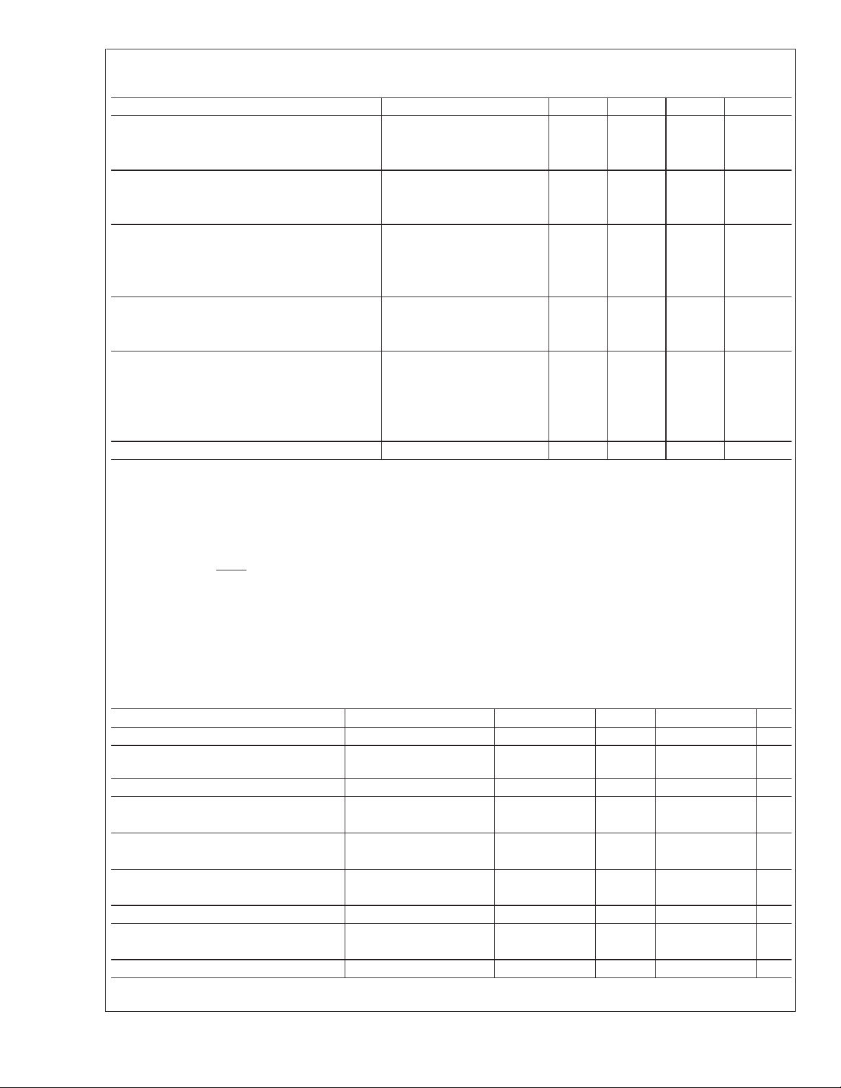
AC Electrical Characteristics 68xEK:
−55˚C ≤ TA≤ +125˚C unless otherwise specified
COP888EK
Instruction Cycle Time (t
Crystal, Resonator 4.5V ≤ V
R/C Oscillator 4.5V ≤ V
Inputs
t
SETUP
t
HOLD
Output Propagation Delay (Note 23) R
t
PD1,tPD0
SO, SK 4.5V ≤ VCC≤ 5.5V 0.7 µs
All Others 4.5V ≤ V
MICROWIRE Setup Time (t
MICROWIRE Hold Time (t
MICROWIRE Output Propagation Delay (t
Input Pulse Width (Note 24)
Interrupt Input High Time 1.0 t
Interrupt Input Low Time 1.0 t
Timer 1, 2, 3 Input High Time 1.0 t
Timer 1, 2, 3 Input Low Time 1.0 t
Reset Pulse Width 1.0 µs
Note 18: t
Note 19: Maximum rate of voltage change must be
Note 20: Supply and IDLE currents are measured with CKI driven with a square wave Oscillator, CKO driven 180˚ out of phase with CKI, inputs connected to V
and outputs driven low but not connected to a load.
Note 21: The HALTmode will stop CKI from oscillating in the RC and the Crystal configurations. Measurement of I
sinking current; with L, C, G0, and G2–G5 programmed as low outputs and not driving a load; all outputs programmed low and not driving a load; all inputs tied to
V
CC
in crystal clock mode.
Note 22: Pins G6 and RESET are designed with a high voltage input network. These pins allow input voltages
biased at voltages>VCC(the pins do not have source current when biased at a voltage below VCC). The effective resistance to VCCis 750Ω (typical). These two
pins will not latch up. The voltage at the pins must be limited to
cludes ESD transients.
Note 23: The output propagation delay is referenced to the end of the instruction cycle where the output change occurs.
Note 24: Parameter characterized but not tested.
=
c
; clock monitor and comparator disabled. Parameter refers to HALT mode entered via setting bit 7 of the G Port data register. Part will pull up CKI during HALT
Parameter Conditions Min Typ Max Units
)
c
≤ 5.5V 1.0 DC µs
CC
<
5.5V 3.0 DC µs
CC
4.5V ≤ VCC≤ 5.5V 200 ns
4.5V ≤ VCC≤ 5.5V 60 ns
UWS
UWH
Instruction Cycle Time
=
2.2k, C
L
) (Note 23) VCC≥ 4.5V 20 ns
) (Note 23) VCC≥ 4.5V 56 ns
)VCC≥ 4.5V 220 ns
UPD
<
0.5 V/ms.
<
14V.WARNING: Voltages in excess of 14V will cause damage to the pins. This warning ex-
=
100 pF
L
≤ 5.5V 1.0 µs
CC
HALTis done with device neither sourcing nor
DD
>
VCCand the pins will have sink current to VCCwhen
c
c
c
c
CC
Analog Function Block AC and DC Characteristics
=
V
5.0V, −40˚C ≤ T
CC
Parameter Conditions Min Typ Max Units
Input Offset Voltage 0.4V
Input Common Mode Voltage Range
(Note 26)
V
/2 Reference 4.0V<V
CC
DC Supply Current for
Comparator (when enabled)
DC Supply Current for
V
/2 Reference (when enabled)
CC
DC Supply Current for
Constant Current Source (when enabled)
Constant Current Source 4.0V
Current Source Variation over 4.0V
Common Mode Range Temp=Constant
Current Source Enable Time 1.5 2 µs
www.national.com 10
≤ +85˚C
A
<
<
V
VCC− 1.5V
IN
0.4 V
<
6.0V 0.5 VCC− 0.04 0.5 V
CC
=
V
6.0V
CC
=
V
6.0V
CC
=
V
6.0V
CC
<
<
V
6.0V 10 20 40 µA
CC
<
<
V
6.0V
CC
±
10
CC
±
25 mV
− 1.5 V
CC
0.5 VCC+ 0.04 V
250 µA
50 80 µA
200 µA
±
2µA
Analog Function Block AC and DC Characteristics (Continued)
=
V
5.0V, −40˚C ≤ T
CC
Parameter Conditions Min Typ Max Units
Comparator Response Time 100 mV Overdrive, 1 µs
Note 25: While performance characteristics are given at V
/2 reference and the constant current source is not guaranteed beyond the specified limits.
V
CC
Note 26: The device is capable of operating over a common mode voltage range of 0 to V
and 0.4V.
≤ +85˚C
A
100 pF Load
=
5.0V, the analog function block will operate over the entire 2.5V–6.0V V
CC
− 1.5V, however increased offset voltage will be observed between 0V
CC
DS012094-18
FIGURE 3. MICROWIRE/PLUS Timing
range. Accuracy of the
CC
COP888EK
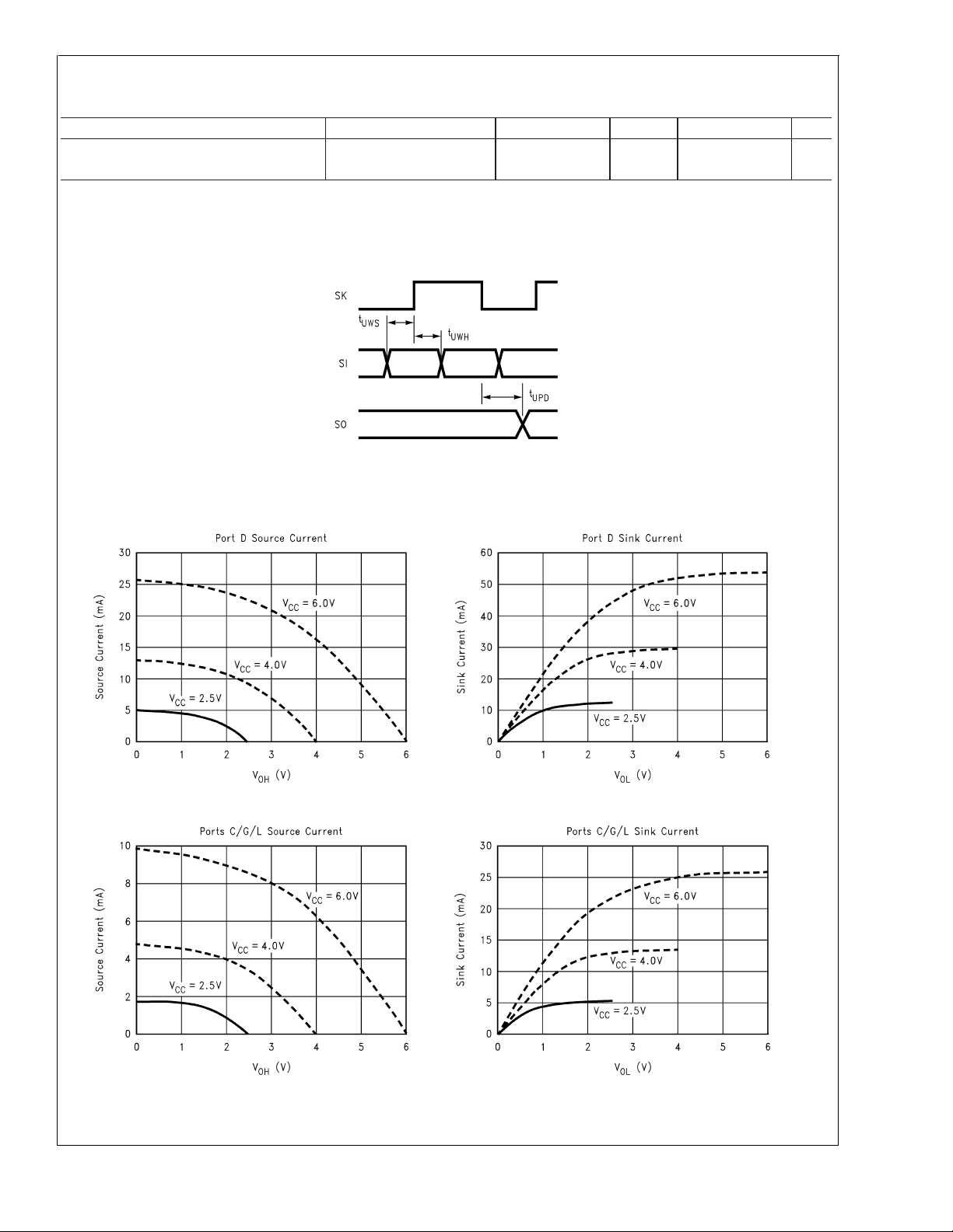
Typical Performance Characteristics (−55˚C ≤ T
DS012094-19 DS012094-20
A
=
+125˚C)
DS012094-21 DS012094-22
www.national.com11
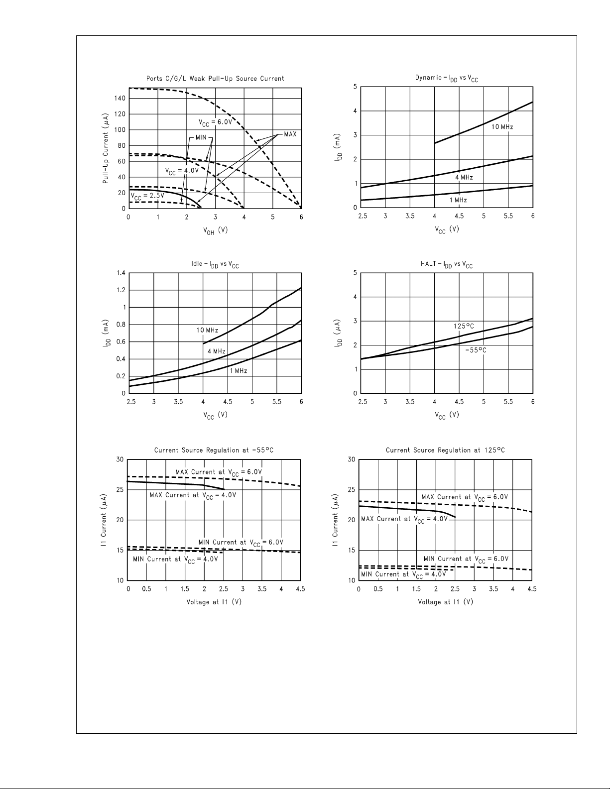
Typical Performance Characteristics (−55˚C ≤ T
COP888EK
=
+125˚C) (Continued)
A
DS012094-23
DS012094-25 DS012094-26
DS012094-24
DS012094-27 DS012094-28
www.national.com 12
COP888EK
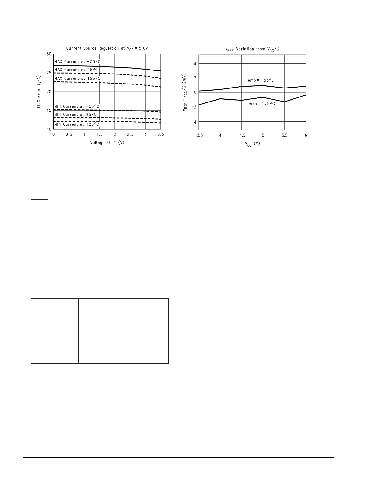
Typical Performance Characteristics (−55˚C ≤ T
DS012094-29
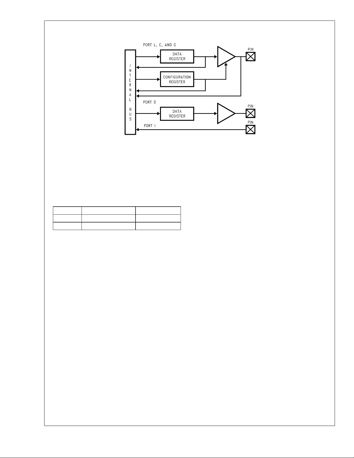
Pin Descriptions
VCCand GND are the power supply pins. All VCCand GND
pins must be connected.
CKI is the clock input. This can come from an R/C generated
oscillator, or a crystal oscillator (in conjunction with CKO).
See Oscillator Description section.
RESET is the master reset input. See Reset Description section.
The device contains three bidirectional 8-bit I/O ports (C, G
and L), where each individual bit may be independently configured as an input (Schmitt Trigger inputs on ports L and G),
output or TRI-STATE under program control. Three data
memory address locations are allocated for each of these
I/O ports. Each I/O port has two associated 8-bit memory
mapped registers, the CONFIGURATION register and the
output DATA register.A memory mapped address is also reserved for the input pins of each I/O port. (See the memory
map for the various addresses associated with the I/O ports.)
Figure 4
CONFIGURATION registers allow for each port bit to be individually configured under software control as shown below:
shows the I/O port configurations. The DATA and
CONFIGURA-
TION
Register Register
0 0 Hi-Z Input
0 1 Input with Weak Pull-Up
1 0 Push-Pull Zero Output
1 1 Push-Pull One Output
DATA
Port Set-Up
(TRI-STATE Output)
The Port L has the following alternate features:
L7 MIWU or T3B
L6 MIWU or T3A
L5 MIWU or T2B
L4 MIWU or T2A
L3 MIWU
L2 MIWU
L1 MIWU
L0 MIWU
Port G is an 8-bit port with 5 I/O pins (G0, G2–G5), an input
pin (G6), and a dedicated output pin (G7). Pins G0 and
G2–G6 all have Schmitt Triggers on their inputs. Pin G1
serves as the dedicated WDOUT WATCHDOG output, while
pin G7 is either input or output depending on the oscillator
mask option selected. With the crystal oscillator option selected, G7 serves as the dedicated output pin for the CKO
clock output. With the single-pin R/C oscillator mask option
selected, G7 serves as a general purpose input pin but is
also used to bring the device out of HALTmode with a low to
high transition on G7. There are two registers associated
with the G Port, a data register and a configuration register.
Therefore, each of the 5 I/O bits (G0, G2–G5) can be individually configured under software control.
Since G6 is an input only pin and G7 is the dedicated CKO
clock output pin (crystal clock option) or general purpose input (R/C clock option), the associated bits in the data and
configuration registers for G6 and G7 are used for special
purpose functions as outlined on the next page. Reading the
G6 and G7 data bits will return zeros.
=
+125˚C) (Continued)
A
DS012094-30
PORT L is an 8-bit I/O port. All L-pins have Schmitt triggers
on the inputs.
The Port L supports Multi-Input Wake Up on all eight pins. L4
and L5 are used for the timer input functions T2A and T2B.
L6 and L7 are used for the timer input functions T3A and
T3B.
www.national.com13
Pin Descriptions (Continued)
COP888EK
FIGURE 4. I/O Port Configurations
Note that the chip will be placed in the HALT mode by writing
a “1” to bit 7 of the Port G Data Register. Similarly the chip
will be placed in the IDLE mode by writing a “1” to bit 6 of the
Port G Data Register.
Writing a “1” to bit 6 of the Port G Configuration Register enables the MICROWIRE/PLUS to operate with the alternate
phase of the SK clock. The G7 configuration bit, if set high,
enables the clock start up delay after HALT when the R/C
clock configuration is used.
Config Reg. Data Reg.
G7 CLKDLY HALT
G6 Alternate SK IDLE
Port G has the following alternate features:
G6 SI (MICROWIRE Serial Data Input)
G5 SK (MICROWIRE Serial Clock)
G4 SO (MICROWIRE Serial Data Output)
G3 T1A (Timer T1 I/O)
G2 T1B (Timer T1 Capture Input)
G0 INTR (External Interrupt Input)
Port G has the following dedicated functions:
G7 CKO Oscillator dedicated output or general purpose
input
G1 WDOUT WATCHDOG and/or Clock Monitor dedi-
cated output
Port C is an 8-bit I/O port. The 40-pin device does not have
a full complement of Port C pins. The unavailable pins are
not terminated. A read operation for these unterminated pins
will return unpredicatable values.
PORTI is an eight-bit Hi-Z input port. The 28-pin device does
not have a full complement of Port I pins. The unavailable
pins are not terminated i.e., they are floating. A read operation for these unterminated pins will return unpredictable values. The user must ensure that the software takes this into
account by either masking or restricting the accesses to bit
operations. The unterminated Port I pins will draw power
only when addressed.
Port I is an eight-bit Hi-Z input port.
Port I0–I7 are used for the analog function block.
The Port I has the following alternate features:
I7 COMPOUT (Comparator Output)
I6 COMPIN5+ (Comparator Positive Input 5)
DS012094-5
I5 COMPIN4+ (Comparator Positive Input 4)
I4 COMPIN3+ (Comparator Positive Input 3)
I3 COMPOUT/COMPIN2+ (Comparator Output/
Comparator Positive Input 2))
I2 COMPIN0+ (Comparator Positive Input 0)
I1 COMPIN− (Comparator Negative Input/Current
Source Out)
I0 COMPIN1+ (Comparator Positive Input 1)
Port D is an 8-bit output port that is preset high when RESET
goes low. The user can tie two or more D port outputs (except D2) together in order to get a higher drive.
Note: Care must be exercised with the D2 pin operation. At RESET, the ex-
ternal loads on this pin must ensure that the output voltages stay
above 0.8 V
keep the external loading on D2 to
to prevent the chip from entering special modes. Also
CC
<
1000 pF.
Functional Description
The architecture of the device is modified Harvard architecture. With the Harvard architecture, the control store program memory (ROM) is separated from the data store
memory (RAM). Both ROM and RAM have their own separate addressing space with separate address buses. The architecture, though based on Harvard architecture, permits
transfer of data from ROM to RAM.
CPU REGISTERS
The CPU can do an 8-bit addition, subtraction, logical or shift
operation in one instruction (t
There are six CPU registers:
A is the 8-bit Accumulator Register
PC is the 15-bit Program Counter Register
PU is the upper 7 bits of the program counter (PC)
PL is the lower 8 bits of the program counter (PC)
B is an 8-bit RAM address pointer, which can be optionally
post auto incremented or decremented.
X is an 8-bit alternate RAM address pointer, which can be
optionally post auto incremented or decremented.
SP is the 8-bit stack pointer, which points to the subroutine/
interrupt stack (in RAM). The SP is initialized to RAM address 06F with reset.
) cycle time.
c
www.national.com 14
 Loading...