

查询COP980C供应商
Connection Diagrams
Dual-In-Line Package
DS010802-23
Top View
Order Number COP882C-XXX/N, COP982C-XXX/N,
COP882C-XXX/WM, COP982C-XXX/WM,
COP982C-XXX/N or COP982CH-XXX/WM
Dual-In-Line Package (N)
and 28 Wide SO (WM)
DS010802-5
Top View
Order Number COP881C-XXX/N, COP981C-XXX/N,
COP881C-XXX/WM, COP981C-XXX/WM,
COP981CH-XXX/N or COP981CH-XXX/WM
Dual-In-Line Package
DS010802-4
Top View
Order Number COP680C-XXX/N, COP880C-XXX/N,
COP980C-XXX/N or COP980CH-XXX/N
Plastic Chip Carrier
DS010802-3
Top View
Order Number COP680C-XXX/V, COP880C-XXX/V,
COP980C-XXX/V or COP980CH-XXX/V
FIGURE 2. Connection Diagrams
COP880C
www.national.com3
COP980C/COP981C/COP982C
Absolute Maximum Ratings
(Note 1)
If Military/Aerospace specified devices are required,
please contact the National Semiconductor Sales Office/
Distributors for availability and specifications.
Supply Voltage (V
CC
)7V
Voltage at any Pin −0.3V to V
CC
+ 0.3V
Total Current into V
CC
Pin (Source) 50 mA
Total Current out of GND Pin (Sink) 60 mA
Storage Temperature Range −65˚C to +140˚C
Note 1: Absolute maximum ratings indicate limits beyond which damage to
the device may occur. DC and AC electrical specifications are not ensured
when operating the device at absolute maximum ratings.
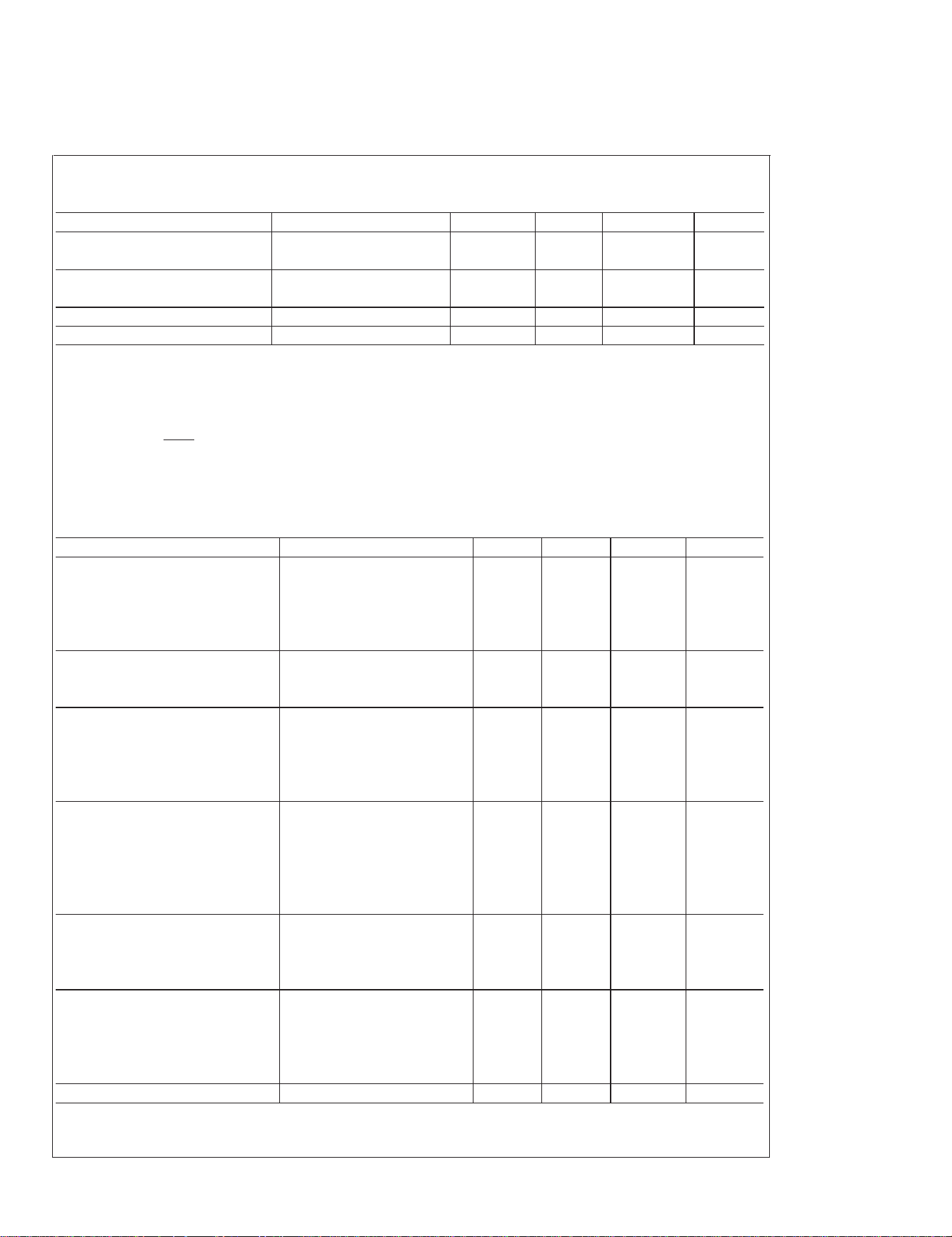
DC Electrical Characteristics
COP98xC; 0˚C ≤ TA≤ +70˚C unless otherwise specified
Parameter Condition Min Typ Max Units
Operating Voltage
98XC 2.3 4.0 V
98XCH 4.0 6.0 V
Power Supply Ripple (Note 2) Peak to Peak 0.1 V
CC
V
Supply Current
CKI = 10 MHz V
CC
= 6V, tc = 1 µs 6.0 mA
CKI = 4 MHz V
CC
= 6V, tc = 2.5 µs 4.4 mA
CKI = 4 MHz V
CC
= 4.0V, tc = 2.5 µs 2.2 mA
CKI = 1 MHz V
CC
= 4.0V, tc = 10 µs 1.4 mA
(Note 3)
HALT Current V
CC
= 6V, CKI = 0 MHz
<
0.7 8 µA
(Note 4) V
CC
= 4.0V, CKI = 0 MHz
<
0.4 5 µA
Input Levels
RESET, CKI
Logic High 0.9 V
CC
V
Logic Low 0.1 V
CC
V
All Other Inputs
Logic High 0.7 V
CC
V
Logic Low 0.2 V
CC
V
Hi-Z Input Leakage V
CC
= 6.0V −1.0 +1.0 µA
Input Pullup Current V
CC
= 6.0V, VIN= 0V −40 −250 µA
G Port Input Hysteresis 0.35 V
CC
V
Output Current Levels
D Outputs
Source V
CC
= 4.5V, VOH= 3.8V −0.4 mA
V
CC
= 2.3V, VOH= 1.6V −0.2 mA
Sink V
CC
= 4.5V, VOL= 1.0V 10 mA
V
CC
= 2.3V, VOL= 0.4V 2 mA
All Others
Source (Weak Pull-Up) V
CC
= 4.5V, VOH= 3.2V −10 −110 µA
V
CC
= 2.3V, VOH= 1.6V −2.5 −33 µA
Source (Push-Pull Mode) V
CC
= 4.5V, VOH= 3.8V −0.4 mA
V
CC
= 2.3V, VOH= 1.6V −0.2
Sink (Push-Pull Mode) V
CC
= 4.5V, VOL= 0.4V 1.6 mA
V
CC
= 2.3V, VOL= 0.4V 0.7
TRI-STATE Leakage V
CC
= 6.0V −1.0 +1.0 µA
Allowable Sink/Source
Current Per Pin
D Outputs (Sink) 15 mA
All Others 3mA
COP880C
www.national.com 4
DC Electrical Characteristics (Continued)
COP98xC; 0˚C ≤ TA≤ +70˚C unless otherwise specified
Parameter Condition Min Typ Max Units
Maximum Input Current (Note 5)
Without Latchup (Room Temp) Room Temp
±
100 mA
RAM Retention Voltage, Vr 500 ns Rise and
(Note 6) Fall Time (Min) 2.0 V
Input Capacitance 7pF
Load Capacitance on D2 1000 pF
COP980C/COP981C/COP982C
Note 2: Rate of voltage change must be less than 0.5V/ms.
Note 3: Supply current is measured after running 2000 cycles with a square wave CKI input, CKO open, inputs at rails and outputs open.
Note 4: The HALT mode willstop CKI from oscillating in the RC and the Crystal configurations. Test conditions: All inputs tied to V
CC
, L, C and G ports TRI-STATE
and tied to ground, all outputs low and tied to ground.
Note 5: Pins G6 and RESET are designed with a high voltage input network for factory testing. These pins allow input voltages greater than V
CC
and the pins will
have sink current to VCCwhen biased at voltages greater than VCC(the pins do not have source current when biased at a voltage below VCC). The effective
resistance to V
CC
is 750Ω (typ). These two pins will not latch up. The voltage at the pins must be limited to less than 14V.
Note 6: To maintain RAM integrity, the voltage must not be dropped or raised instantaneously.
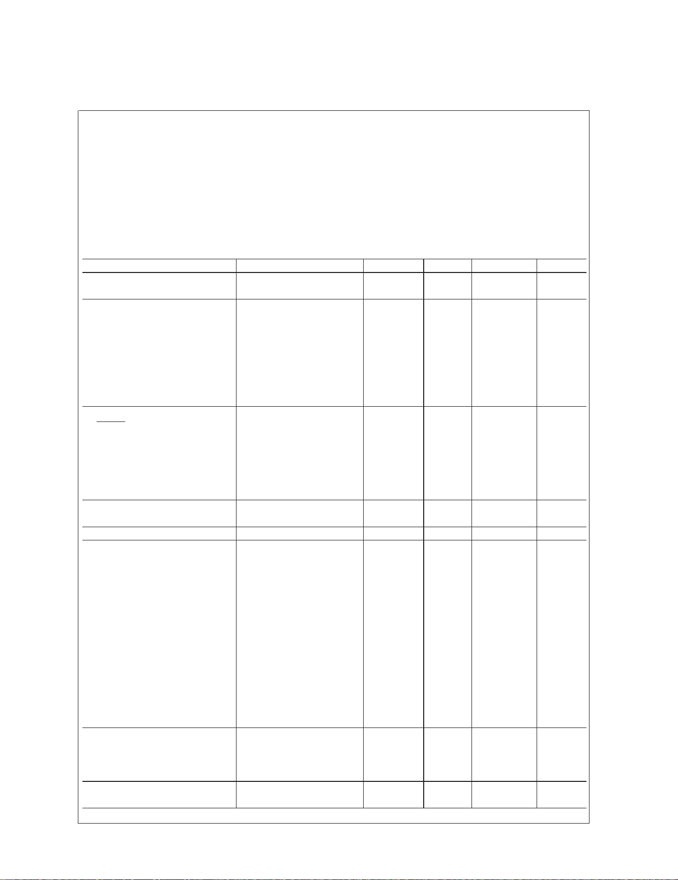
AC Electrical Characteristics
0˚C ≤ TA≤ +70˚C unless otherwise specified
Parameter Condition Min Typ Max Units
Instruction Cycle Time (tc)
Crystal/Resonator or External V
CC
≥ 4.0V 1 DC µs
(Div-by 10) 2.3V ≤ V
CC
≤ 4.0V 2.5 DC µs
R/C Oscillator Mode V
CC
≥ 4.0V 3 DC µs
(Div-by 10) 2.3V ≤ V
CC
≤ 4.0V 7.5 DC µs
CKI Clock Duty Cycle (Note 7) fr = Max 40 60 %
Rise Time (Note 7) fr = 10 MHz Ext Clock 12 ns
Fall Time (Note 7) fr = 10 MHz Ext Clock 8 ns
Inputs
t
SETUP
VCC≥ 4.0V 200 ns
2.3V ≤ V
CC
≤ 4.0V 500 ns
t
HOLD
VCC≥ 4.0V 60 ns
2.3V ≤ V
CC
≤ 4.0V 150 ns
Output Propagation Delay C
L
= 100 pF, RL= 2.2 kΩ
t
PD1,tPD0
SO, SK VCC≥ 4.0V 0.7 µs
2.3V ≤ V
CC
≤ 4.0V 1.75 µs
All Others V
CC
≥ 4.0V 1 µs
2.3V ≤ V
CC
≤ 4.0V 2.5 µs
MICROWIRE
™
Setup Time (t
UWS)
20 ns
MICROWIRE Hold Time (t
UWH)
56 ns
MICROWIRE Output
Propagation Delay (t
UPD
) 220 ns
Input Pulse Width
Interrupt Input High Time t
C
Interrupt Input Low Time t
C
Timer Input High Time t
C
Timer Input Low Time t
C
Reset Pulse Width 1.0 µs
Note 7: Parameter characterized but not production tested.
COP880C
www.national.com5
COP880C/COP881C/COP882C
Absolute Maximum Ratings
(Note 8)
If Military/Aerospace specified devices are required,
please contact the National Semiconductor Sales Office/
Distributors for availability and specifications.
Supply Voltage (V
CC
)7V
Voltage at any Pin −0.3V to V
CC
+ 0.3V
Total Current into V
CC
Pin (Source) 50 mA
Total Current out of GND Pin (Sink) 60 mA
Storage Temperature Range −65˚C to +140˚C
Note 8: Absolute maximum ratings indicate limits beyond which damage to
the device may occur. DC and AC electrical specifications are not ensured
when operating the device at absolute maximum ratings.
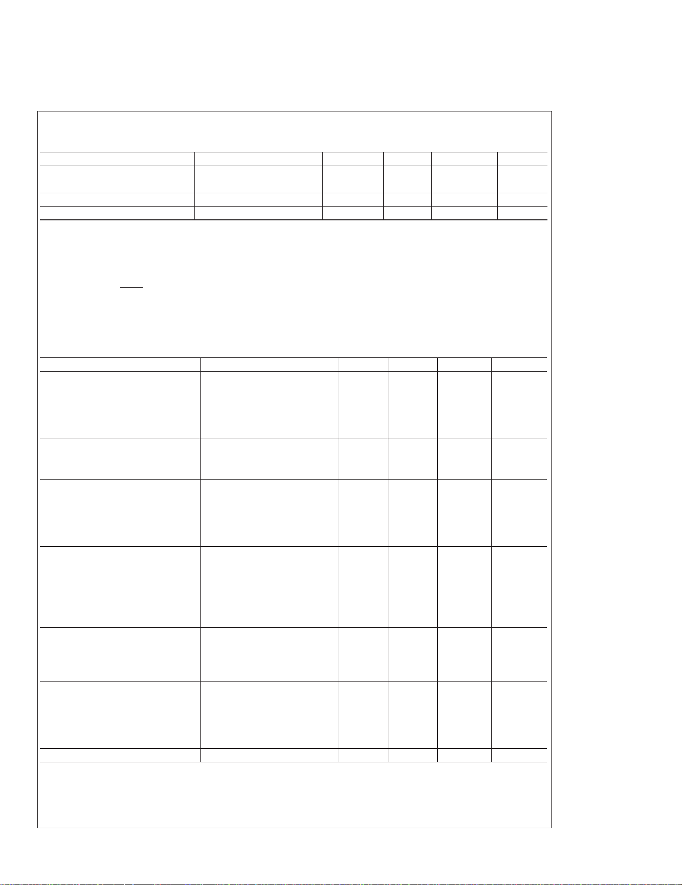
DC Electrical Characteristics
COP88xC; −40˚C ≤ TA≤ +85˚C unless otherwise specified
Parameter Condition Min Typ Max Units
Operating Voltage 2.5 6.0 V
Power Supply Ripple (Note 9) Peak to Peak 0.1 V
CC
V
Supply Current
CKI = 10 MHz V
CC
= 6V, tc = 1 µs 6.0 mA
CKI = 4 MHz V
CC
= 6V, tc = 2.5 µs 4.4 mA
CKI = 4 MHz V
CC
= 4.0V, tc = 2.5 µs 2.2 mA
CKI = 1 MHz V
CC
= 4.0V, tc = 10 µs 1.4 mA
(Note 10)
HALT Current V
CC
= 6V, CKI = 0 MHz
<
110 µA
(Note 11) V
CC
= 3.5V, CKI = 0 MHz
<
0.5 6 µA
Input Levels
RESET, CKI
Logic High 0.9 V
CC
V
Logic Low 0.1 V
CC
V
All Other Inputs
Logic High 0.7 V
CC
V
Logic Low 0.2 V
CC
V
Hi-Z Input Leakage V
CC
= 6.0V −2 +2 µA
Input Pullup Current V
CC
= 6.0V, VIN= 0V −40 −250 µA
G Port Input Hysteresis 0.35 V
CC
V
Output Current Levels
D Outputs
Source V
CC
= 4.5V, VOH= 3.8V −0.4 mA
V
CC
= 2.5V, VOH= 1.8V −0.2 mA
Sink V
CC
= 4.5V, VOL= 1.0V 10 mA
V
CC
= 2.5V, VOL= 0.4V 2 mA
All Others
Source (Weak Pull-Up) V
CC
= 4.5V, VOH= 3.2V −10 −110 µA
V
CC
= 2.5V, VOH= 1.8V −2.5 −33 µA
Source (Push-Pull Mode) V
CC
= 4.5V, VOH= 3.8V −0.4 mA
V
CC
= 2.5V, VOH= 1.8V −0.2
Sink (Push-Pull Mode) V
CC
= 4.5V, VOL= 0.4V 1.6 mA
V
CC
= 2.5V, VOL= 0.4V 0.7
TRI-STATE Leakage V
CC
= 6.0V −2.0 +2.0 µA
Allowable Sink/Source
Current Per Pin
D Outputs (Sink) 15 mA
All Others 3mA
Maximum Input Current (Note 12)
Without Latchup (Room Temp) Room Temp
±
100 mA
COP880C
www.national.com 6
DC Electrical Characteristics (Continued)
COP88xC; −40˚C ≤ TA≤ +85˚C unless otherwise specified
Parameter Condition Min Typ Max Units
RAM Retention Voltage, Vr 500 ns Rise and
(Note 13) Fall Time (Min) 2.0 V
Input Capacitance 7pF
Load Capacitance on D2 1000 pF
COP880C/COP881C/COP882C
Note 9: Rate of voltage change must be less than 0.5V/ms.
Note 10: Supply current is measured after running 2000 cycles with a square wave CKI input, CKO open, inputs at rails and outputs open.
Note 11: The HALT mode will stop CKI from oscillating in the RC and the Crystal configurations. Testconditions:All inputs tied to V
CC
, L, C and G ports TRI-STATE
and tied to ground, all outputs low and tied to ground.
Note 12: Pins G6 and RESET are designed with a high voltage input network for factory testing. These pins allow input voltages greater than V
CC
and the pins will
have sink current to VCCwhen biased at voltages greater than VCC(the pins do not have source current when biased at a voltage below VCC). The effective
resistance to V
CC
is 750Ω (typ). These two pins will not latch up. The voltage at the pins must be limited to less than 14V.
Note 13: To maintain RAM integrity, the voltage must not be dropped or raised instantaneously.
AC Electrical Characteristics
−40˚C ≤ TA≤ +85˚C unless otherwise specified
Parameter Condition Min Typ Max Units
Instruction Cycle Time (tc)
Crystal/Resonator or External V
CC
≥ 4.5V 1 DC µs
(Div-by 10) 2.5V ≤ V
CC
<
4.5V 2.5 DC µs
R/C Oscillator Mode V
CC
≥ 4.5V 3 DC µs
(Div-by 10) 2.5V ≤ V
CC
<
4.5V 7.5 DC µs
CKI Clock Duty Cycle (Note 14) fr = Max 40 60 %
Rise Time (Note 14) fr = 10 MHz Ext Clock 12 ns
Fall Time (Note 14) fr = 10 MHz Ext Clock 8 ns
Inputs
t
SETUP
VCC≥ 4.5V 200 ns
2.5V ≤ V
CC
<
4.5V 500 ns
t
HOLD
VCC≥ 4.5V 60 ns
2.5V ≤ V
CC
<
4.5V 150 ns
Output Propagation Delay C
L
= 100 pF, RL= 2.2 kΩ
t
PD1,tPD0
SO, SK VCC≥ 4.5V 0.7 µs
2.5V ≤ V
CC
<
4.5V 1.75 µs
All Others V
CC
≥ 4.5V 1 µs
2.5V ≤ V
CC
<
4.5V 2.5 µs
MICROWIRE Setup Time (t
UWS)
20 ns
MICROWIRE Hold Time (t
UWH)
56 ns
MICROWIRE Output
Propagation Delay (t
UPD
) 220 ns
Input Pulse Width
Interrupt Input High Time t
C
Interrupt Input Low Time t
C
Timer Input High Time t
C
Timer Input Low Time t
C
Reset Pulse Width 1.0 µs
Note 14: Parameter characterized but not production tested.
COP880C
www.national.com7
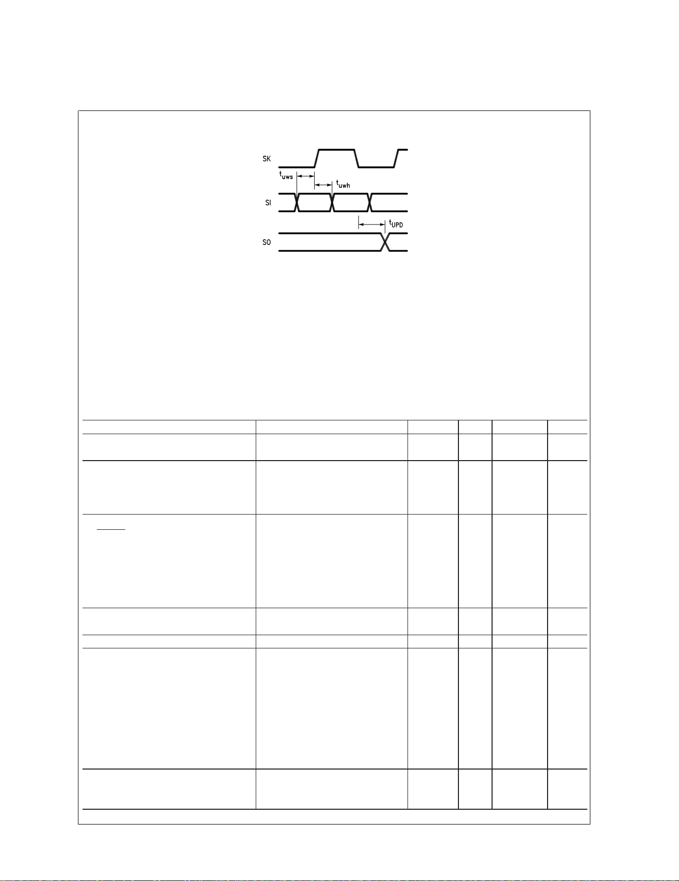
Timing Diagram
COP680C/COP681C/COP682C
Absolute Maximum Ratings
(Note 16)
If Military/Aerospace specified devices are required,
please contact the National Semiconductor Sales Office/
Distributors for availability and specifications.
Supply Voltage (V
CC
)6V
Voltage at Any Pin −0.3V to V
CC
+ 0.3V
Total Current into V
CC
Pin (Source) 40 mA
Total Current Out of GND Pin (Sink) 48 mA
Storage Temperature Range −65˚C to +140˚C
Note 15:
Absolute maximum ratings indicate limits beyond which damage to
the device may occur. DC and AC electrical specifications are not ensured
when operating the device at absolute maximum ratings.
DC Electrical Characteristics
COP68xC: −55˚C ≤ TA≤ +125˚C unless otherwise specified
Parameter Condition Min Typ Max Units
Operating Voltage 4.5 5.5 V
Power Supply Ripple (Note 17) Peak to Peak 0.1 V
CC
V
Supply Current (Note 18)
CKI = 10 MHz V
CC
= 5.5V, tc = 1 µs 8.0 mA
CKI = 4 MHz V
CC
= 5.5V, tc = 2.5 µs 4.4 mA
HALT Current (Note 19) V
CC
= 5.5V, CKI = 0 MHz
<
10 30 µA
Input Levels
RESET, CKI
Logic High 0.9 V
CC
V
Logic Low 0.1 V
CC
V
All Other Inputs
Logic High 0.7 V
CC
V
Logic Low 0.2 V
CC
V
Hi-Z Input Leakage V
CC
= 5.5V −5 +5 µA
Input Pullup Current V
CC
= 5.5V, VIN= 0V −35 −300 µA
G Port Input Hysteresis 0.35 V
CC
V
Output Current Levels
D Outputs
Source V
CC
= 4.5V, VOH= 3.8V −0.35 mA
Sink V
CC
= 4.5V, VOL= 1.0V 9 mA
All Others
Source (Weak Pull-Up) V
CC
= 4.5V, VOH= 3.2V −9 −120 µA
Source (Push-Pull Mode) V
CC
= 4.5V, VOH= 3.2V −0.35 mA
Sink (Push-Pull Mode) V
CC
= 4.5V, VOL= 0.4V 1.4 mA
TRI-STATE Leakage V
CC
= 5.5V −5.0 +5.0 µA
Allowable Sink/Source Current per Pin
D Outputs (Sink) 12 mA
All Others 2.5 mA
DS010802-2
FIGURE 3. MICROWIRE/PLUS Timing
COP880C
www.national.com 8
DC Electrical Characteristics (Continued)
COP68xC: −55˚C ≤ TA≤ +125˚C unless otherwise specified
Parameter Condition Min Typ Max Units
Maximum Input Current (Room Temp)
without Latchup (Note 20) Room Temp
±
100 mA
RAM Retention Voltage, Vr (Note 21) 500 ns Rise and Fall Time (Min) 2.5 V
Input Capacitance 7pF
Load Capacitance on D2 1000 pF
Note 16:
Absolute maximum ratings indicate limits beyond which damage to the device may occur. DC and AC electrical specifications are not ensured when
operating the device at absolute maximum ratings.
Note 17: Rate of voltage change must be less than 0.5V/ms.
Note 18: Supply current is measured after running 2000 cycles with a square wave CKI input, CKO open, inputs at rails and outputs open.
Note 19: The HALT mode will stop CKI from oscillating in the RC and the Crystal configurations. Test conditions: All inputs tied to V
CC
, L and G ports TRI-STATE
and tied to ground, all outputs low and tied to ground.
Note 20: Pins G6 and RESET are designed with a high voltage input network for factory testing. These pins allow input voltages greater than V
CC
and the pins will
have sink current to VCCwhen biased at voltages greater than VCC(the pins do not have source current when biased at a voltage below VCC). The effective
resistance to V
CC
is 750Ω (typical). These two pins will not latch up. The voltage at the pins must be limited to less than 14V.
Note 21: To maintain RAM integrity, the voltage must not be dropped or raised instantaneously.
COP680C/COP681C/COP682C
AC Electrical Characteristics
−55˚C ≤ TA≤ +125˚C unless otherwise specified
Parameter Condition Min Typ Max Units
Instruction Cycle Time (tc)
Ext. or Crystal/Resonant V
CC
≥ 4.5V 1 DC µs
(Div-by 10)
CKI Clock Duty Cycle fr = Max 40 60 %
(Note 22)
Rise Time (Note 22) fr = 10 MHz Ext Clock 12 ns
Fall Time (Note 22) fr = 10 MHz Ext Clock 8 ns
MICROWIRE Setup Time (t
UWS
)20ns
MICROWIRE Hold Time (t
UWH
)56ns
MICROWIRE Output Valid 220 ns
Time (t
UPD
)
Input Pulse Width
Interrupt Input High Time t
C
Interrupt Input Low Time t
C
Timer Input High Time t
C
Timer Input Low Time t
C
Reset Pulse Width 1 µs
Note 22: Parameter characterized but not production tested.
COP880C
www.national.com9
Typical Performance Characteristics (−40˚C ≤ T
A
≤ +85˚C)
Hall—I
DD
DS010802-16
Dynamic—IDD(Crystal Clock Option)
DS010802-17
Port L/C/G Weak Pull-Up
DS010802-18
Port L/C/G Push-Pull Source Current
DS010802-19
Port L/C/G Push-Pull Sink Current
DS010802-20
Port D Source Current
DS010802-21
COP880C
www.national.com 10
Typical Performance Characteristics (−40˚C ≤ T
A
≤ +85˚C) (Continued)
Pin Descriptions
VCCand GND are the power supply pins.
CKI is the clock input. This can come from an external
source, a R/C generated oscillator or a crystal (in conjunction with CKO). See Oscillator description.
RESET is the master reset input. See Reset description.
PORTI is an 8-bit Hi-Z input port. The 28-pin device does not
have a full complement of Port I pins. The unavailable pins
are not terminated i.e., they are floating. A read operation for
these unterminated pins will return unpredictable values.
The user must ensure that the software takes this into account by either masking or restricting the accesses to bit
operations. The unterminated Port I pins will draw power
only when addressed.
PORT L is an 8-bit I/O port.
PORT C is a 4-bit I/O port.
Three memory locations are allocated for the L, G and C
ports, one each for data register, configuration register and
the input pins. Reading bits 4–7 of the C-Configuration register, data register, and input pins returns undefined data.
There are two registers associated with the L and C ports: a
data register and a configuration register. Therefore, each L
and C I/O bit can be individually configured under software
control as shown below:
Con-
fig.
Data Ports L and C Setup
0 0 Hi-Z Input (TRI-STATE Output)
0 1 Input with Pull-Up (Weak One Output)
1 0 Push-Pull Zero Output
1 1 Push-Pull One Output
On the 28-pin part, it is recommended that all bits of Port C
be configured as outputs.
PORT G is an 8-bit port with 6 I/O pins (G0–G5)and 2 input
pins (G6, G7). All eight G-pins have Schmitt Triggers on the
inputs.
There are two registers associated with the G port: a data
register and a configuration register. Therefore, each G port
bit can be individually configured under software control as
shown below:
Con-
fig.
Data Port G Setup
0 0 Hi-Z Input (TRI-STATE Output)
0 1 Input with Pull-Up (Weak One Output)
1 0 Push-Pull Zero Output
1 1 Push-Pull One Output
Since G6 and G7 are input only pins, any attempt by the user
to configure them as outputs by writing a one to the configuration register will be disregarded. Reading the G6 and G7
configuration bits will return zeros. The device will be placed
in the HALT mode by writing to the G7 bit in the G-port data
register.
Six pins of Port G have alternate features:
G0 INTR (an external interrupt)
G3 TIO (timer/counter input/output)
G4 SO (MICROWIRE serial data output)
G5 SK (MICROWIRE clock I/O)
G6 SI (MICROWIRE serial data input)
G7 CKO crystal oscillator output (selected by mask option)
or HALT restart input (general purpose input)
Pins G1 and G2 currently do not have any alternate functions.
PORT D is an 8-bit output port that is preset high when
RESET goes low. Care must be exercised with the D2 pin
operation. At RESET, the external loads on this pin must
ensure that the output voltages stay above 0.9 V
CC
to prevent the chip from entering special modes. Also, keep the
external loading on D2 to less than 1000 pF.
Functional Description
Figure 1
shows the block diagram of the internal architecture. Data paths are illustrated in simplified form to depict
how the various logic elements communicate with each
other in implementing the instruction set of the device.
ALU AND CPU REGISTERS
The ALU can do an 8-bit addition, subtraction, logical or shift
operation in one cycle time.
There are five CPU registers:
A is the 8-bit Accumulator register
PU is the upper 7 bits of the program counter (PC)
PL is the lower 8 bits of the program counter (PC)
Port D Sink Current
DS010802-22
COP880C
www.national.com11

Functional Description (Continued)
B is the 8-bit address register, can be auto incremented or
decremented.
X is the 8-bit alternate address register, can be incremented
or decremented.
SP is the 8-bit stack pointer, points to subroutine stack (in
RAM).
B, X and SP registers are mapped into the on chip RAM. The
B and X registers are used to address the on chip RAM. The
SP register is used to address the stack in RAM during
subroutine calls and returns.
PROGRAM MEMORY
Program memory consists of 4096 bytes of ROM. These
bytes may hold program instructions or constant data. The
program memory is addressed by the 15-bit program
counter (PC). ROM can be indirectly read by the LAID instruction for table lookup.
DATA MEMORY
The data memory address space includes on chip RAM, I/O
and registers. Data memory is addressed directly by the
instruction or indirectly by the B, X and SP registers.
The device has 128 bytes of RAM. Sixteen bytes of RAM are
mapped as “registers” that can be loaded immediately, decremented or tested. Three specific registers: B, X and SP are
mapped into this space, the other bytes are available for
general usage.
The instruction set permits any bit in memory to be set, reset
or tested. All I/O and registers (except the A & PC) are
memory mapped; therefore, I/O bits and register bits can be
directly and individually set, reset and tested. A is not
memory mapped, but bit operations can be still performed on
it.
Note: RAM contents are undefined upon power-up.
RESET
The RESET input when pulled low initializes the microcontroller. Initialization will occur whenever the RESET input is
pulled low. Upon initialization, the ports L, G and C are
placed in the TRI-STATE mode and the Port D is set high.
The PC, PSW and CNTRL registers are cleared. The data
and configuration registers for Ports L, G and C are cleared.
The external RC network shown in
Figure 4
should be used
to ensure that the RESET pin is held low until the power
supply to the chip stabilizes.
OSCILLATOR CIRCUITS
Figure 5
shows the three clock oscillator configurations.
A. CRYSTAL OSCILLATOR
The device can be driven by a crystal clock. The crystal
network is connected between the pins CKI and CKO.
Table 1
shows the component values required for various
standard crystal values.
B. EXTERNAL OSCILLATOR
CKI can be driven by an external clock signal. CKO is
available as a general purpose input and/or HALT restart
control.
C. R/C OSCILLATOR
CKI is configured as a single pin RC controlled Schmitt
trigger oscillator. CKO is available as a general purpose
input and/or HALT restart control.
Table 2
shows the variation in the oscillator frequencies as
functions of the component (R and C) values.
OSCILLATOR MASK OPTIONS
The device can be driven by clock inputs between DC and
10 MHz.
TABLE 1. Crystal Oscillator Configuration, T
A
= 25˚C
R1 R2 C1 C2 CKI Freq Conditions
(kΩ)(MΩ) (pF) (pF) (MHz)
0 1 30 30–36 10 V
CC
=5V
0 1 30 30–36 4 V
CC
= 2.5V
5.6 1 200 100–150 0.455 V
CC
=5V
DS010802-6
RC ≥ 5X Power Supply Rise Time
FIGURE 4. Recommended Reset Circuit
DS010802-7
FIGURE 5. Crystal and R-C Connection Diagrams
COP880C
www.national.com 12

Functional Description (Continued)
TABLE 2. RC Oscillator Configuration, T
A
= 25˚C
R C CKI Freq. Instr. Cycle Conditions
(kΩ) (pF) (MHz) (µs)
3.3 82 2.2 to 2.7 3.7 to 4.6 V
CC
=5V
5.6 100 1.1 to 1.3 7.4 to 9.0 V
CC
=5V
6.8 100 0.9 to 1.1 8.8 to 10.8 V
CC
=5V
Note 23: (R/C Oscillator Configuration): 3k ≤ R ≤ 200k, 50 pF ≤ C ≤ 200 pF.
The device has three mask options for configuring the clock
input. The CKI and CKO pins are automatically configured
upon selecting a particular option.
•
Crystal (CKI/10); CKO for crystal configuration
•
External (CKI/10); CKO available as G7 input
•
R/C (CKI/10); CKO available as G7 input
G7 can be used either as a general purpose input or as a
control input to continue from the HALT mode.
HALT MODE
The device supports a power saving mode of operation:
HALT. The controller is placed in the HALT mode by setting
the G7 data bit, alternatively the user can stop the clock
input. In the HALT mode all internal processor activities
including the clock oscillator are stopped. The fully static
architecture freezes the state of the controller and retains all
information until continuing. In the HALT mode, power requirements are minimal as it draws only leakage currents
and output current. The applied voltage (V
CC
) may be decreased down to Vr (minimum RAM retention voltage) without altering the state of the machine.
There are two ways to exit the HALT mode: via the RESET
or by the CKO pin. A low on the RESET line reinitializes the
microcontroller and starts executing from the address
0000H. A low to high transition on the CKO pin (only if the
external or R/C clock option selected) causes the microcontroller to continue with no reinitialization from the address
following the HALT instruction. This also resets the G7 data
bit.
INTERRUPTS
There are three interrupt sources, as shown below.
A maskable interrupt on external G0 input (positive or nega-
tive edge sensitive under software control)
A maskable interrupt on timer underflow or timer capture
A non-maskable software/error interrupt on opcode zero
INTERRUPT CONTROL
The GIE (global interrupt enable) bit enables the interrupt
function. This is used in conjunction with ENI and ENTI to
select one or both of the interrupt sources. This bit is reset
when interrupt is acknowledged.
ENI and ENTI bits select external and timer interrupt respectively. Thus the user can select either or both sources to
interrupt the microcontroller when GIE is enabled.
IEDG selects the external interrupt edge (0 = rising edge,
1 = falling edge). The user can get an interrupt on both rising
and falling edges by toggling the state of IEDG bit after each
interrupt.
IPND and TPND bits signal which interrupt is pending. After
interrupt is acknowledged, the user can check these two bits
to determine which interrupt is pending. This permits the
interrupts to be prioritized under software. The pending flags
have to be cleared by the user. Setting the GIE bit high
inside the interrupt subroutine allows nested interrupts.
The software interrupt does not reset the GIE bit. This
means that the controller can be interrupted by other interrupt sources while servicing the software interrupt.
INTERRUPT PROCESSING
The interrupt, once acknowledged, pushes the program
counter (PC) onto the stack and the stack pointer (SP) is
decremented twice. The Global Interrupt Enable (GIE) bit is
reset to disable further interrupts. The microcontroller then
vectors to the address 00FFH and resumes execution from
that address. This process takes 7 cycles to complete. At the
end of the interrupt subroutine, any of the following three
instructions return the processor back to the main program:
RET, RETSK or RETI. Either one of the three instructions will
pop the stack into the program counter (PC). The stack
pointer is then incremented twice. The RETI instruction additionally sets the GIE bit to re-enable further interrupts.
Any of the three instructions can be used to return from a
hardware interrupt subroutine. The RETSK instruction
should be used when returning from a software interrupt
subroutine to avoid entering an infinite loop.
Note: There is always the possibility of an interrupt occurring during an
instruction which is attempting to reset the GIE bit or any other interrupt enable bit. If this occurs when a single cycle instruction is being
used to reset the interrupt enable bit, the interrupt enable bit will be
reset but an interrupt may still occur.Thisis because interrupt processing is started at the same time as the interrupt bit is being reset. To
avoid this scenario, the user should always use a two, three or four
cycle instruction to reset interrupt enable bits.
COP880C
www.national.com13
Functional Description (Continued)
DETECTION OF ILLEGAL CONDITIONS
The device contains a hardware mechanism that allows it to
detect illegal conditions which may occur from coding errors,
noise and “brown out” voltage drop situations. Specifically it
detects cases of executing out of undefined ROM area and
unbalanced stack situations.
Reading an undefined ROM location returns 00 (hexadecimal) as its contents. The opcode for a software interrupt is
also “00”. Thus a program accessing undefined ROM will
cause a software interrupt.
Reading an undefined RAM location returns an FF (hexadecimal). The subroutine stack grows down for each subroutine call. By initializing the stack pointer to the top of RAM,
the first unbalanced return instruction will cause the stack
pointer to address undefined RAM. As a result the program
will attempt to execute from FFFF (hexadecimal), which is an
undefined ROM location and will trigger a software interrupt.
MICROWIRE/PLUS
MICROWIRE/PLUS is a serial synchronous bidirectional
communications interface. The MICROWIRE/PLUS capability enables the device to interface with any of National
Semiconductor’s MICROWIRE peripherals (i.e. A/D converters, display drivers, EEPROMS, etc.) and with other microcontrollers which support the MICROWIRE/PLUS interface.
It consists of an 8-bit serial shift register (SIO) with serial
data input (SI), serial data output (SO) and serial shift clock
(SK).
Figure 7
shows the block diagram of the MICROWIRE/
PLUS interface.
The shift clock can be selected from either an internal source
or an external source. Operating the MICROWIRE/PLUS
interface with the internal clock source is called the Master
mode of operation. Similarly, operating the MICROWIRE/
PLUS interface with an external shift clock is called the Slave
mode of operation.
The CNTRL register is used to configure and control the
MICROWIRE/PLUS mode. To use the MICROWIRE/PLUS,
the MSEL bit in the CNTRL register is set to one. The SK
clock rate is selected by the two bits, SL0 and SL1, in the
CNTRL register.
Table 3
details the different clock rates that
may be selected.
TABLE 3.
SL1 SL0 SK Cycle Time
00 2t
C
01 4t
C
1x 8t
C
where,
t
C
is the instruction cycle clock.
MICROWIRE/PLUS OPERATION
Setting the BUSY bit in the PSW register causes the
MICROWIRE/PLUS arrangement to start shifting the data. It
gets reset when eight data bits have been shifted. The user
may reset the BUSY bit by software to allow less than 8 bits
to shift. The devoce may enter the MICROWIRE/PLUS
mode either as a Master or as a Slave.
Figure 8
shows how
two COP880C microcontrollers and several peripherals may
be interconnected using the MICROWIRE/PLUS arrangement.
Master MICROWIRE/PLUS Operation
In the MICROWIRE/PLUS Master mode of operation the
shift clock (SK) is generated internally. The MICROWIRE/
PLUS Master always initiates all data exchanges. (See
Fig-
ure 8
). The MSEL bit in the CNTRL register must be set to
enable the SO and SK functions onto the G Port. The SO
and SK pins must also be selected as outputs by setting
appropriate bits in the Port G configuration register.
Table 4
summarizes the bit settings required for Master mode of
operation.
SLAVE MICROWIRE/PLUS OPERATION
In the MICROWIRE/PLUS Slave mode of operation the SK
clock is generated by an external source. Setting the MSEL
bit in the CNTRL register enables the SO and SK functions
onto the G Port. The SK pin must be selected as an input
and the SO pin is selected as an output pin by appropriately
setting up the Port G configuration register.
Table 4
summarizes the settings required to enter the Slave mode of operation.
The user must set the BUSY flag immediately upon entering
the Slave mode. This will ensure that all data bits sent by the
Master will be shifted properly. After eight clock pulses the
BUSY flag will be cleared and the sequence may be repeated. (See
Figure 8
.)
DS010802-8
FIGURE 6. Interrupt Block Diagram
COP880C
www.national.com 14

Functional Description (Continued)
TABLE 4.
G4 G5 G4 G5 G6
Config. Config. Fun. Fun. Fun. Operation
Bit Bit
1 1 SO Int.SKSI MICROWIRE
Master
0 1 TRI-STATE Int.SKSI MICROWIRE
Master
1 0 SO Ext.SKSI MICROWIRE
Slave
0 0 TRI-STATE Ext.SKSI MICROWIRE
Slave
TIMER/COUNTER
The device has a powerful 16-bit timer with an associated
16-bit register enabling them to perform extensive timer
functions. The timer T1 and its register R1 are each organized as two 8-bit read/write registers. Control bits in the
register CNTRL allow the timer to be started and stopped
under software control. The timer-register pair can be operated in one of three possible modes.
Table 5
details various
timer operating modes and their requisite control settings.
MODE 1. TIMER WITH AUTO-LOAD REGISTER
In this mode of operation, the timer T1 counts down at the
instruction cycle rate. Upon underflow the value in the register R1 gets automatically reloaded into the timer which
continues to count down. The timer underflow can be programmed to interrupt the microcontroller. A bit in the control
register CNTRL enables the TIO (G3) pin to toggle upon
timer underflows. This allow the generation of square-wave
outputs or pulse width modulated outputs under software
control. (See
Figure 9
.)
MODE 2. EXTERNAL COUNTER
In this mode, the timer T1 becomes a 16-bit external event
counter. The counter counts down upon an edge on the TIO
pin. Control bits in the register CNTRL program the counter
to decrement either on a positive edge or on a negative
edge. Upon underflow the contents of the register R1 are
automatically copied into the counter. The underflow can
also be programmed to generate an interrupt. (See
Figure 9
)
MODE 3. TIMER WITH CAPTURE REGISTER
Timer T1 can be used to precisely measure external frequencies or events in this mode of operation. The timer T1
counts down at the instruction cycle rate. Upon the occurrence of a specified edge on the TIO pin the contents of the
timer T1 are copied into the register R1. Bits in the control
register CNTRL allow the trigger edge to be specified either
as a positive edge or as a negative edge. In this mode the
user can elect to be interrupted on the specified trigger edge.
(See
Figure 10
.)
DS010802-9
FIGURE 7. MICROWIRE/PLUS Block Diagram
COP880C
www.national.com15

Functional Description (Continued)
TABLE 5. Timer Operating Modes
CNTRL Timer
Bits Operation Mode T Interrupt Counts
765 On
0 0 0 External Counter W/Auto-Load Reg. Timer Underflow TIO Pos. Edge
0 0 1 External Counter W/Auto-Load Reg. Timer Underflow TIO Neg. Edge
0 1 0 Not Allowed Not Allowed Not Allowed
0 1 1 Not Allowed Not Allowed Not Allowed
1 0 0 Timer W/Auto-Load Reg. Timer Underflow t
C
1 0 1 Timer W/Auto-Load Reg./Toggle TIO Out Timer Underflow t
C
1 1 0 Timer W/Capture Register TIO Pos. Edge t
C
1 1 1 Timer W/Capture Register TIO Neg. Edge t
C
TIMER PWM APPLICATION
Figure 11
shows how a minimal component D/A converter
can be built out of the Timer-Register pair in the Auto-Reload
mode. The timer is placed in the “Timer with auto reload”
mode and the TIO pin is selected as the timer output. At the
outset the TIO pin is set high, the timer T1 holds the on time
and the register R1 holds the signal off time. Setting TRUN
bit starts the timer which counts down at the instruction cycle
rate. The underflow toggles the TIO output and copies the off
DS010802-10
FIGURE 8. MICROWIRE/PLUS Application
DS010802-11
FIGURE 9. Timer/Counter Auto
Reload Mode Block Diagram
DS010802-12
FIGURE 10. Timer Capture Mode Block Diagram
COP880C
www.national.com 16

Functional Description (Continued)
time into the timer, which continues to run. By alternately
loading in the on time and the off time at each successive
interrupt a PWM frequency can be easily generated.
Control Registers
CNTRL REGISTER (ADDRESS X’00EE)
The Timer and MICROWIRE/PLUS control register contains
the following bits:
SL1 & SL0 Select the MICROWIRE/PLUS clock divide-by
IEDG External interrupt edge polarity select
(0 = rising edge, 1 = falling edge)
MSEL Enable MICROWIRE/PLUS functions SO and
SK
TRUN Start/Stop the Timer/Counter (1 = run, 0 = stop)
TC3 Timer input edge polarity select (0 = rising
edge, 1 = falling edge)
TC2 Selects the capture mode
TC1 Selects the timer mode
TC1 TC2 TC3 TRUN MSEL IEDG SL1 SL0
BIT
7
BIT
0
PSW REGISTER (ADDRESS X’00EF)
The PSW register contains the following select bits:
GIE Global interrupt enable
ENI External interrupt enable
BUSY MICROWIRE/PLUS busy shifting
IPND External interrupt pending
ENTI Timer interrupt enable
TPND Timer interrupt pending
C Carry Flag
HC Half carry Flag
HC C TPND ENTI IPND BUSY ENI GIE
BIT
7
BIT
0
Addressing Modes
REGISTER INDIRECT
This is the “normal” mode of addressing. The operand is the
memory addressed by the B register or X register.
DIRECT
The instruction contains an 8-bit address field that directly
points to the data memory for the operand.
IMMEDIATE
The instruction contains an 8-bit immediate field as the
operand.
REGISTER INDIRECT
(AUTO INCREMENT AND DECREMENT)
This is a register indirect mode that automatically increments
or decrements the B or X register after executing the instruction.
RELATIVE
This mode is used for the JP instruction, the instruction field
is added to the program counter to get the new program
location. JP has a range of from −31 to +32 to allow a one
byte relative jump (JP + 1 is implemented by a NOP instruction). There are no “pages” when using JP, all 15 bits of PC
are used.
Memory Map
All RAM, ports and registers (except A and PC) are mapped
into data memory address space.
Address Contents
00 to 6F On Chip RAM Bytes
70 to 7F Unused RAM Address Space (Reads as all Ones)
80 to BF Expansion Space for future use
C0 toCFExpansion Space for I/O and Registers
D0 toDFOn Chip I/O and Registers
D0 Port L Data Register
D1 Port L Configuration Register
D2 Port L Input Pins (Read Only)
D3 Reserved for Port L
D4 Port G Data Register
D5 Port G Configuration Register
D6 Port G Input Pins (Read Only)
D7 Port I Input Pins (Read Only)
D8 Port C Data Register
D9 Port C Configuration Register
DA Port C Input Pins (Read Only)
DB Reserved for Port C
DC Port D Data Register
DD–DF Reserved for Port D
E0 to EF On Chip Functions and Registers
E0–E7 Reserved for Future Parts
E8 Reserved
E9 MICROWIRE/PLUS Shift Register
EA Timer Lower Byte
EB Timer Upper Byte
EC Timer Autoload Register Lower Byte
ED Timer Autoload Register Upper Byte
EE CNTRL Control Register
EF PSW Register
F0 to FF On Chip RAM Mapped as Registers
FC X Register
FD SP Register
DS010802-13
FIGURE 11. Timer Application
COP880C
www.national.com17

Memory Map (Continued)
Address Contents
FE B Register
Reading unused memory locations below 7FH will return all
ones. Reading other unused memory locations will return
undefined data.
Instruction Set
REGISTER AND SYMBOL DEFINITIONS
Registers
A 8-bit Accumulator register
B 8-bit Address register
X 8-bit Address register
SP 8-bit Stack pointer register
PC 15-bit Program counter register
PU upper 7 bits of PC
PL lower 8 bits of PC
C 1-bit of PSW register for carry
HC Half Carry
GIE 1-bit of PSW register for global interrupt enable
Symbols
[B] Memory indirectly addressed by B register
[X] Memory indirectly addressed by X register
Mem Direct address memory or [B]
MemI Direct address memory or [B] or Immediate data
Imm 8-bit Immediate data
Reg Register memory: addresses F0 to FF (Includes B, X
and SP)
Bit Bit number (0 to 7)
←
Loaded with
↔
Exchanged with
Instruction Set
ADD add A←A + MemI
ADC add with carry A←A+MemI+C,C←Carry
HC←Half Carry
SUBC subtract with carry A←A + MemI +C, C←Carry
HC←Half Carry
AND Logical AND A←A and MemI
OR Logical OR A←A or MemI
XOR Logical Exclusive-OR A←A xor MemI
IFEQ IF equal Compare A and MemI, Do next if A = MemI
IFGT IF greater than Compare A and MemI, Do next if A
>
MemI
IFBNE IF B not equal Do next if lower 4 bits of B
≠
Imm
DRSZ Decrement Reg. ,skip if zero Reg←Reg − 1, skip if Reg goes to 0
SBIT Set bit 1 to bit,
Mem (bit= 0 to 7 immediate)
RBIT Reset bit 0 to bit,
Mem
IFBIT If bit If bit,
Mem is true, do next instr.
X Exchange A with memory A
↔
Mem
LD A Load A with memory A←MemI
LD mem Load Direct memory Immed. Mem←Imm
LD Reg Load Register memory Immed. Reg←Imm
X Exchange A with memory [B] A
↔
[B] (B←B±1)
X Exchange A with memory [X] A
↔
[X] (X←X±1)
LD A Load A with memory [B] A←[B] (B←B
±
1)
LD A Load A with memory [X] A←[X] (X←X
±
1)
LD M Load Memory Immediate [B]←Imm (B←B
±
1)
CLRA Clear A A←0
INCA Increment A A←A+1
DECA Decrement A A←A−1
LAID Load A indirect from ROM A←ROM(PU,A)
DCORA DECIMAL CORRECT A A←BCD correction (follows ADC, SUBC)
RRCA ROTATE A RIGHT THRU C C→A7→…→A0→C
COP880C
www.national.com 18

Instruction Set (Continued)
Instruction Set (Continued)
SWAPA Swap nibbles of A A7 … A4↔A3…A0
SC Set C C←1, HC←1
RC Reset C C←0, HC←0
IFC If C If C is true, do next instruction
IFNC If not C If C is not true, do next instruction
JMPL Jump absolute long PC←ii (ii = 15 bits, 0 to 32k)
JMP Jump absolute PC11..0←i (i = 12 bits)
JP Jump relative short PC←PC+r(ris−31to+32, not 1)
JSRL Jump subroutine long [SP]←PL,[SP-1]←PU,SP-2,PC←ii
JSR Jump subroutine [SP]←PL,[SP-1]←PU,SP-2,PC11.. 0←i
JID Jump indirect PL←ROM(PU,A)
RET Return from subroutine SP+2,PL←[SP],PU←[SP-1]
RETSK Return and Skip SP+2,PL←[SP],PU←[SP-1],Skip next instruction
RETI Return from Interrupt SP+2,PL←[SP],PU←[SP-1],GIE←1
INTR Generate an interrupt [SP]←PL,[SP−1]←PU,SP-2,PC←0FF
NOP No operation PC←PC+1
COP880C
www.national.com19

Instruction Set (Continued)
Opcode List
Bits 7–4
F E D C BA9 876 5 4 3 2 10
Bits 3–0
JP−15 JP−31 LD 0F0, #i DRSZ
0F0
RRCA RC ADC
A, #i
ADC
A, [B]
IFBIT
0, [B]
*LDB,
#0F
IFBNE 0 JSR
0000–00FF
JMP
0000–00FF
JP+17 INTR 0
JP−14 JP−30 LD 0F1, #i DRSZ
0F1
* SC SUBC
A, #i
SUBC
A, [B]
IFBIT
1, [B]
*LDB,
#0E
IFBNE 1 JSR
0100–01FF
JMP
0100–01FF
JP+18 JP+2 1
JP−13 JP−29 LD 0F2, #i DRSZ
0F2
X
A,[X+]
X
A,[B+]
IFEQ
A,#i
IFEQ
A,[B]
IFBIT
2,[B]
*LDB,
0D
IFBNE 2 JSR
0200–02FF
JMP
0200–02FF
JP+19 JP+3 2
JP−12 JP−28 LD 0F3, #i DRSZ
0F3
X
A,[X−]
X
A,[B−]
IFGT
A,#i
IFGT
A,[B]
IFBIT
3,[B]
*LD
B,#0C
IFBNE 3 JSR
0300–03FF
JMP
0300–03FF
JP+20 JP+4 3
JP−11 JP−27 LD 0F4, #i DRSZ
0F4
* LAID ADD
A,#i
ADD
A,[B]
IFBIT
4,[B]
CLRA LD
B,#0B
IFBNE 4 JSR
0400–04FF
JMP
0500–05FF
JP+21 JP i 5 4
JP−10 JP−26 LD 0F5, #i DRSZ
0F5
* JID AND
A,#i
AND
A,[B]
IFBIT
5,[B]
SWAPA LD
B,#0A
IFBNE 5 JSR
0500–05FF
JMP
0500–05FF
JP+22 JP+6 5
JP−9 JP−25 LD 0F6, #i DRSZ
0F6
X A,[X] X
A,[B]
XOR
A,#i
XOR
A,[B]
IFBIT
6,[B]
DCORA LD
B,#09
IFBNE 6 JSR
0600–06FF
JMP
0600–06FF
JP+23 JP+7 6
JP−8 JP−24 LD 0F7, #i DRSZ
0F7
* * OR A,#i OR
A,[B]
IFBIT
7,[B]
*LD
B,#08
IFBNE 7 JSR
0700–07FF
JMP
0700–07FF
JP+24 JP+8 7
JP−7 JP−23 LD 0F8, #i DRSZ
0F8
NOP * LD A,#i IFC SBIT
0,[B]
RBIT
0,[B]
LD B, 7 IFBNE 8 JSR
0800–08FF
JMP
0800–08FF
JP+25 JP+9 8
JP−6 JP−22 LD 0F9, #i DRSZ
0F9
* * * IFNC SBIT
1,[B]
RBIT
1,[B]
LD
B,#06
IFBNE 9 JSR
0900–09FF
JMP
0900–09FF
JP+26 JP+10 9
JP−5 JP−21 LD 0FA, #i DRSZ
0FA
LD
A,[X+]
LD
A,[B+]
LD
[B+],#i
INCA SBIT
2,[B]
RBIT
2,[B]
LD B, 5 IFBNE 0A JSR
0A00–0AFF
JMP
0A00–0AFF
JP+27 JP+11 A
JP−4 JP−20 LD 0FB, #i DRSZ
0FB
LD
A,[X−]
LD
A,[B−]
LD
[B−],#i
DECA SBIT
3,[B]
RBIT
3,[B]
LD
B,#04
IFBNE 0B JSR
0B00–0BFF
JMP
0B00–0BFF
JP+28 JP+12 B
JP−3 JP−19 LD 0FC, #i DRSZ
0FC
LD
Md,#i
JMPL X A,Md * SBIT
4,[B]
RBIT
4,[B]
LD B, 3 IFBNE 0C JSR
0C00–0CFF
JMP
0C00–0CFF
JP+29 JP+13 C
JP−2 JP−18 LD 0FD, #i DRSZ
0FD
DIR JSRL LD
A,Md
RETSK SBIT
5,[B]
RBIT
5,[B]
LD B, 2 IFBNE 0D JSR
0D00–0DFF
JMP
0D00–0DFF
JP+30 JP+14 D
JP−1 JP−17 LD 0FE, #i DRSZ
0FE
LD
A,[X]
LD
A,[B]
LD
[B],#i
RET SBIT
6,[B]
RBIT
6,[B]
LD B, 1 IFBNE 0E JSR
0E00–0EFF
JMP
0E00–0EFF
JP+31 JP+15 E
JP−0 JP−16 LD 0FF, #i DRSZ
0FF
* * * RETI SBIT
7,[B]
RBIT
7,[B]
LD B, 0 IFBNE 0F JSR
0F00–0FFF
JMP
0F00–0FFF
JP+32 JP+16 F
Where, i is the immediate data Md is a directly addressed memory location * is an unused opcode (see following table)
COP880C
www.national.com 20

Instruction Execution Time
Most instructions are single byte (with immediate addressing
mode instruction taking two bytes).
Most single instructions take one cycle time to execute.
Skipped instructions require x number of cycles to be
skipped, where x equals the number of bytes in the skipped
instruction opcode.
See the BYTES and CYCLES per INSTRUCTION table for
details.
BYTES and CYCLES per
INSTRUCTION
The following table shows the number of bytes and cycles for
each instruction in the format of byte/cycle.
Arithmetic and Logic Instructions
[B] Direct Immed.
ADD 1/1 3/4 2/2
ADC 1/1 3/4 2/2
SUBC 1/1 3/4 2/2
AND 1/1 3/4 2/2
OR 1/1 3/4 2/2
XOR 1/1 3/4 2/2
IFEQ 1/1 3/4 2/2
IFGT 1/1 3/4 2/2
IFBNE 1/1
DRSZ 1/3
SBIT 1/1 3/4
RBIT 1/1 3/4
IFBIT 1/1 3/4
Memory Transfer Instructions
Register Register Indirect
Indirect Direct Immed. Auto Incr & Decr
[B] [X] [B+, B−] [X+, X−]
X A, (Note 24) 1/1 1/3 2/3 1/2 1/3
LD A, (Note 24) 1/1 1/3 2/3 2/2 1/2 1/3
LD B,Imm 1/1 (If B
<
16)
LD B,Imm 2/3 (If B
>
15)
LD Mem,Imm 2/2 3/3 2/2
LD Reg,Imm 2/3
Note 24: =>Memory location addressed by B or X or directly.
Instructions UsingA&C
CLRA 1/1
INCA 1/1
DECA 1/1
LAID 1/3
DCORA 1/1
RRCA 1/1
SWAPA 1/1
SC 1/1
RC 1/1
IFC 1/1
IFNC 1/1
Transfer of Control Instructions
JMPL 3/4
JMP 2/3
JP 1/3
JSRL 3/5
JSR 2/5
JID 1/3
RET 1/5
RETSK 1/5
RETI 1/5
INTR 1/7
NOP 1/1
The following table shows the instructions assigned to unused opcodes. This table is for information only. The operations performed are subject to change without notice. Do not
use these opcodes.
COP880C
www.national.com21
BYTES and CYCLES per
INSTRUCTION
(Continued)
Unused Instruction Unused Instruction
Opcode Opcode
60 NOP A9 NOP
61 NOP AF LD A, [B]
62 NOP B1 C→HC
63 NOP B4 NOP
67 NOP B5 NOP
8C RET B7 X A, [X]
99 NOP B9 NOP
9F LD [B],
#
i BF LDA,[X]
A7 X A, [B]
A8 NOP
Option List
The mask programmable options are listed out below. The
options are programmed at the same time as the ROM
pattern to provide the user with hardware flexibility to use a
variety of oscillator configuration.
OPTION 1: CKI INPUT
= 1 Crystal (CKI/10) CKO for crystal configuration
= 2 External (CKI/10) CKO available as G7 input
= 3 R/C (CKI/10) CKO available as G7 input
OPTION 2: BONDING
= 1 44-Pin PLCC
= 2 40-Pin DIP
= 3 28-Pin SO
= 4 28-Pin DIP
The following option information is to be sent to National
along with the EPROM.
Option Data
Option 1 Value__is: CKI Input
Option 2 Value__is: COP Bonding
Development Support
SUMMARY
•
iceMASTER™: IM-COP8/400—Full feature in-circuit
emulation for all COP8 products. A full set of COP8 Basic
and Feature Family device and package specific probes
are available.
•
COP8 Debug Module: Moderate cost in-circuit emulation
and development programming unit.
•
COP8 Evaluation and Programming Unit:
EPU-COP880C—low cost In-circuit simulation and development programming unit.
•
Assembler: COP8-DEV-IBMA. A DOS installable cross
developmentAssembler,Linker, Librarian and Utility Software Development Tool Kit.
•
C Compiler: COP8C. A DOS installable cross development Software Tool Kit.
•
OTP/EPROM Programmer Support: Covering needs
from engineering prototype, pilot production to full production environments.
iceMASTER (IM) IN-CIRCUIT EMULATION
The iceMASTER IM-COP8/400 is a full feature, PC based,
in-circuit emulation tool developed and marketed by MetaLink Corporation to support the whole COP8 family of
products. National is a resale vendor for these products.
See
Figure 12
for configuration.
The iceMASTER IM-COP8/400 with its device specific
COP8 Probe provides a rich feature set for developing,
testing and maintaining product:
•
Real-time in-circuit emulation; full 2.4V–5.5V operation
range, full DC-10 MHz clock. Chip options are programmable or jumper selectable.
•
Direct connection to application board by package compatible socket or surface mount assembly.
•
Full 32 kbyte of loadable programming space that overlays (replaces) the on-chip ROM or EPROM. On-chip
RAM and I/O blocks are used directly or recreated on the
probe as necessary.
•
Full 4k frame synchronous trace memory. Address, instruction, and 8 unspecified, circuit connectable trace
lines. Display can be HLL source (e.g., C source), assembly or mixed.
•
Afull 64k hardware configurable break, trace on, trace off
control, and pass count increment events.
•
Tool set integrated interactive symbolic
debugger—supports both assembler (COFF) and C
Compiler (.COD) linked object formats.
•
Real time performance profiling analysis; selectable
bucket definition.
•
Watch windows, content updated automatically at each
execution break.
•
Instruction by instruction memory/register changes displayed on source window when in single step operation.
•
Single base unit and debugger software reconfigurable to
support the entire COP8 family; only the probe personality needs to change. Debugger software is processor
customized, and reconfigured from a master model file.
•
Processor specific symbolic display of registers and bit
level assignments, configured from master model file.
•
Halt/Idle mode notification.
•
On-line HELP customized to specific processor using
master model file.
•
Includes a copy of COP8-DEV-IBMA assembler and
linker SDK.
COP880C
www.national.com 22

Development Support (Continued)
IM Order Information
Base Unit
IM-COP8/400-1 iceMASTER base unit,
110V power supply
IM-COP8/400-2 iceMASTER base unit,
220V power supply
iceMASTER Probe
MHW-880C20DWPC 20 DIP
MHW-880C28DWPC 28 DIP
MHW-880CJ40DWPC 40 DIP
MHW-880CJ44PWPC 44 PLCC
DIP to SO Adapters
MHW-SOIC20 20 SO
MHW-SOIC28 28 DIP
DS010802-24
FIGURE 12. COP8 iceMASTER Environment
COP880C
www.national.com23

Development Support (Continued)
iceMASTER DEBUG MODULE (DM)
The iceMASTER Debug Module is a PC based, combination
in-circuit emulation tool and COP8 based OTP/EPROM programming tool developed and marketed by MetaLink Corporation to support the whole COP8 family of products. National is a resale vendor for these products.
See
Figure 13
for configuration.
The iceMASTER Debug Module is a moderate cost development tool. It has the capability of in-circuit emulation for a
specific COP8 microcontroller and in addition serves as a
programming tool for COP8 OTP and EPROM product families. Summary of features is as follows:
•
Real-time in-circuit emulation; full operating voltage
range operation, full DC-10 MHz clock.
•
All processor I/O pins can be cabled to an application
development board with package compatible cable to
socket and surface mount assembly.
•
Full 32 kbyte of loadable programming space that overlays (replaces) the on-chip ROM or EPROM. On-chip
RAM and I/O blocks are used directly or recreated as
necessary.
•
100 frames of synchronous trace memory. The display
can be HLL source (C source), assembly or mixed. The
most recent history prior to a break is available in the
trace memory.
•
Configured break points; uses INTR instruction which is
modestly intrusive.
•
Software—only supported features are selectable.
•
Tool set integrated interactive symbolic
debugger—supports both assembler (COFF) and C
Compiler (.COD) SDK linked object formats.
•
Instruction by instruction memory/register changes displayed when in single step operation.
•
Debugger software is processor customized, and reconfigured from a master model file.
•
Processor specific symbolic display of registers and bit
level assignments, configured from master model file.
•
Halt/Idle mode notification.
•
Programming menu supports full product line of programmable OTP and EPROM COP8 products. Program data
is taken directly from the overlay RAM.
•
Programming of 44 PLCC and 68 PLCC parts requires
external programming. adapters.
•
Includes wallmount power supply.
•
On-board VPP generator from 5V input or connection to
external supply supported. Rquires VPP level adjustment
per the family programming specification (correct level is
provided on an on-screen pop-down display).
•
On-line HELP customized to specific processor using
master model file.
•
Includes a copy of COP8-DEV-IBMA assembler and
linker SDK.
DM Order Information
Debug Model Unit
COP8-DM/880C
Cable Adapters
DM-COP8/20D 20 DIP
DM-COP8/28D 28 DIP
DM-COP8/40D 40 DIP
DM-COP8/44P 44 PLCC
DIP to SO Adapters
DM-COP8/20D-SO 20 SO
DM-COP8/28D-SO 28 SO
DS010802-25
FIGURE 13. COP8-DM Environment
COP880C
www.national.com 24

Development Support (Continued)
iceMASTER EVALUATION PROGRAMMING UNIT (EPU)
The iceMASTER EPU-COP880C is a PC based, in-circuit
simulation tool to support the feature family COP8 products.
See
Figure 14
for configuration.
The simulation capability is a very low cost means of evaluating the general COP8 architecture. In addition, the EPU
has programming capability, with added adapters, for programming the whole COP8 product family of OTP and
EPROM products. The product includes the following features:
•
Non-real-time in-circuit simulation. Program overlay
memory is PC resident; instructions are downloaded over
RS-232 as executed. Approximate performance is
20 kHz.
•
Includes a 40 pin DIP cable adapter. Other target packages are not supported. All processor I/O pins are cabled
to the application development environment.
•
Full 32 kbyte of loadable programmable space that overlays (replaces) the on-chip ROM or EPROM. On-chip
RAM and I/O blocks are used directly or recreated as
necessary.
•
On-chip timer and WATCHDOG execution are not well
synchronized to the instruction simulation.
•
100 frames of synchronous trace memory. The display
can be HLL source (e.g., C source), assembly or mixed.
The most recent history prior to a break is available in the
trace memory.
•
Up to eight software configured break points; uses INTR
instruction which is modestly intrusive.
•
Common look-feel debugger software across all MetaLink products—only supported features are selectable.
•
Tool set integrated interactive symbolic
debugger—supports both assembler (COFF) and C
Compiler (.COD) SDK linked object formats.
•
Instruction by instruction memory/register changes displayed when in single step operation.
•
Processor specific symbolic display of registers and bit
level assignments, configured from master model file.
•
Halt/Idle mode notification. Restart requires special handling.
•
Programming menu supports full product line of programmable OTP and EPROM COP8 products. Only a 40 ZIF
socket is available on the EPU unit. Adapters are available for other part package configurations.
•
Integral wall mount power supply provides 5V and develops the required V
PP
to program parts.
•
Includes a copy of COP8-DEV-IBMA assembler, linker
SDK.
EPU Order Information
Evaluation Programming Unit
EPU-COP880C Evaluation Programming Unit
with debugger and programmer
control software with 40 ZIF
programming socket.
General Programming Adapters
COP8-PGMA-DS 28 and 20 DIP and SOIC adapter
COP8-PGMA-DS44P 28 and 20 DIP and SOIC plus 44
PLCC adapter
DS010802-26
FIGURE 14. EPU-COP8 Tool Environment
COP880C
www.national.com25
Development Support (Continued)
COP8 ASSEMBLER/LINKER SOFTWARE
DEVELOPMENT TOOL KIT
National Semiconductor offers a relocateable COP8 macro
cross assembler, linker, librarian and utility software development tool kit. Features are summarized as follows:
•
Basic and Feature Family instruction set by “device” type.
•
Nested macro capability.
•
Extensive set of assembler directives.
•
Supported on PC/DOS platform.
•
Generates National standard COFF output files.
•
Integrated Linker and Librarian.
•
Integrated utilities to generate ROM code file outputs.
•
DUMPCOFF utility.
This product is integrated as a part of MetaLink tools as a
development kit, fully supported by the MetaLink debugger.
It may be ordered separately or it is bundled with the MetaLink products at no additional cost.
Order Information
Assembler SDK:
COP8-DEV-IBMA Assembler SDK on installable 3.5"
PC/DOS Floppy Disk Drive format.
Periodic upgrades and most recent
version is available on National’s
BBS and Internet.
COP8 C COMPILER
A C Compiler is developed and marketed by Byte Craft
Limited. The COP8C compiler is a fully integrated development tool specifically designed to support the compact embedded configuration of the COP8 family of products.
Features are summarized as follows:
•
ANSI C with some restrictions and extensions that optimize development for the COP8 embedded application.
•
BITS data type extension. Register declaration#pragma
with direct bit level definitions.
•
C language support for interrupt routines.
•
Expert system, rule based code geration and optimization.
•
Performs consistency checks against the architectural
definitions of the target COP8 device.
•
Generates program memory code.
•
Supports linking of compiled object or COP8 assembled
object formats.
•
Global optimization of linked code.
•
Symbolic debug load format fully sourced level supported
by the MetaLink debugger.
INDUSTRY WIDE OTP/EPROM PROGRAMMING
SUPPORT
Programming support, in addition to the MetaLink development tools, is provided by a full range of independent approved vendors to meet the needs from the engineering
laboratory to full production.
Approved List
Manufacturer North Europe Asia
America
BP (800) 225-2102 +49-8152-4183 +852-234-16611
Microsystems (713) 688-4600 +49-8856-932616 +852-2710-8121
Fax: (713) 688-0920
Data I/O (800) 426-1045 +44-0734-440011 Call
(206) 881-6444 North America
Fax: (206) 882-1043
HI–LO (510) 623-8860 Call Asia +886-2-764-0215
Fax: +886-2-756-6403
ICE (800) 624-8949 +44-1226-767404
Technology (919) 430-7915 Fax: 0-1226-370-434
MetaLink (800) 638-2423 +49-80 9156 96-0 +852-737-1800
(602) 926-0797 Fax: +49-80 9123 86
Fax: (602) 693-0681
Systems (408) 263-6667 +41-1-9450300 +886-2-917-3005
General Fax: +886-2-911-1283
Needhams (916) 924-8037
Fax: (916) 924-8065
COP880C
www.national.com 26

Development Support (Continued)
AVAILABLE LITERATURE
For more information, please see the COP8 Basic Family
User’s Manual, Literature Number 620895, COP8 Feature
Family User’s Manual, Literature Number 620897 and National’s Family of 8-bit Microcontrollers COP8 Selection
Guide, Literature Number 630009.
DIAL-A-HELPER SERVICE
Dial-A-Helper is a service provided by the Microcontroller
Applications group. The Dial-A-Helper is an Electronic Information System that may be accessed as a Bulletin Board
System (BBS) via data modem, as an FTP site on the
Internet via standard FTP client application or as an FTP site
on the Internet using a standard Internet browser such as
Netscape or Mosaic.
The Dial-A-Helper system provides access to an automated
information storage and retrieval system . The system capabilities include a MESSAGE SECTION (electronic mail,
when accessed as a BBS) for communications to and from
the MicrocontrollerApplications Group and a FILE SECTION
which consists of several file areas where valuable application software and utilities could be found.
DIAL-A-HELPER BBS via a Standard Modem
Modem: CANADA/U.S.: (800) NSC-MICRO
(800) 672-6427
EUROPE: (+49) 0-8141-351332
Baud: 14.4k
Set-Up: Length: 8-Bit
Parity: None
Stop Bit: 1
Operation: 24 Hours, 7 Days
DIAL-A-HELPER via FTP
ftp nscmicro.nsc.com
user: anonymous
password: username
@
yourhost.site.domain
DIAL-A-HELPER via WorldWide Web Browser
ftp://nscmicro.nsc.com
National Semiconductor on the WorldWide Web
See us on the WorldWide Web at: http://www.national.com
CUSTOMER RESPONSE CENTER
Complete product information and technical support is available from National’s customer response centers.
CANADA/U.S.: Tel: (800)272-9959
email: support
@
tevm2.nsc.com
EUROPE: email: europe.support
@
nsc.com
Deutsch Tel: +49 (0) 180-530 85 85
English Tel: +49 (0) 180-532 78 32
Français Tel: +49 (0) 180-532 93 58
Italiano Tel: +49 (0) 180-534 16 80
JAPAN: Tel: +81-043-299-2309
S.E. ASIA: Beijing Tel: (+86) 10-6856-8601
Shanghai Tel: (+86) 21-6415-4092
Hong Kong Tel: (+852) 2737-1600
Korea Tel: (+82) 2-3771-6909
Malaysia Tel: (+60-4) 644-9061
Singapore Tel: (+65) 255-2226
Taiwan Tel: +886-2-521-3288
AUSTRALIA: Tel: (+61) 3-9558-9999
INDIA: Tel: (+91) 80-559-9467
COP880C
www.national.com27

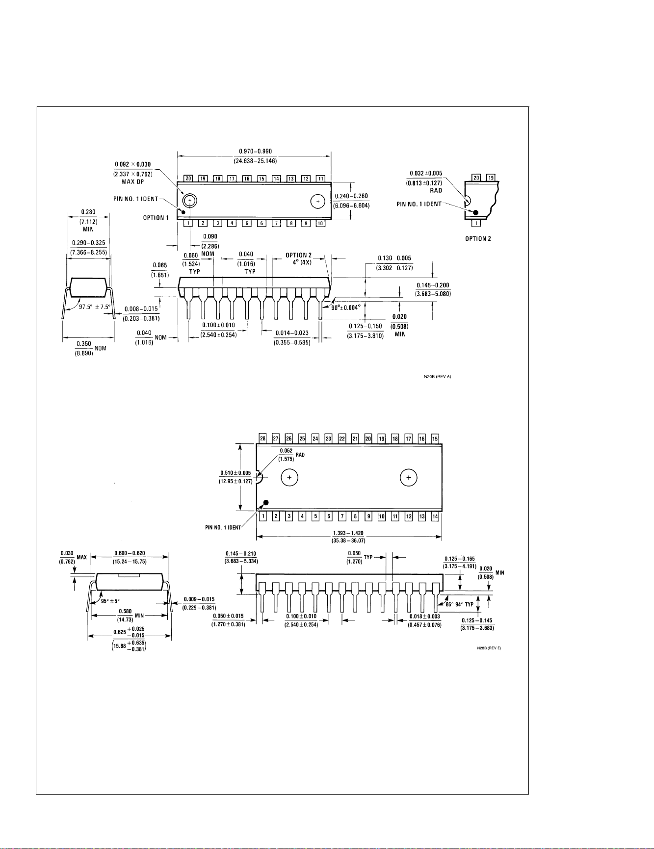
Physical Dimensions inches (millimeters) unless otherwise noted
Small Outline Molded Dual-In-Line Package (M)
Order Number COP882C-XXX/WM, COP982C-XXX/WM, COP682C-XXX/WM or COP982CH-XXX/WM
NS Package Number M20B
Small Outline Molded Dual-In-Line Package (M)
Order Number COP881C-XXX/WM, COP981C-XXX/WM, COP681C-XXX/WM or COP981CH-XXX/WM
NS Package Number M28B
COP880C
www.national.com 28
Physical Dimensions inches (millimeters) unless otherwise noted (Continued)
Molded Dual-In-Line Package (N)
Order Number COP882C-XXX/N, COP682C-XXX/N, COP982C-XXX/N or COP982CH-XXX/N
NS Package Number N20B
Molded Dual-In-Line Package (N)
Order Number COP881C-XXX/N, COP681C-XXX/N, COP981C-XXX/N or COP981CH-XXX/N
NS Package Number N28B
COP880C
www.national.com29

Physical Dimensions inches (millimeters) unless otherwise noted (Continued)
Molded Dual-In-Line Package (N)
Order Number COP880C-XXX/N, COP680C-XXX/N, COP980C-XXX/N or COP980CH-XXX/N
NS Package Number N40A
Plastic Leaded Chip Carrier (V)
Order Number COP880C-XXX/V, COP680C-XXX/V, COP980C-XXX/V or COP980CH-XXX/V
NS Package Number V44A
COP880C
www.national.com 30

Notes
LIFE SUPPORT POLICY
NATIONAL’S PRODUCTS ARE NOT AUTHORIZED FOR USE AS CRITICAL COMPONENTS IN LIFE SUPPORT
DEVICES OR SYSTEMS WITHOUT THE EXPRESS WRITTEN APPROVAL OF THE PRESIDENT AND GENERAL
COUNSEL OF NATIONAL SEMICONDUCTOR CORPORATION. As used herein:
1. Life support devices or systems are devices or
systems which, (a) are intended for surgical implant
into the body, or (b) support or sustain life, and
whose failure to perform when properly used in
accordance with instructions for use provided in the
labeling, can be reasonably expected to result in a
significant injury to the user.
2. A critical component is any component of a life
support device or system whose failure to perform
can be reasonably expected to cause the failure of
the life support device or system, or to affect its
safety or effectiveness.
National Semiconductor
Corporation
Americas
Email: support@nsc.com
National Semiconductor
Europe
Fax: +49 (0) 180-530 85 86
Email: europe.support@nsc.com
Deutsch Tel: +49 (0) 69 9508 6208
English Tel: +44 (0) 870 24 0 2171
Français Tel: +33 (0) 1 41 91 8790
National Semiconductor
Asia Pacific Customer
Response Group
Tel: 65-2544466
Fax: 65-2504466
Email: ap.support@nsc.com
National Semiconductor
Japan Ltd.
Tel: 81-3-5639-7560
Fax: 81-3-5639-7507
www.national.com
COP880C Microcontrollers
National does not assume any responsibility for use of any circuitry described, no circuit patent licenses are implied and National reserves the right at any time without notice to change said circuitry and specifications.

WWW.ALLDATASHEET.COM
Copyright © Each Manufacturing Company.
All Datasheets cannot be modified without permission.
This datasheet has been download from :
www.AllDataSheet.com
100% Free DataSheet Search Site.
Free Download.
No Register.
Fast Search System.
www.AllDataSheet.com
 Loading...