

National Semiconductor COP87LxxCJ, COP87LxxRJ Technical data
查询COP87L20CJ供应商
COP87LxxCJ/RJ Family
8-Bit CMOS OTP Microcontrollers with 4k or 32k Memory
and Comparator
General Description
The COP87LxxCJ/RJ Family OTP (One Time Programmable) microcontrollers are integrated COP8
devices with 4k or 32k memory, and an Analog comparator
(no brownout). These multi-chip CMOS devices are suited
for lower-functionality applications, and as pre-production
devices for a ROM design. Low cost, pin and software compatible (plus Brownout) 1k or2kROM versions are available
(COP820CJ/840CJ Family). Versions are available for use
with a range of COP8 software and hardware development
tools.
Family features include an 8-bit memory mapped architecture, 10 MHz CKI with 1µs instruction cycle, three clock op-
™
Base core
PRELIMINARY
September 1999
tions (-1=crystal; -2=external; -3=internal RC), one multifunction 16-bit timer/counter, MICROWIRE/PLUS
I/O, one analog comparator, power saving HALT mode with
multi-sourced wakeup/interrupt capability, on-chip R/C oscillator capacitor, high current outputs, software selectable I/O
options, WATCHDOG
Reset, program code security, 2.7V to 5.5V operation and
20/28 pin packages.
In this datasheet, the term COP87L20CJ refers to the
COP87L20CJ, and COP87L22CJ. COP840CJ refers to the
COP87L40CJ, COP87L42CJ, COP87L40RJ, and
COP87L42RJ.
Devices included in this datasheet are:
™
timer, modulator/timer, Power on
™
serial
COP87LxxCJ/RJ Family, 8-Bit CMOS OTP Microcontrollers with 4k or 32k Memory and
Comparator
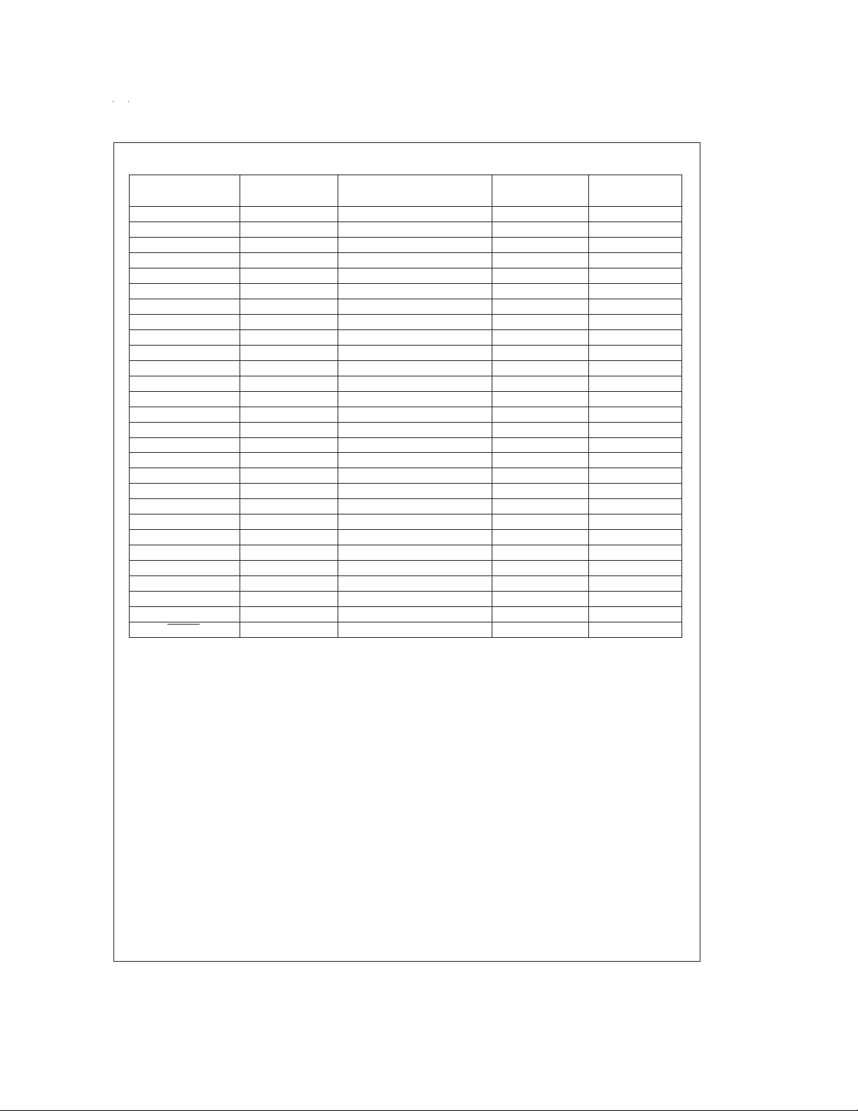
Device Memory (bytes) RAM (bytes) I/O Pins Packages Temperature
COP87L20CJ 4k OTP EPROM 64 24 28 DIP/SOIC -40 to +85˚C
COP87L22CJ 4k OTP EPROM 64 16 20 DIP/SOIC -40 to +85˚C
COP87L40CJ 4k OTP EPROM 128 24 28 DIP/SOIC -40 to +85˚C
COP87L42CJ 4k OTP EPROM 128 16 20 DIP/SOIC -40 to +85˚C
COP87L40RJ 32k OTP EPROM 128 24 28 DIP/SOIC -40 to +85˚C
COP87L42RJ 32k OTP EPROM 128 16 20 DIP/SOIC -40 to +85˚C
Key Features
n Multi-Input Wakeup (on the 8-bit Port L)
n Analog comparator
n Modulator/Timer (high speed PWM timer for IR
transmission)
n 16-bit multi-function timer supporting
— PWM mode
— External event counter mode
— Input capture mode
n Integrated capacitor for the R/C oscillator
n 4 or 32 kbyte on-board OTP EPROM with security
feature
n 64 or 128 bytes on-chip RAM
I/O Features
n Software selectable I/O options (TRI-STATE®, Push-Pull,
Weak Pull-Up Input, High Impedance Input)
n High current outputs (8 pins)
n Schmitt trigger inputs on Port G
n MICROWIRE/PLUS serial I/O
n Packages:
— 20 DIP/SO with 16 I/O pins
— 28 DIP/SO with 24 I/O pins
CPU/Instruction Set Features
n 1 µs instruction cycle time
n Three multi-source interrupts servicing
— External interrupt with selectable edge
— Timer interrupt
— Software interrupt
n Versatile and easy to use instruction set
n 8-bit stack pointer (SP) — stack in RAM
n Two 8-bit Register Indirect Data Memory Pointers (B and
X)
Fully Static CMOS
n Low current drain (typically<1 µA)
n Single supply operation: 2.7V to 5.5V
n Temperature range: −40˚C to +85˚C
Development Support
n Emulation device for the COP820CJ/COP840CJ
n Real time emulation and full program debug offered by
MetaLink Development Systems
TRI-STATE®is a registered trademark of National Semiconductor Corporation.
™
COP8
, MICROWIRE™, MICROWIRE/PLUS™and WATCHDOG™are trademarks of National Semiconductor Corporation.
®
iceMASTER
is a registered trademark of MetaLink Corporation.
© 1999 National Semiconductor Corporation DS012529 www.national.com
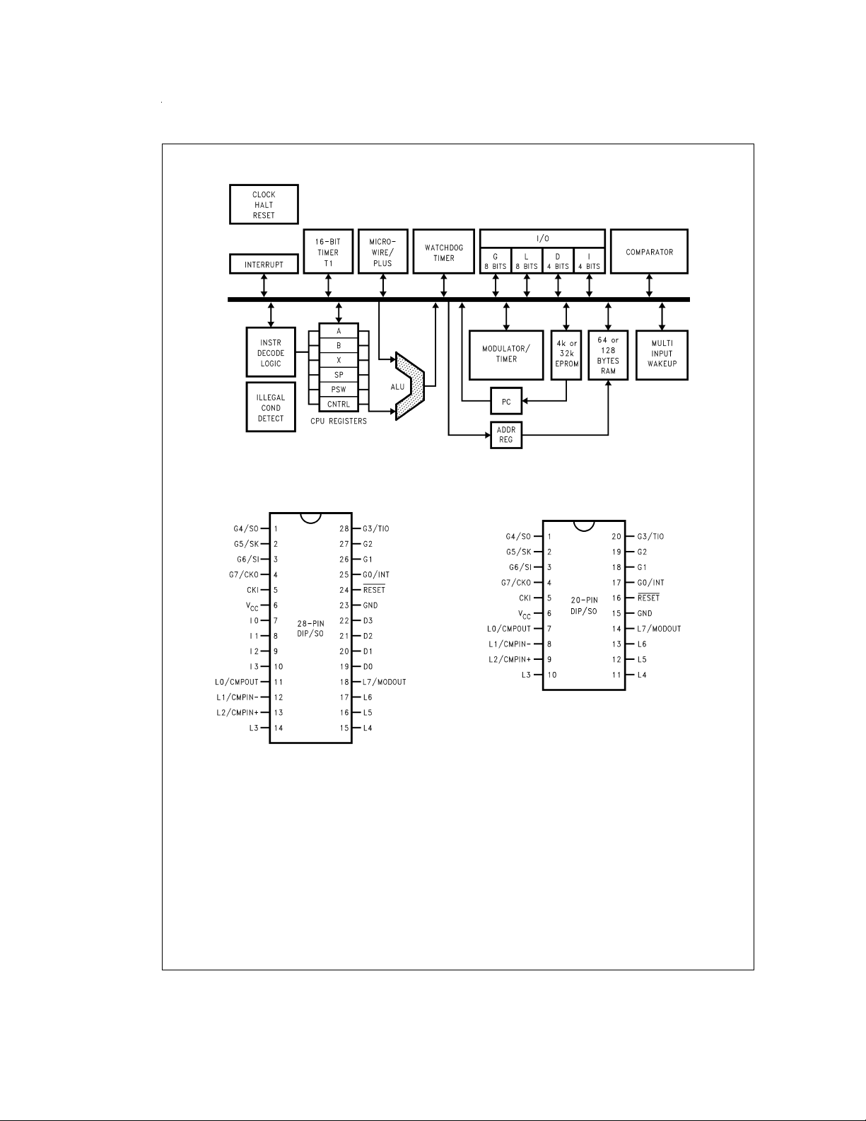
Block Diagram
Connection Diagrams
DS012529-1
FIGURE 1. Block Diagram
DS012529-2
Top View
Order Number
COP87L20CJN (-1N, -2N, -3N), or
COP87L20CJM(-1N, -2N, -3N), or
COP87L40CJN (-1N, -2N, -3N), or
COP87L40CJM (-1N, -2N, -3N), or
COP87L40RJN (-1N, -2N, -3N), or
COP87L40RJM (-1N, -2N, -3N)
See NS Package Number N28B or M28B
FIGURE 2. Connection Diagrams
Note: -1 Crystal Oscillator N - Brown out disabled
-2 External Oscillator
-3 R/C Oscillator
www.national.com 2
DS012529-3
Top View
Order Number
COP87L22CJN (-1N, -2N, -3N), or
COP87L22CJM(-1N, -2N, -3N), or
COP87L42CJN (-1N, -2N, -3N), or
COP87L42CJM (-1N, -2N, -3N), or
COP87L42RJN (-1N, -2N, -3N), or
COP87L42RJM (-1N, -2N, -3N)
See NS Package Number N20A or M20B
Pin Assignment
Port
Pin Funct. Pin Pin
L0 I/O MIWU/CMPOUT 7 11
L1 I/O MIWU/CMPIN− 8 12
L2 I/O MIWU/CMPIN+ 9 13
L3 I/O MIWU 10 14
L4 I/O MIWU 11 15
L5 I/O MIWU 12 16
L6 I/O MIWU 13 17
L7 I/O MIWU/MODOUT 14 18
G0 I/O INTR 17 25
G1 I/O 18 26
G2 I/O 19 27
G3 I/O TIO 20 28
G4 I/O SO 1 1
G5 I/O SK 2 2
G6 I SI 3 3
G7 I CKO 4 4
I0 I 7
I1 I 8
I2 I 9
I3 I 10
D0 O 19
D1 O 20
D2 O 21
D3 O 22
V
CC
GND 15 23
CKI 55
RESET
Typ
ALT 20 28
66
16 24
www.national.com3
Absolute Maximum Ratings (Note 1)
If Military/Aerospace specified devices are required,
please contact the National Semiconductor Sales Office/
Distributors for availability and specifications.
Supply Voltage (V
Voltage at any Pin −0.3V to V
) 7.0V
CC
CC
+ 0.3V
Total Current into V
pin (Source) 80 mA
CC
Total Current out of GND pin (sink) 80 mA
Storage Temperature Range −65˚C to +150˚C
Note 1:
Absolute maximum ratings indicate limits beyond which damage to
the device may occur. DC and AC electrical specifications are not ensured
when operating the device at absolute maximum ratings.
DC Electrical Characteristics
−40˚C ≤ TA≤ +85˚C unless otherwise specified
Parameter Conditions Min Typ Max Units
Operating Voltage 2.7 5.5 V
Power Supply Ripple 1 (Note 2) Peak to Peak 0.1 V
CC
Supply Current (Note 3)
CKI=10 MHz V
CKI=4 MHz V
CKI=4 MHz (COP87L20CJ) V
HALT Current (Note 4) V
INPUT LEVELS (V
IH,VIL
)
=
5.5V, tc=1µs 12 mA
CC
=
4.5V, tc=2.5 µs 6.5 mA
CC
=
4.0V, tc=2.5 µs 10 mA
CC
=
5.5V, CKI=0 MHz 12 µA
CC
Reset, CKI:
Logic High 0.8 V
Logic Low 0.2 V
CC
CC
All Other Inputs
Logic High 0.7 V
Logic Low 0.2 V
Hi-Z Input Leakage V
Input Pullup Current V
=
5.5V −2 +2 µA
CC
=
5.5V −40 −250 µA
CC
L- and G-Port Hysteresis (Note 7) 0.35 V
CC
CC
CC
Output Current Levels
D Outputs:
Source V
Sink (Note 5) V
L4–L7 Output Sink V
=
4.5V, V
CC
=
4.5V, V
CC
=
4.5V, V
CC
=
3.8V −0.4 mA
OH
=
1.0V 10 mA
OL
=
2.5V 15 mA
OL
All Others
Source (Weak Pull-up Mode) V
Source (Push-pull Mode) V
Sink (Push-pull Mode) V
(COP887L20CJ) V
=
4.5V, V
CC
=
4.5V, V
CC
=
4.5V, V
CC
=
5.5V, V
CC
=
3.2V −10 −110 µA
OH
=
3.8V −0.4 mA
OH
=
0.4V 1.6 mA
OL
=
0.4V
OL
TRI-STATE Leakage −2.0 +2.0 µA
Allowable Sink/Source
Current Per Pin
D Outputs 15 mA
L4–L7 (Sink) 20 mA
All Others 3mA
Maximum Input Current Room Temperature
±
100 mA
without Latchup (Note 6)
RAM Retention Voltage, V
r
500 ns Rise and 2.0 V
Fall Time (Min)
Input Capacitance 7pF
Load Capacitance on D2 1000 pF
Note 2: Rate of voltage change must be less than 10 V/mS.
Note 3: Supply current is measured after running 2000 cycles with a square wave CKI input, CKO open, inputs at rails and outputs open.
V
V
V
V
V
V
www.national.com 4
DC Electrical Characteristics (Continued)
Note 4: The HALT mode will stop CKI from oscillating in the RC and crystal configurations by bringing CKI high. HALT test conditions: L, and G0..G5 ports configured
as outputs and set high. The D port set to zero. All inputs tied to V
Note 5: The user must guarantee that D2 pin does not source more than 10 mA during RESET.If D2 sources more than 10 mA during reset, the device will go into
programming mode.
Note 6: Pins G6 and RESET are designed with a high voltage input network. These pins allow input voltages greater than V
to VCCwhen biased at voltages greater than VCC(the pins do not have source current when biased at a voltage below VCC). The effective resistance to VCCis 750Ω
(typical). These two pins will not latch up. The voltage at the pins must be limited to less than 14V.
. The comparator is disabled.
CC
and the pins will have sink current
CC
AC Electrical Characteristics
−40˚C ≤ TA≤ +85˚C unless otherwise specified
Parameter Conditions Min Typ Max Units
Instruction Cycle Time (tc)
Crystal/Resonator 4.5V ≤ V
R/C Oscillator 4.5V ≤ V
CKI Clock Duty Cycle (Note 7) fr=Max 40 60
Rise Time (Note 7) fr=10 MHz ext. Clock 12 ns
Fall Time (Note 7) fr=10 MHz ext. Clock 8 ns
Inputs
t
Setup
t
Hold
Output Propagation Delay R
t
PD1,tPD0
4.5V ≤ VCC≤ 5.5V 200 ns
4.5V ≤ VCC≤ 5.5V 60 ns
L
SO, SK 4.5V ≤ VCC≤ 5.5V 0.7 µs
All Others 4.5V ≤ V
Input Pulse Width
Interrupt Input High Time 1 tc
Interrupt Input Low Time 1 tc
Timer Input High Time 1 tc
Timer Input Low Time 1 tc
MICROWIRE
MICROWIRE Hold Time (t
™
Setup Time (t
)20ns
µWS
)56ns
µWH
MICROWIRE Output 220 ns
Propagation Delay (t
µPD
)
Reset Pulse Width 1 µs
Note 7: Parameter characterized but not production tested.
≤ 5.5V 1 DC µs
CC
≤ 5.5V 2 DC µs
CC
=
2.2k, CL=100 pF
≤ 5.5V 1 µs
CC
%
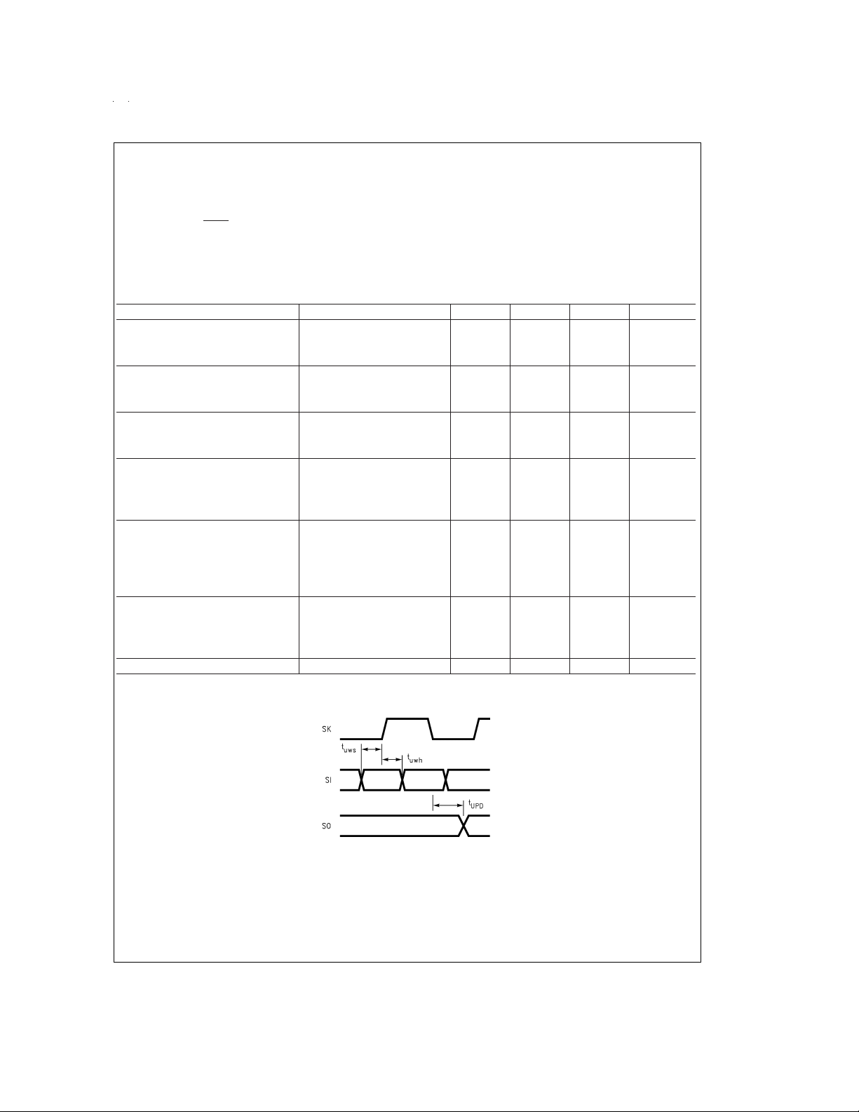
DS012529-4
FIGURE 3. MICROWIRE/PLUS Timing
www.national.com5
Pin Description
VCCand GND are the power supply pins.
CKI is the clock input. This can come from an external
source, a R/C generated oscillator or a crystal (in conjunction with CKO). See Oscillator description.
RESET is the master reset input. See Reset description.
PORT I is a 4-bit Hi-Z input port.
PORT L is an 8-bit I/O port.
There are two registers associated with the L port: a data
register and a configuration register. Therefore, each L I/O
bit can be individually configured under software control as
shown below:
Port L Port L Port L
Config. Data Setup
0 0 Hi-Z Input (TRI-STATE)
0 1 Input with Weak Pull-up
1 0 Push-pull Zero Output
1 1 Push-pull One Output
Three data memory address locations are allocated for this
port, one each for data register [00D0], configuration register
[00D1] and the input pins [00D2].
Port L has the following alternate features:
L7 MIWU or MODOUT (high sink current capability)
L6 MIWU (high sink current capability)
L5 MIWU (high sink current capability)
L4 MIWU (high sink current capability)
L3 MIWU
L2 MIWU or CMPIN+
L1 MIWU or CMPIN−
L0 MIWU or CMPOUT
The selection of alternate Port L functions is done through
registers WKEN [00C9] to enable MIWU and CNTRL2
[00CC] to enable comparator and modulator.
All eight L-pins have Schmitt Triggers on their inputs.
PORT G is an 8-bit port with 6 I/O pins (G0–G5) and 2 input
pins (G6, G7).
All eight G-pins have Schmitt Triggers on the inputs.
There are two registers associated with the G port: a data
register and a configuration register. Therefore each G port
bit can be individually configured under software control as
shown below:
Port G Port G Port G
Config. Data Setup
0 0 Hi-Z Input (TRI-STATE)
0 1 Input with Weak Pull-up
1 0 Push-pull Zero Output
1 1 Push-pull One Output
Three data memory address locations are allocated for this
port, one for data register [00D4], one for configuration register [00D5] and one for the input pins [00D6]. Since G6 and
G7 are Hi-Z input only pins, any attempt by the user to configure them as outputs by writing a one to the configuration
register will be disregarded. Reading the G6 and G7 configuration bits will return zeros. Note that the device will be
placed in the Halt mode by writing a “1” to the G7 data bit.
Six pins of Port G have alternate features:
G7 CKO crystal oscillator output (selected by mask option)
or HALT restart input/general purpose input (if clock
option is R/C or external clock)
G6 SI (MICROWIRE serial data input)
G5 SK (MICROWIRE clock I/O)
G4 SO (MICROWIRE serial data output)
G3 TIO (timer/counter input/output)
G0 INTR (an external interrupt)
Pins G2 and G1 currently do not have any alternate func-
tions.
The selection of alternate Port G functions are done through
registers PSW [00EF] to enable external interrupt and CNTRL1 [00EE] to select TIO and MICROWIRE operations.
PORT D is a four bit output port that is preset when RESET
goes low. One data memory address location is allocated for
the data register [00DC]. The user can tie two or more D port
outputs (except D2 pin) together in order to get a higher
drive.
Note: Care must be exercised with the D2 pin operation. At RESET, the ex-
ternal loads on this pin must ensure that the output voltages stay
above 0.8 V
keep the external loading on D2 to less than 1000 pF.
to prevent the chip from entering special modes. Also
CC
Functional Description
The internal architecture is shown in the block diagram. Data
paths are illustrated in simplified form to depict how the various logic elements communicate with each other in implementing the instruction set of the device.
ALU and CPU Registers
The ALU can do an 8-bit addition, subtraction, logical or shift
operations in one cycle time. There are five CPU registers:
A is the 8-bit Accumulator register
PC is the 15-bit Program Counter register
PU is the upper 7 bits of the program counter (PC)
PL is the lower 8 bits of the program counter (PC)
B is the 8-bit address register and can be auto incre-
mented or decremented.
X is the 8-bit alternate address register and can be auto
incremented or decremented.
SP is the 8-bit stack pointer which points to the subroutine
stack (in RAM).
B, X and SP registers are mapped into the on chip RAM. The
B and X registers are used to address the on chip RAM. The
SP register is used to address the stack in RAM during subroutine calls and returns. The SP must be initialized by software before any subroutine call or interrupts occurs.
Memory
The memory is separated into two memory spaces: program
and data.
PROGRAM MEMORY
Program memory consists of 4 kbytes of OTP EPROM.
These bytes of ROM may be instructions or constant data.
The memory is addressed by the 15-bit program counter
(PC). ROM can be indirectly read by the LAID instruction for
table lookup.
The device can be configured to inhibit external reads of the
program memory.This is done by programming the Security
Byte.
www.national.com 6
Memory (Continued)
SECURITY FEATURE
The memory array has an associate Security Byte that is located outside of the program address range. This byte can
be addressed only from programming mode by a programmer tool.
Security is an optional feature and can only be asserted after
the memory arrary has been programmed and verified.A secured part will read all 00(hex) by a programmer. The part
will fail Blank Check and will fail Verify operations. A Read
operation will fill the programmer’s memory with 00(hex).
The Security Byte itself is always readable with value of
00(hex) if unsecure and FF(hex) if secure.
DATA MEMORY
The data memory address space includes on chip RAM, I/O
and registers. Data memory is addressed directly by the instruction or indirectly through B, X and SP registers. The device has 128 bytes of RAM. Sixteen bytes of RAM are
mapped as “registers”, these can be loaded immediately,
decremented and tested. Three specific registers: X, B, and
SP are mapped into this space, the other registers are available for general usage.
Any bit of data memory can be directly set, reset or tested.
All I/O and registers (except A and PC) are memory mapped;
therefore, I/O bits and register bits can be directly and individually set, reset and tested, except the write once only bit
(WDREN, WATCHDOG Reset Enable), and the unused and
read only bits in CNTRL2 and WDREG registers.
Note: RAM contents are undefined upon power-up.
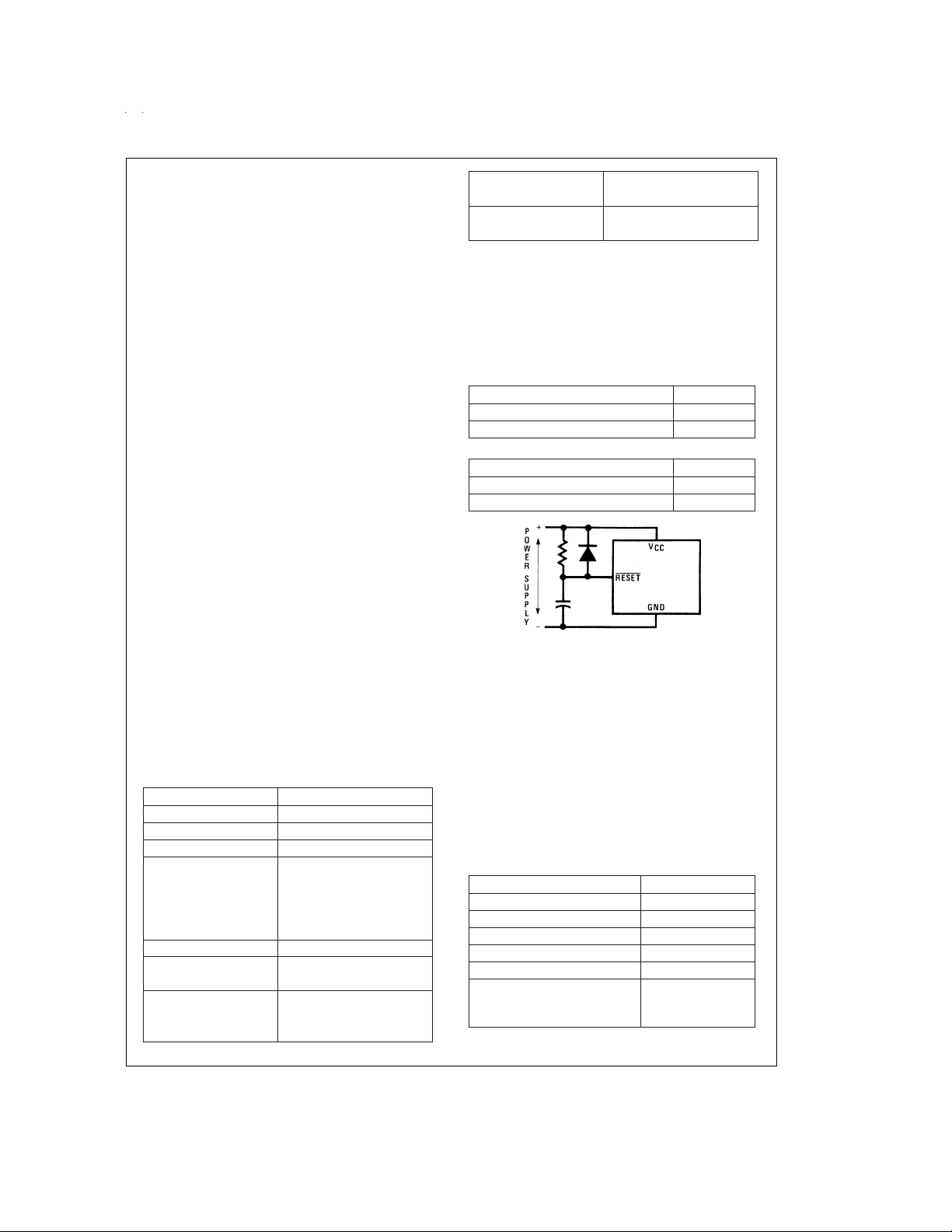
Reset
EXTERNAL RESET
The RESET input pin when pulled low initializes the
micro-controller.The user must insure that the RESET pin is
held low until V
the clock is stabilized. An R/C circuit with a delay 5x greater
than the power supply rise time is recommended (
The device immediately goes into reset state when the RESET input goes low. When the RESET pin goes high the device comes out of reset state synchronously. The device will
be running within two instruction cycles of the RESET pin going high. The following actions occur upon reset:
Port L TRI-STATE
Port G TRI-STATE
Port D HIGH
PC CLEARED
RAM Contents RANDOM with Power-On-
B, X, SP Same as RAM
PSW, CNTRL1, CNTRL2
and WDREG Reg. CLEARED
Multi-Input Wakeup Reg.
WKEDG, WKEN CLEARED
WKPND UNKNOWN
is within the specified voltage range and
CC
Figure 4
Reset
UNAFFECTED with external
Reset (power already
applied)
Data and Configuration
Registers forL&G CLEARED
WATCHDOG Timer Prescaler/Counter each
loaded with FF
The device comes out of the HALT mode when the RESET
pin is pulled low. In this case, the user has to ensure that the
RESET signal is low long enough to allow the oscillator to restart. An internal 256 t
with the two pin crystal oscillator. When the device comes
delay is normally used in conjunction
c
out of the HALT mode through Multi-Input Wakeup, this delay allows the oscillator to stabilize.
The following additional actions occur after the device
comes out of the HALT mode through the RESET pin.
If a two pin crystal/resonator oscillator is being used:
RAM Contents UNCHANGED
Timer T1 and A Contents UNKNOWN
WATCHDOG Timer Prescaler/Counter ALTERED
If the external or RC Clock option is being used:
RAM Contents UNCHANGED
Timer T1 and A Contents UNCHANGED
WATCHDOG Timer Prescaler/Counter ALTERED
RC>5 x Power Supply Rise Time
FIGURE 4. Recommended Reset Circuit
WATCHDOG RESET
With WATCHDOG enabled, the WATCHDOG logic resets
).
the device if the user program does not service the WATCHDOG timer within the selected service window. The WATCHDOG reset does not disable the WATCHDOG. Upon
WATCHDOG reset, the WATCHDOG Prescaler/Counter are
each initialized with FF Hex.
The following actions occur upon WATCHDOG reset that are
different from external reset.
WDREN WATCHDOG Reset Enable bit UNCHANGED
WDUDF WATCHDOG Underflow bit UNCHANGED
Additional initialization actions that occur as a result of
WATCHDOG reset are as follows:
Port L TRI-STATE
Port G TRI-STATE
Port D HIGH
PC CLEARED
Ram Contents UNCHANGED
B, X, SP UNCHANGED
PSW, CNTRL1 and CNTRL2
(except
WDUDF Bit) Registers CLEARED
DS012529-5
www.national.com7
Reset (Continued)
Multi-Input Wakeup Registers
WKEDG, WKEN CLEARED
WKPND UNKNOWN
Data and Configuration
Registers forL&G CLEARED
WATCHDOG Timer Prescalar/Counter
each loaded with FF
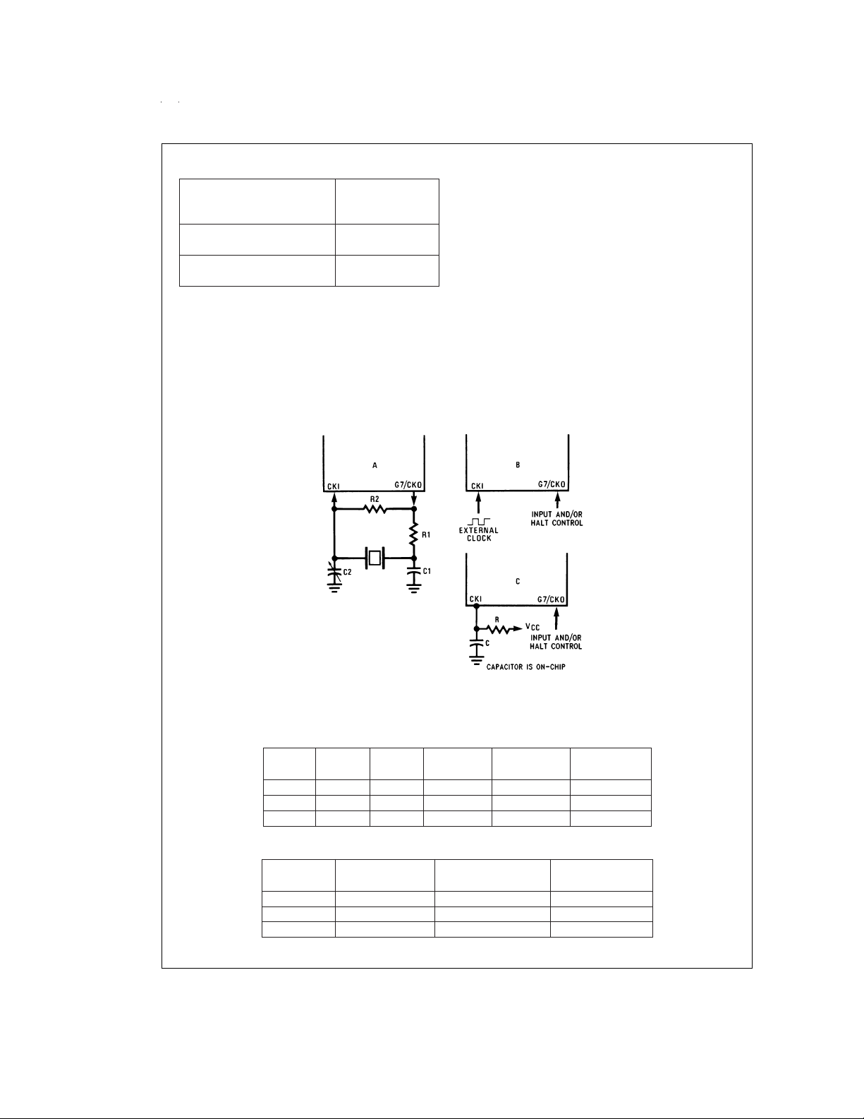
Oscillator Circuits
EXTERNAL OSCILLATOR
By selecting the external oscillator option, the CKI pin can be
driven by an external clock signal provided it meets the
specified duty cycle, rise and fall times, and input levels. The
G7/CKO is available as a general purpose input G7 and/or
HALT control.
CRYSTAL OSCILLATOR
By selecting the crystal oscillator option, the G7/CKO pin is
connected as a clock output, CKI and G7/CKO can be connected to make a crystal controlled oscillator.
the clock frequency for different component values. See
ure 5
for the connections.
Table1
shows
Fig-
R/C OSCILLATOR
By selecting R/C oscillator option, connecting a resistor from
the CKI pin to V
on-chip. The G7/CKO pin is available as a general purpose
makes a R/C oscillator. The capacitor is
CC
input G7 and/or HALT control. Adding an external capacitor
will jeopardize the clock frequency tolerance and increase
EMI emissions.
Table 2
shows the clock frequency for the different resistor
values. The capacitor is on-chip. See
Figure 5
for the
connections.
FIGURE 5. Clock Oscillator Configurations
TABLE 1. Crystal Oscillator Configuration
R1 R2 C1 C2 CKI Freq. Conditions
(kΩ)(MΩ) (pF) (pF) (MHz)
0 1 30 30–36 10 V
013030–36 4 V
5.6 1 100 100–156 0.455 V
TABLE 2. RC Oscillator Configuration (Part-To-Part Variation) T
R CK1 Freq. Instr. Cycle Conditions
(kΩ) (MHz) (µs)
±
8.2 3.3
2.2 1.3
3.9 0.75
www.national.com 8
%
10
±
%
10
±
%
10
3.0±10
7.7±10
13.3±10
DS012529-6
=
5V
CC
=
5V
CC
=
5V
CC
=
25˚C
A
%
%
%
=
V
5V
CC
=
V
5V
CC
=
V
5V
CC
Halt Mode
The device is a fully static device. The device enters the
HALTmode by writing a one to the G7 bit of the G data register. Once in the HALT mode, the internal circuitry does not
receive any clock signal and is therefore frozen in the exact
state it was in when halted. In this mode the chip will only
draw leakage current.
The device supports three different methods of exiting the
HALT mode. The first method is with a low to high transition
on the CKO (G7) pin. This method precludes the use of the
crystal clock configuration (since CKO is a dedicated output). It may be used either with an RC clock configuration or
an external clock configuration. The second method of exiting the HALTmode is with the multi-Input Wakeup feature on
the L port. The third method of exiting the HALT mode is by
pulling the RESET input low.
If the two pin crystal/resonator oscillator is being used and
Multi-Input Wakeup causes the device to exit the HALT
mode, the WAKEUP signal does not allow the chip to start
running immediately since crystal oscillators have a delayed
start up time to reach full amplitude and freuqency stability.
The WATCHDOG timer (consisting of an 8-bit prescaler followed by an 8-bit counter) is used to generate a fixed delay
of 256tc to ensure that the oscillator has indeed stabilized
before allowing instruction execution. In this case, upon detecting a valid WAKEUP signal only the oscillator circuitry is
enabled. The WATCHDOG Counter and Prescaler are each
loaded with a value of FF Hex. The WATCHDOGprescaler is
clocked with the tc instruction cycle. (The tc clock is derived
by dividing the oscillator clock down by a factor of 10).
The Schmitt trigger following the CKI inverter on the chip ensures that the WATCHDOG timer is clocked only when the
oscillator has a sufficiently large amplitude to meet the
Schmitt trigger specs. This Schmitt trigger is not part of the
oscillator closed loop. The start-up timeout from the WATCHDOG timer enables the clock signals to be routed to the rest
of the chip. The delay is not activated when the device
comes out of HALT mode through RESET pin. Also, if the
clock option is either RC or External clock, the delay is not
used, but the WATCHDOG Prescaler/-Counter contents are
changed. The Development System will not emulate the
256tc delay.
The RESET pin will cause the device to reset and start executing from address X’0000. A low to high transition on the
G7 pin (if single pin oscillator is used) or Multi-Input Wakeup
will cause the device to start executing from the address following the HALT instruction.
When RESET pin is used to exit the device from the HALT
mode and the two pin crystal/resonator (CKI/CKO) clock option is selected, the contents of the Accumulator and the
Timer T1 are undetermined following the reset. All other information except the WATCHDOG Prescaler/Counter contents is retained until continuing. All information except the
WATCHDOG Prescaler/Counter contents is retained if the
device exits the HALT mode through G7 pin or Multi-Input
Wakeup.
G7 is the HALT-restartpin, but it can still be used as an input.
If the device is not halted, G7 can be used as a general purpose input.
Note: Toallowclockresynchronization,itis necessary to program two NOP’s
immediately after the device comes out of the HALT mode. The user
must program two NOP’s following the “enter HALT mode” (set G7
data bit) instruction.
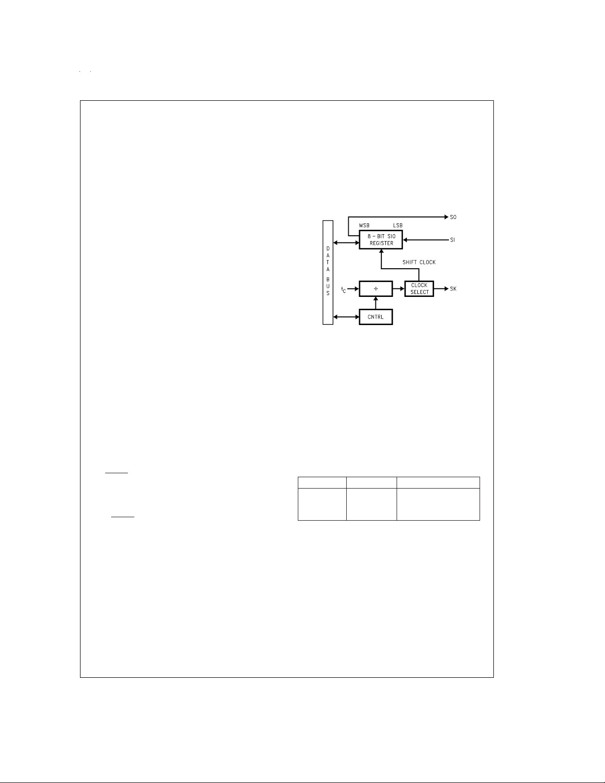
MICROWIRE/PLUS
MICROWIRE/PLUS is a serial synchronous bidirectional
communications interface. The MICROWIRE/PLUS capability enables the device to interface with any of National Semiconductor’s MICROWIRE peripherals (i.e. A/D converters,
display drivers, EEPROMS, etc.) and with other microcontrollers which support the MICROWIRE/PLUS interface. It
consists of an 8-bit serial shift register (SIO) with serial data
input (SI), serial data output (SO) and serial shift clock (SK).
Figure 6
shows the block diagram of the MICROWIRE/PLUS
interface.
DS012529-7
FIGURE 6. MICROWIRE/PLUS Block Diagram
The shift clock can be selected from either an internal source
or an external source. Operating the MICROWIRE/PLUS interface with the internal clock source is called the Master
mode of operation. Operating the MICROWIRE/PLUS interface with an external shift clock is called the Slave mode of
operation.
The CNTRL register is used to configure and control the
MICROWIRE/PLUS mode. To use the MICROWIRE/PLUS ,
the MSEL bit in the CNTRL register is set to one. The SK
clock rate is selected by the two bits, SL0 and SL1, in the
CNTRL register.
may be selected.
SL1 SL0 SK Cycle Time
00 2t
01 4t
1x 8t
where,
is the instruction cycle time.
t
c
MICROWIRE/PLUS OPERATION
Setting the BUSY bit in the PSW register causes the
MICROWIRE/PLUS arrangement to start shifting the data. It
gets reset when eight data bits have been shifted. The user
may reset the BUSY bit by software to allow less than 8 bits
to shift. The device may enter the MICROWIRE/PLUS mode
either as a Master or as a Slave.
vice microcontrollers and several peripherals may be interconnected using the MICROWIRE/PLUS arrangement.
Master MICROWIRE/PLUS Operation
In the MICROWIRE/PLUS Master mode of operation the
shift clock (SK) is generated internally by the device. The
MICROWIRE/PLUS Master always initiates all data ex-
Table3
details the different clock rates that
TABLE 3.
Figure 7
shows how two de-
c
c
c
www.national.com9
 Loading...