


查询COP87L88EB Family供应商
COP87L88EB/RB Family
8-Bit CMOS OTP Microcontrollers with 16k or 32k
Memory, CAN Interface, 8-Bit A/D, and USART
General Description
The COP87L88EB/RB Family OTP (One Time programmable) microcontrollers are highly integrated COP8
ture core devices with 16k or 32k memory and advanced
features including a CAN 2.0B (passive) interface, A/D and
USART. Thesemulti-chipCMOS devices are suited for applications requiring a full featured controller with a CAN interface, low EMI, and versatile communications interfaces, and
as pre-production devices for ROM designs. Pin and software compatible 8k ROM versions (COP888EB) are available as well as a range of COP8 software and hardware development tools.
COP87L88EB/RB Family, 8-Bit CMOS OTP Microcontrollers with 16k or 32k Memory, CAN
Interface, 8-Bit A/D, and USART
July 1999
Features include an 8-bit memory mapped architecture, 10
MHz CKI (-XE=crystal oscillator) with 1µs instruction cycle,
™
two multi-function 16-bit timer/counters, WATCHDOG and
Fea-
clock monitor, idle timer, CAN 2.0B (passive) interface,
MICROWIRE/PLUS
fully buffered USART, 8 bit A/D with 8 channels, two power
saving HALT/IDLE modes, MIWU, software selectable I/O
options, low EMI 4.5V to 5.5V operation, program code security, and 44/68 pin packages.
Note: A companion device with CAN interface, less I/O and
memory,A/D, and PWM timer is the COP87L84BC.
Devices included in this datasheet are:
™
serial I/O, SPI master/slave interface,
Device Memory (bytes) RAM (bytes) I/O Pins Packages Temperature
COP87L88EB 16k OTP EPROM 192 35 44 PLCC -40 to +85˚C
COP87L89EB 16k OTP EPROM 192 58 68 PLCC -40 to +85˚C
COP87L88RB 32k OTP EPROM 192 35 44 PLCC -40 to +85˚C
COP87L89RB 32k OTP EPROM 192 58 68 PLCC -40 to +85˚C
Key Features
n CAN 2.0B (passive) bus interface, with Software Power
save mode
n 8-bit A/D Converter with 8 channels
n Fully buffered USART
n Multi-input wake up (MIWU) on both Port L and M
n SPI Compatible Master/Slave Interface
n 16 or 32 kbytes of on-board OTP EPROM with security
feature
Note: Mask ROMed device with equivalent on-chip features and program
memory size of 8k is available.
n 192 bytes of on-board RAM
Additional Peripheral Features
n Idle timer (programmable)
n Two 16-bit timer, with two 16-bit registers supporting
— Processor independent PWM mode
— External Event counter mode
— Input capture mode
n WATCHDOG
n MICROWIRE/PLUS serial I/O
™
and Clock Monitor
I/O Features
n Software selectable I/O options (TRI-STATE®outputs,
Push pull outputs, Weak pull up input, High impedance
input)
n Schmitt trigger inputs on Port G, L and M
n Packages: 44 PLCC with 35 I/O pins;
68 PLCC with 58 I/O pins
TRI-STATE®is a registered trademark of National Semiconductor Corporation.
™
COP8
, MICROWIRE/PLUS™, WATCHDOG™and MICROWIRE™are trademarks of National Semiconductor Corporation.
®
iceMASTER
is a registered trademark of MetaLink Corporation.
© 1999 National Semiconductor Corporation DS100044 www.national.com
CPU/Instruction Set Features
n 1 µs instruction cycle time
n Fourteen multi-sourced vectored interrupts servicing
— External interrupt
— Idle Timer T0
— Timers (T1 and T2) (4 Interrupts)
— MICROWIRE/PLUS and SPI
— Multi-input Wake up
— Software Trap
— CAN interface (3 interrupts)
— USART (2 Inputs)
n Versatile easy to use instruction set
n 8-bit stacker pointer (SP) (Stack in RAM)
n Two 8-bit RegisterR Indirect Memory Pointers (B, X)
Fully Static CMOS
n Two power saving modes: HALT, IDLE
n Single supply operation: 4.5V to 5.5V
n Temperature range: −40˚C to +85˚C
Development Support
n Emulation device for COP888EB
n Real time emulation and full program debug offered by
MetaLink Development System

Basic Functional Description
n CAN I/F —CAN serial bus interface block as described
in the CAN specification part 2.0B (Passive)
— Interface rates up to 250k bit/s are supported utilizing
standard message identifiers
n Programmable double buffered USART
n A/D— 8-bit, 8 channel, 1-LSB Resolution, with improved
Source Impedance and improved channel to channel
cross talk immunity
n Multi-Input-Wake-Up (MIWU) — edge selectable wake-up
and interrupt capability via input port and CAN interface
(Port L, Port M and CAN I/F); supports Wake-Up
capability on SPI, USART, and T2
n Port C —8-bit bi-directional I/O port
n Port D —8-bit Output port with high current drive
capability (10 mA)
n Port F —8-bit bidirectional I/O
n Port G —8-bit bidirectional I/O port, including alternate
functions for:
— MICROWIRE
— Timer 1 Input or Output (Depending on mode
selected)
— External Interrupt input
— WATCHDOG Output
n Port I —8-bit input port combining either digital input, or
up to eight A/D input channels
n Port L —8-bit bidirectional I/O port, including alternate
functions for:
— USART Transmit/Receive I/O
— Multi-input-wake up (MIWU on all pins)
n Port M —8-bit I/O port, with the following alternate
function
— SPI Interface
— MIWU
™
Input and Output
— CAN Interface Wake-up (MSB)
— Timer 2 Input or Output (Depending on mode
selected)
n Port N —8-bit bidirectional I/O
— SPI Slave Select Expander
n Two 16-bit multi-function Timer counters (T1 and T2)
plus supporting registers
— (I/P Capture, PWM and Event Counting)
n Idle timer —Provides a basic time-base counter, (with
interrupt) and automatic wake up from IDLE mode
programmable
n MICROWIRE/PLUS— MICROWIRE serial peripheral
interface, supporting both Master and Slave operation
n HALT and IDLE — Software programmable low current
modes
— HALT— Processor stopped, Minimum current
— IDLE— Processor semi-active more than 60%power
saving
n 16 or 32 kbytes OTP EPROM and 192 bytes of on
board static RAM
n SPI Master/Slave interface includes 12 bytes Transmit
and 12 bytes Receive FIFO Buffers. Operates up to 1M
Bit/S
n On board programmable WATCHDOG and CLOCK
Monitor
Applications
n Automobile Body Control and Comfort System
n Integrated Driver Informaiton Systems
n Steering Wheel Control
n Car Radio Control Panel
n Sensor/Actuator Applications in Automotive and
Industrial Control
Block Diagram
FIGURE 1. Block Diagram
www.national.com 2
DS100044-1
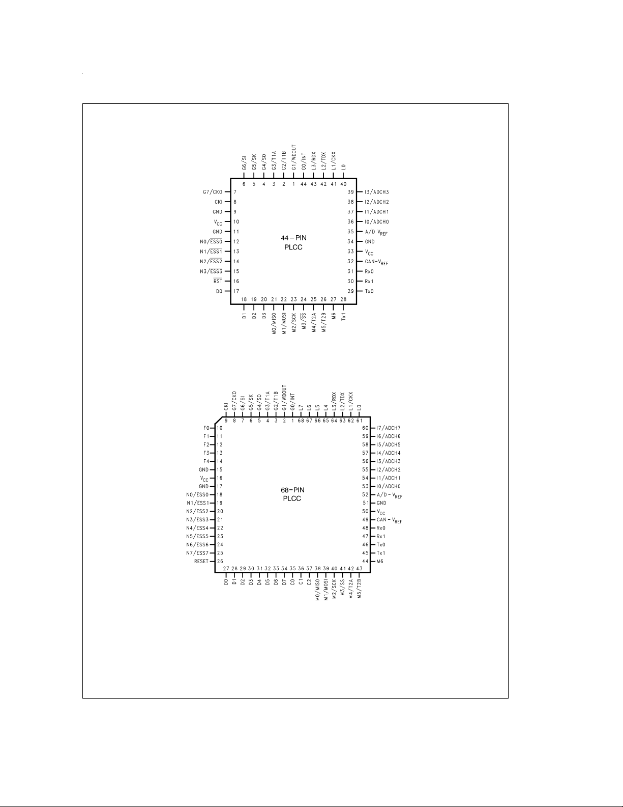
Connection Diagrams
Order Number COP87L88EBV-XE or COP87L88RBV-XE
Plastic Chip Carrier
DS100044-2
Top View
See NS Plastic Chip Package Number V44A
Plastic Leaded Chip Carrier
Note:
-X Crystal Oscillator
-E Halt Mode Enabled
DS100044-3
Top View
Order Number COP87L89EBV-XE or COP87L89RBV-XE
See NS Plastic Chip Package Number V68A
FIGURE 2. Connection Diagrams
www.national.com3
Connection Diagrams (Continued)
Pinouts for 44-Pin and 68-Pin Packages
Port Type ALT 44-Pin 68-Pin
Pin Function PLCC PLCC
G0 I/O INT 44 1
G1 I/O WDOUT 1 2
G2 I/O T1B 2 3
G3 I/O T1A 3 4
G4 I/O SO 4 5
G5 I/O SK 5 6
G6 I SI 6 7
G7 I CKO 7 8
D0 O 17 27
D1 O 18 28
D2 O 19 29
D3 O 20 30
D4 O 31
D5 O 32
D6 O 33
D7 O 34
I0 I ADCH0 36 53
I1 I ADCH1 37 54
I2 I ADCH2 38 55
I3 I ADCH3 39 56
I4 I ADCH4 57
I5 I ADCH5 58
I6 I ADCH6 59
I7 I ADCH7 60
L0 I/O MIWU 40 61
L1 I/O MIWU;CKX 41 62
L2 I/O MIWU;TDX 42 63
L3 I/O MIWU;RDX 43 64
L4 I/O MIWU 65
L5 I/O MIWU 66
L6 I/O MIWU 67
L7 I/O MIWU 68
M0 I/O MIWU;MISO 21 38
M1 I/O MIWU;MOSI 22 39
M2 I/O MIWU;SCK 23 40
M3 I/O MIWU;SS
M4 I/O MIWU;T2A 25 42
M5 I/O MIWU;T2B 26 43
M6 I/O MIWU 27 44
N0 I/O ESS0 12 18
N1 I/O ESS1 13 19
N2 I/O ESS2 14 20
N3 I/O ESS3 15 21
N4 I/O ESS4 22
N5 I/O ESS5 23
N6 I/O ESS6 24
N7 I/O ESS7 25
24 41
Port Type ALT 44-Pin 68-Pin
Pin Function PLCC PLCC
F0 I/O 10
F1 I/O 11
F2 I/O 12
F3 I/O 13
F4 I/O 14
C0 I/O 35
C1 I/O 36
C2 I/O 37
RX0 I 31 48
RX1 I 30 47
TX0 O 29 46
TX1 O 28 45
CANV
REF
32 49
CKI 8 9
RESET 16 26
DV
CC
10, 33 16, 50
GND 9, 11, 34 15, 17,
51
A/D
V
REF
35 52
www.national.com 4

Absolute Maximum Ratings (Note 1)
If Military/Aerospace specified devices are required,
please contact the National Semiconductor Sales Office/
Distributors for availability and specifications.
Supply Voltage (V
Voltage at Any Pin −0.3V to V
)6V
CC
CC
+0.3V
Total Current into V
Pins (Source) 90 mA
CC
Total Current out of GND Pins (Sink) 100 mA
Storage Temperature Range −65˚C to +150˚C
Note 1: Absolute maximum ratings indicate limits beyond which damage to
the device may occur. DC and AC electrical specifications are not ensured
when operating the device at absolute maximum ratings.
DC Electrical Characteristics
−40˚C ≤ TA≤ +85˚C
Parameter Conditions Min Typ Max Units
Operating Voltage 4.5 5.5 V
Power Supply Ripple (Note 2) Peak-to-Peak 0.1 V
Supply Current V
= 5.5V, tc=1µs 16 mA
CC
CC
CKI = 10 MHz (Note 3)
HALT Current (Notes 4, 5) V
IDLE Current (Note 5) V
= 5.5V, CKI=0MHz
CC
= 5.5V, tc= 1 µs 5.5 mA
CC
<
1µA
CKI = 10 MHz
Input Levels (V
IH,VIL
)
Reset, CKI
Logic High 0.8V
Logic Low 0.2V
CC
CC
All Other Inputs
Logic High 0.7V
Logic Low 0.2V
Hi-Z Input Leakage V
Input Pull-Up Current V
= 5.5V
CC
= 5.5V, VIN= 0V −40 −250 µA
CC
Port G, L and M Input Hysteresis (Note 8) 0.05V
CC
CC
±
2µA
CC
Output Current Levels
D Outputs
Source V
Sink V
= 4.5V, VOH= 3.3V −0.4 mA
CC
= 4.5V, VOL= 1.0V 10 mA
CC
CAN Transmitter Outputs
Source (Tx1) V
Sink (Tx0) V
= 4.5V, VOH=VCC−0.1V −1.5 mA
CC
V
= 4.5V, VOH=VCC− 0.6V −10 +5.0 mA
CC
= 4.5V, VOL= 0.1V 1.5 mA
CC
V
= 4.5V, VOL= 0.6V 10 mA
CC
All Others
Source (Weak Pull-Up) V
Source (Push-Pull) V
Sink (Push-Pull) V
TRI-STATE Leakage V
= 4.5V, VOH= 2.7V −10 −110 µA
CC
= 4.5V, VOH= 3.3V −0.4 mA
CC
= 4.5V, VOL= 0.4V 1.6 mA
CC
CC
= 5.5V
±
2.0 µA
Allowable Sink/Source Current per Pin
D Outputs (sink) 15 mA
Tx0 (Sink) (Note 8) 30 mA
Tx1 (Source) (Note 8) 30 mA
All Other 3mA
Maximum Input Current Room Temp
±
200 mA
without Latchup (Notes 6, 8)
RAM Retention Voltage, V
(Note 7) 500 ns Rise and Fall Time 2.0 V
r
Input Capacitance (Note 8) 7 pF
Load Capacitance on D2 1000 pF
Note 2: Maxiumum rate of voltage change must be<0.5V/ms
V
V
V
V
V
V
www.national.com5
DC Electrical Characteristics (Continued)
Note 3: Supply current is measured after running 2000 cycles with a square wave CKI input, CKO open, inputs at VCCor GND, and outputs open.
Note 4: The HALT mode will stop CKI from oscillating in the Crystal configurations. Halt test conditions: All inputs tied to V
figured as outputs and programmed low; D outputs programmed high. Parameter refers to HALT mode entered via setting bit 7 of the Port G data register. Part will
pull up CKI during HALT in crystal clock mode. Both CAN main comparator and the CAN Wakeup comparator need to be disabled.
Note 5: . HALTand IDLE current specifications assume CAN block comparators are disabled.
Note 6: Pins G6 and RESET are designed with a high voltage input network. These pins allow input voltages greater than V
to VCCwhen biased at voltages greater than VCC(the pins do not have source current when biased at a voltage below VCC). The effective resistance to VCCis 750Ω
(typical). These two pins will not latch up. The voltage at the pins must be limited to less than 14V.
Note 7: Condition and parameter valid only for part in HALT mode.
Note 8: Parameter characterized but not tested.
; Port C, G, E, F, L, M and N I/Os con-
CC
and the pins will have sink current
CC
AC Electrical Characteristics
−40˚C ≤ TA≤ +85˚C
Parameter Conditions Min Typ Max Units
Instruction Cycle Time (t
Crystal/Resonator V
Inputs
t
SETUP
t
HOLD
Output Propagation Delay (t
SK, SO V
All others V
MICROWIRE
Setup Time (tUWS) (Note 10) 20 ns
Hold Time (tUWH) (Note 10) 56 ns
Output Pop Delay (tUPD) 220 ns
Input Pulse Width
Interrupt High Time 1 t
Interrupt Low Time 1t
Timer 1, 2 High Time 1 t
Timer 1, 2 Low Time 1 t
Reset Pulse Width (Note 10) 1.0 µs
tc= Instruction Cycle Time
The maximum bus speed achievable with the CAN interface is a function of crystal frequency,message length and software overhead. The device can support a bus
speed of up to 1 Mbit/S with a 10 MHz oscillator and 2 byte messages. The 1M bus speed refers to the rate at which protocol and data bits are transferred on the
bus. Longer messages require slower bus speeds due to the time required for software intervention between data bytes. The device will support a maximum of 125k
bits/s with eight byte messages and a 10 MHz oscillator.
For device testing purpose of all AC parameters, V
Note 9: The output propagation delay is referenced to the end of the instruction cycle where the output change occurs.
Note 10: Parameter not tested.
)
c
≥ 4.5V 1.0 DC µs
CC
VCC≥ 4.5V 200 ns
VCC≥ 4.5V 60 ns
) (Note 9) CL= 100 pF, RL= 2.2 kΩ
PD1,tPD0
will be tested at 0.5*VCC.
OH
≥ 4.5V 0.7 µs
CC
≥ 4.5V 1 µs
CC
c
c
c
c
On-Chip Voltage Reference
−40˚C ≤ TA≤ +85˚C
Parameter Conditions Min Max Units
<
Reference Voltage I
V
REF
Reference Supply I
Current, I
DD
Note 11: Reference supply IDDis supplied for information purposes only, it is not tested.
www.national.com 6
80 µA, 0.5VCC−0.12 0.5VCC+0.12 V
OUT
VCC=5V
= 0A, (No Load) 120 µA
OUT
VCC= 5V (Note 11)

CAN Comparator DC and AC Characteristics
4.8V ≤ VCC≤ 5.2V, −40˚C ≤ TA≤ +85˚C
Parameter Conditions Min Typ Max Units
±
Differential Input Voltage
<
Input Offset Voltage 1.5V
V
<
IN
VCC−1.5V
Input Common Mode 1.5 V
25 mV
±
10 mV
−1.5 V
CC
Voltage Range
Input Hysteresis 8 mV
A/D Converter Specifications
(4.5V ≤ VCC≤ 5.5V) (VSS− 0.050V) ≤ Any Input ≤ (VCC+ 0.050V)
Parameter Conditions Min Typ Max Units
Resolution 8 Bits
Absolute Accuracy V
REF=VCC
Non-Linearity
Deviation from the Best Straight Line
Differential Non-Linearity
Common Mode Input Range (Note 14) GND V
DC Common Mode Error
Off Channel Leakage Current 1 2.0 µA
On Channel Leakage Current 1 2.0 µA
A/D Clock Frequency (Note 13) 0.1 1.67 MHz
Conversion Time (Note 12) 17 A/D Clock Cycles
Internal Reference Resistance Turn-On Time (Note 15) 1 µs
Note 12: Conversion Time includes sample and hold time.
Note 13: See Prescaler description.
Note 14: For V
input voltages below ground or above the V
to conduct — especially at elevated temperatures, and cause errors for analog inputs near full-scale. The spec allows 50 mV forward bias of either diode.This means
that as long as the analog V
voltage range will therefore require a minimum supply voltage of 4.950 V
Note 15: Time for internal reference resistance to turn on after coming out of Halt or Idle Mode.
(−)=VIN(+) the digital output code will be 0000 0000. Two on-chip doides are ties to each analog input. The diodes will forward conduct for analog
IN
does not exceed the supply voltage by more than 50 mV, the output code will be correct. To achieve an absolute 0 VDCto 5 VDCinput
IN
supply.Be careful, during testing at low VCClevels (4.5V), as high level analog inputs (5V) can cause this input diode
CC
over temperature variations, initial tolerance and loading.
DC
±
2 LSB
±
1 LSB
±
1 LSB
CC
±
0.5 LSB
V
DS100044-4
FIGURE 3. MICROWIRE/PLUS Timing Diagram
DS100044-5
FIGURE 4. SPI Timing Diagram
www.national.com7
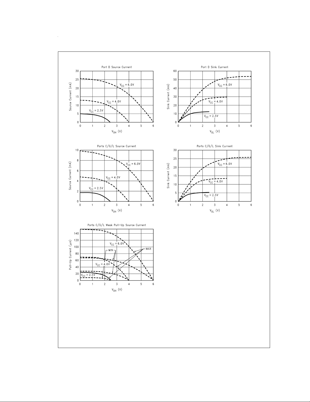
Typical Performance Characteristics (−55˚C ≤ T
DS100044-57 DS100044-58
A
=
+125˚C)
DS100044-59 DS100044-60
DS100044-61
www.national.com 8
Pin Description
VCCand GND are the power supply pins.
CKI is the clock input. The clock can come from a crystal os-
cillator (in conjunction with CKO). See Oscillator Description
section.
RESET is the master reset input. See Reset Descriptionsection.
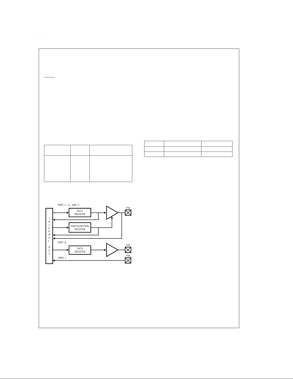
The device contains seven bidirectional 8-bit I/O ports (C, E,
F, G, L, M, N) where each individual bit may be independently configured as an input (Schmitt trigger inputs on all
ports), output or TRI-STATE under program control. Three
data memory address locations are allocated for each of
these I/O ports. Each I/O port has two associated 8-bit
memory mapped registers, the CONFIGURATION register
and the output DATAregister.A memory mapped address is
also reserved for the input pins of each I/O port. (See the
memory map for the various addresses associated with the
I/O ports.)
device. The DATA and CONFIGURATION registers allow for
each port bit to be individually configured under software
control as shown below:
Port L and M are 8-bit I/O ports, they support Multi-Input
Wake-up (MIWU) on all eight pins. All L-pins and M-pins
have Schmitt triggers on the inputs.
Port L and M only have one (1) interrupt vector.
Port L has the following alternate features:
Figure 5
shows the I/O port configurations for the
Configuration Data Port Set-Up
Register Register
0 0 Hi-Z Input
(TRI-STATE Output)
0 1 Input with Weak Pull-Up
1 0 Push-Pull Zero Output
1 1 Push-Pull One Output
FIGURE 5. I/O Port Configurations
L7 MIWU
L6 MIWU
L5 MIWU
L4 MIWU
L3 MIWU or RDX
L2 MIWU or TDX
L1 MIWU or CKX
L0 MIWU
DS100044-6
Port G is an 8-bit port with 5 I/O pins (G0–G5), an input pin
(G6), and one dedicated output pin (G7). Pins G0–G6 all
have Schmitt Triggers on their inputs. G7 serves as the dedicated output pin for the CKO clock output.There are two registers associated with the G Port, a data register and a configuration register. Therefore, each of the 6 I/O bits (G0–G5)
can be individually configured under software control.
Since G6 is an input only pin and G7 is the dedicated CKO
clock output pin the associated bits in the data and configuration registers for G6 and G7 are used for special purpose
functions as outlined below. Reading the G6 and G7 data
bits will return zeroes.
Note that the chip will be placed in the HALT mode by wirting
a ’’1” to bit 7 of the Port G Data Register. Similarly the chip
will be placed in the IDLE mode by writing a “1” to bit 6 of the
Port G Data Register.
Writing a “1” to bit 6 of the Port G Configuration Register enables the MICROWIRE/PLUS to operate with the alternate
phase of the SK clock
Config. Reg. Data Reg.
G7 CLKDLY HALT
G6 Alternate SK IDLE
Port G has the following alternate features:
G6 SI (MICROWIRE Serial Data Input)
G5 SK (MICROWIRE Serial Clock)
G4 SO (MICROWIRE Serial Data Output)
G3 T1A (Timer I/O)
G2 (Timer T1 Capture Input)
G1 Dedicated WATCHDOG output
G0 INTR (External Interrupt Input)
Port G has the following dedicated function:
G7 CKO Oscillator dedicated output
Port M is a bidirectional I/O, it may be configured in software
as Hi-Z input, weak pull-up, or push-pull output. These pins
may be used as general purpose input/output pins or for selected altlernate functions.
Port M pins have optional alternate functions. Each pin
(M0–M5) has been assigned an alternate data, configuration, or wakeup source. If the respective alternate function is
selected the content of the associated bits in the configuration and/or data register are ignored. If an alternate wakeup
source is selected the input level at the respective pin will be
ignored for the purpose of triggering a wakeup event, however it will still be possible to read that pin by accessing the
input register.The SPI (Serial Peripheral Interface) block, for
example, uses four of the Port M pins to automatically reconfigure its MISO (Master Input, Slave Output), MOSI
(Master Output, Slave Input), SCK (Serial Clock) and SlaveSelect pins as inputs or outputs, depending on whether the
interface has been configured as a Master or Slave. When
the SPI interface is disabled those pins are available as general purpose I/O pins configurable by user software writing to
the associated data and configuration bits. The CAN interface on the device makes use of one of the Port M’s alternate wake-ups, to trigger a wakeup if such a condition has
been detected on the CAN’s dedicated receive pins.
Port M has the following alternate pin functions:
M7 Multi-input Wakeup or CAN
M6 Multi-input Wakeup
M5 Multi-input Wakeup or T2B
www.national.com9

Pin Description (Continued)
M4 Multi-input Wakeup or T2A
M3 Multi-input Wakeup or SS
M2 Multi-input Wakeup or SCK
M1 Multi-input Wakeup or MOSI
M0 Multi-input Wakeup or MISO
Ports C, E, F and N are general-purpose, bidirectional I/O
ports.
Any device package that has Port C, E, F, M, N but has fewer
than eight pins, contains unbonded, floating pads internally
on the chip. For these types of devices, the software should
writea1totheconfiguration register bits corresponding to
the non-existent port pins. This configures the port bits as
outputs, thereby reducing leakage current of the device.
Port N is an 8-bit wide port with alternate function capability
used for extending the slave select (SS) lines of the on SPI
interface. The SPI expander block provides mutually exclusive slave select extension signals (ESS0 to ESS7) according to the state of the SS line and specific contents of the SPI
shift register. These slave select extension lines can be
routed to the Port N I/O pins by enabling the alternate function of the port in the PORTNX register. If enabled, the internal signal on the ESSx line causes the ports state to change
exactly like a change to the PORTND register.It is the user’s
responsibility to switch the port to an output when enabling
the alternate function.
Port N has the following alternate pin functions:
N7 ESS7
N6 ESS6
N5 ESS5
N4 ESS4
N3 ESS3
N2 ESS2
N1 ESS1
N0 ESS0
CAN pins: For the on-chip CAN interface this device has five
dedicated pins with the following features:
V
On-chip reference voltage with the value of VCC/2
REF
Rx0 CAN receive data input pin.
RX1 CAN receive data input pin.
Tx0 CAN transmit data output pin.This pin maybe put in
the TRI-STATEmode with the TXEN0 bit in the CAN
Bus control register.
Tx1 CAN transmit data output pin.This pin maybe put in
the TRI-STATEmode with the TXEN1 bit in the CAN
Bus control register.
ALTERNATE PORT FUNCTIONS
Many general-purpose pins have alternate functions. The
software can program each pin to be used either for a
general-purpose or for a specificfunction. The chip hardware
determines which of the pins have alternate functions, and
what those functions are. This section lists the alternate
functions available on each of the pins.
Port D is an 8-bit output port that is preset high when RESET
goes low. The user can tie two or more port D outputs (except D2) together in order to get a higher drive.
Note: Care must be exercised with D2 pin operation. At RESET, the external
loads on this pin must ensure that the output voltages stay above 0.8
to prevent the chip from entering special modes. Also keep the ex-
V
CC
ternal loading on D2 to
<
1000 pF.
Port I is an 8-bit Hi-Z input port, and also provides the analog
inputs to the A/D converter. If unterminated, Port I pins will
draw power only when addressed.
Functional Description
The architecture of the device utilizes a modified Harvard architecture. With the Harvard architecture, the control store
program memory (ROM) is separated from the data store
memory (RAM). Both ROM and RAM have their own separate addressing space with separate address buses. The architecture, though based on Harvard architecture, permits
transfer of data from ROM to RAM.
CPU REGISTERS
The CPU can do an 8-bit addition, subtraction, logical or shift
operation in one instruction (t
There are five CPU registers:
A is the 8-bit Accumulator Register
PC is the 15-bit Program Counter Register
PU is the upper 7 bits of the program counter (PC)
PL is the lower 8 bits of the program counter (PC)
B is an 8-bit RAM address pointer, which can be optionally
post auto incremented or decremented.
X is an 8-bit alternate RAM address pointer, which can be
optionally post auto incremented or decremented.
SP is the 8-bit stack pointer, which points to the subroutine/
interrupt stack (in RAM). The SP is initialized to RAM address 02F with reset.
All the CPU registers are memory mapped with the exception of the Accumulator (A) and the Program Counter (PC).
PROGRAM MEMORY
Program memory for the device consists of 8 or 32 kbytes of
OTP EPROM. These bytes may hold program instructions or
constant data (data tables for the LAID instruction, jump vectors for the JID instruction and interrupt vectors for the VIS
instruction). The program memory is addressed by the 15-bit
program counter (PC). All interrupts in the device vector to
program memory location 0FF Hex.
The device can be configured to inhibit external reads of the
program memory.This is done by programming the Security
Byte.
SECURITY FEATURE
The program memory array has an associate Security Byte
that is located outside of the program address range. This
byte can be addressed only from programming mode by a
programmer tool.
Security is an optional feature and can only be asserted after
the memory array has been programmed and verified. A secured part will read all 00(hex) by a programmer. The part
will fail Blank Check and will fail Verify operations. A Read
operation will fill the programmer’s memory with 00(hex).
The Security byte itself is always readable with value of
00(hex) if unsecure and FF(hex) if secure.
DATA MEMORY
The data memory address space includes the on-chip RAM
and data registers, the I/O registers (Configuration, Data and
Pin), the control registers, the MICROWIRE/PLUS SIO shift
register, and the various registers, and counters associated
) cycle time.
c
www.national.com 10
Functional Description (Continued)
with the timers (with the exception of the IDLE timer). Data
memory is addressed directly by the instruction or indirectly
by the B, X and SP pointers.
The device has 192 bytes of RAM. Sixteen bytes of RAM are
mapped as “registers” at addresses 0F0 to 0FF Hex. These
registers can be loaded immediately, and also decremented
and tested with the DRSZ (decrement register and skip if
zero) instruction. The memory pointer registers X, SP, and B
are memory mapped into this space at address locations
0FC to 0FE Hex respectively, with the other registers (other
than reserved register 0FF) being available for general usage.
The instruction set permits any bit in memory to be set, reset
or tested. All I/O and registers (except A and PC) are
memory mapped; therefore I/O bits and register bits can be
directly and individually set, reset and tested. The accumulator (A) bits can also be directly and individually tested.
Note: RAM contents are undefined upon power-up.
RESET
The RESET input when pulled low initializes the microcontroller. Initialization will occur whenever the RESET input is
pulled low. Upon initialization, the data and configuration
registers for Ports L and G, are cleared, resulting in these
Ports being initialized to the TRI-STATE mode. Port D is initialized high with RESET. The PC, CNTRL, and INCTRL
control registers are cleared. The Multi-Input Wakeup registers WKEN, WKEDG, and WKPND are cleared. The Stack
Pointer, SP, is initialized to 06F Hex.
The following initializations occur with RESET:
SPI:
SPICNTRL: Cleared
SPISTAT: Cleared
STBE Bit: Set
T1CNTRL & T2CNTRL: Cleared
ITMR: Cleared and IDLE timer period is reset to 4k Instr.
CLK
ENAD: Cleared
ADDSLT: Random
SIOR: Unaffected after RESET with power already ap-
plied.
Random after RESET at power on.
Port L: TRI-STATE
Port G: TRI-STATE
Port D: HIGH
PC: CLEARED
PSW, CNTRL and ICNTRL registers: CLEARED
Accumulator and Timer 1:
RANDOM after RESET with power already applied
RANDOM after RESET at power-on
SP (Stack Pointer): Loaded with 6F Hex
B and X Pointers:
UNAFFECTED after RESET with power already applied
RANDOM after RESET at power-up
RAM:
UNAFFECTED after RESET with power already applied
RANDOM after RESET at power-up
CAN: The CAN Interface comes out of external reset in the
“error-active” state and waits until the user’s software
sets either one or both of the TXEN0, TXEN1 bits to
“1”.After that, the device will not start transmission or
reception of a frame util eleven consecutive “recessive” (undriven) bits have been received. This is done
to ensure that the output drivers are not enamble dur-
ing an active message on the bus.
CSCAL, CTIM, TCNTL, TEC, REC: CLEARED
RTSTAT: CLEARED with the exception of the TBE bit which
is set to 1
RID, RIDL, TID, TDLC: RANDOM
WATCHDOG: The device comes out of reset with both the
WATCHDOG logic and the Clock Monitor
detector armed, with the WATCHDOG service window bits set and the Clock Monitor
bit set. The WATCHDOG and Clock Monitor
circuits are inhibited during reset. The
WATCHDOG service window bits being initialized high default to the maximum
WATCHDOG service window of 64k t
cycles. The Clock Monitor bit being initial-
c
clock
ized high will cause a Clock Monitor bit being initialized high will cause a Clock Monitor error following reset if the clock has not
reached the minimum specified frequency
at the termination of reset. A Clock Monitor
error will cause an active low error output on
pin G1. This error output will continue until
16 t
–32 tcclock cycles following the clock
c
frequency reaching the minimum specified
value, at which time the G1 output will enter
the TRI-STATE mode.
The RESET signal goes directly to the
HALT latch to restart a halted chip.
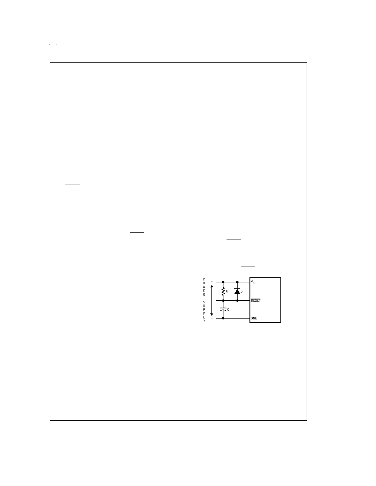
When using external reset, the external RC network shown
in
Figure 6
should be used to ensure that the RESET pin is
held low until the power supply to the chip stabilizes. Under
no circumstances should the RESET pin be allowed to float.
RC 5 x Power Supply Rise Time
DS100044-7
FIGURE 6. Recommended Reset Circuit
www.national.com11
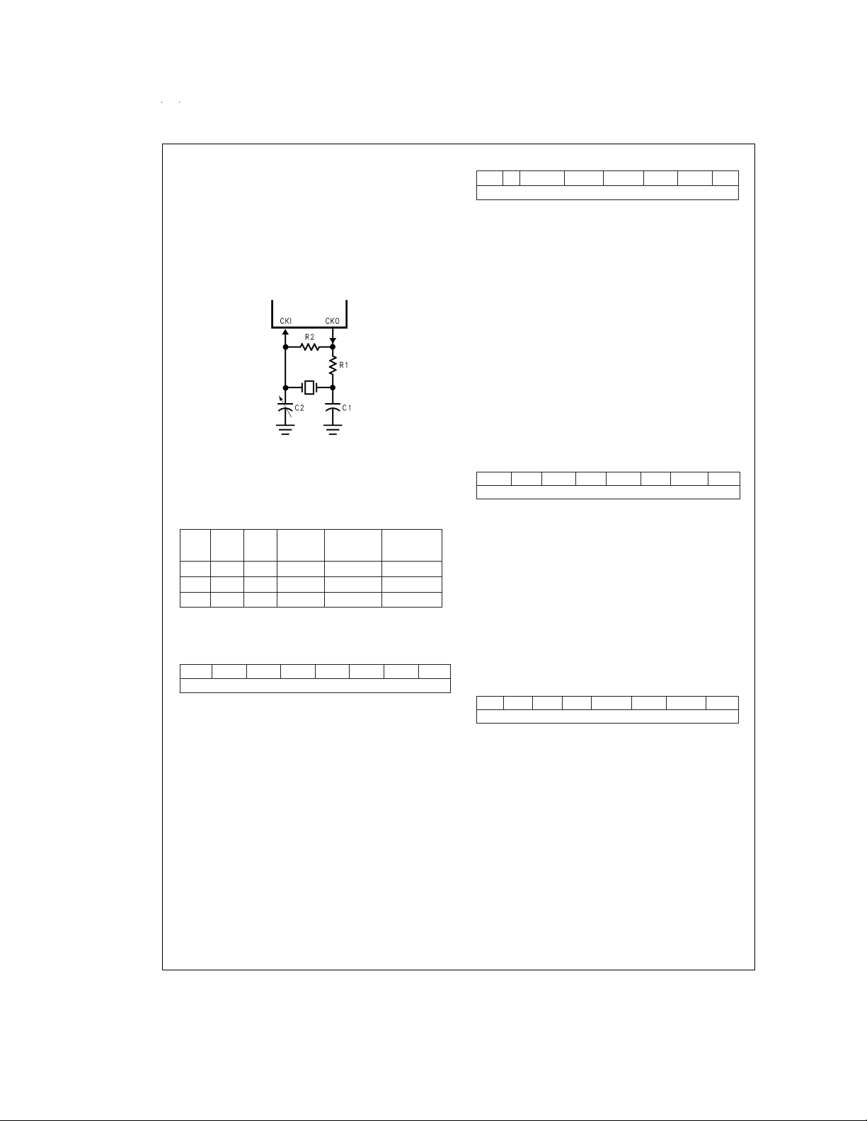
Oscillator Circuits
The chip can be driven by a clock input on the CKI input pin
which can be between DC and 10 MHz. The CKO output
clock is on pin G7. The CKI input frequency is divided by 10
to produce the instruction cycle clock (1/t
Figure 7
shows the Crystal diagram.
).
c
CRYSTAL OSCILLATOR
CKI and CKO can be connected to make a closed loop crystal (or resonator) controlled oscillator.
DS100044-8
FIGURE 7. Crystal Oscillator Diagram
Table 1
shows the component values required for various
standard crystal values.
TABLE 1. Crystal Oscillator Configuration, T
= 25˚C
A
R1 R2 C1 C2 CKI Freq. Conditions
(kΩ)(MΩ) (pF) (pF) (MHz)
0 1 30 30–36 10 V
0 1 30 30–36 4 V
0 1 200 100–150 0.455 V
=5V
CC
=5V
CC
=5V
CC
Control Registers
CNTRL Register (Address X'00EE)
T1C3 T1C2 T1C1 T1C0 MSEL IEDG SL1 SL0
Bit 7 Bit 0
The Timer1 (T1) and MICROWIRE/PLUS control register
contains the following bits:
T1C3 Timer T1 mode control bit
T1C2 Timer T1 mode control bit
T1C1 Timer T1 mode control bit
T1C0 Timer T1 Start/Stop control in timer
modes 1 and 2, T1 Underflow Interrupt
Pending Flag in timer mode 3
MSEL Selects G5 and G4 as MICROWIRE/PLUS
IEDG External interrupt edge polarity select
SL1 & SL0 Select the MICROWIRE/PLUS clock divide
signals SK and SO respectively
(0 = Rising edge, 1 = Falling edge)
by (00 = 2, 01 = 4, 1x = 8)
PSW Register (Address X'00EF)
HC C T1PNDA T1ENA EXPND BUSY EXEN GIE
Bit 7 Bit 0
The PSW register contains the following select bits:
HC Half Carry Flag
C Carry Flag
T1PNDA Timer T1 Interrupt Pending Flag (Autoreload
RA in mode 1, T1 Underflow in Mode 2, T1A
capture edge in mode 3)
T1ENA Timer T1 Interrupt Enable for Timer Underflow
or T1A Input capture edge
EXPND External interrupt pending
BUSY MICROWIRE/PLUS busy shifting flag
EXEN Enable external interrupt
GIE Global interrupt enable (enables interrupts)
The Half-Carry flag is also affectedby all the instructions that
affect the Carry flag. The SC (Set Carry) and R/C (Reset
Carry) instructions will respectively set or clear both thecarry
flags. In addition to the SC and R/C instructions, ADC,
SUBC, RRC and RLC instructions affect the Carry and Half
Carry flags.
ICNTRL Register (Address X'00E8)
Reserved LPEN T0PND T0EN µWPND µWEN T1PNDB T1ENB
Bit 7 Bit 0
The ICNTRL register contains the following bits:
Reserved This bit is reserved and should be zero
LPEN L Port Interrupt Enable (Multi-Input Wakeup/
Interrupt)
T0PND Timer T0 Interrupt pending
T0EN Timer T0 Interrupt Enable (Bit 12 toggle)
µWPND MICROWIRE/PLUS interrupt pending
µWEN Enable MICROWIRE/PLUS interrupt
T1PNDBTimer T1 Interrupt Pending Flag for T1B capture
edge
T1ENB Timer T1 Interrupt Enable for T1B Input capture
edge
T2CNTRL Register (Address X'00C6)
T2C3 T2C2 T2C1 T2C0 T2PNDA T2ENA T2PNDB T2ENB
Bit 7 Bit 0
The T2CNTRL control register contains the following bits:
T2C3 Timer T2 mode control bit
T2C2 Timer T2 mode control bit
T2C1 Timer T2 mode control bit
T2C0 Timer T2 Start/Stop control in timer
modes 1 and 2, T2 Underflow Interrupt Pending Flag in timer mode 3
T2PNDA Timer T2 Interrupt Pending Flag (Autoreload
RA in mode 1, T2 Underflow in mode 2, T2A
capture edge in mode 3)
T2ENA Timer T2 Interrupt Enable for Timer Underflow
or T2A Input capture edge
T2PNDB Timer T2 Interrupt Pending Flag for T2B cap-
ture edge
T2ENB Timer T2 Interrupt Enable for Timer Underflow
or T2B Input capture edge
www.national.com 12
Timers
The device contains a very versatile set of timers (T0, T1 and
T2). All timers and associated autoreload/capture registers
power up containing random data.
TIMER T0 (IDLE TIMER)
The device supports applications that require maintaining
real time and low power with the IDLE mode. This IDLE
mode support is furnished by the IDLE timer T0, which is a
16-bit timer.The Timer T0 runs continuously at the fixed rate
of the instruction cycle clock, t
write to the IDLE Timer T0, which is a count down timer.
The Timer T0 supports the following functions:
Exit out of the Idle Mode (See Idle Mode description)
•
WATCHDOG logic (See WATCHDOG description)
•
Start up delay out of the HALT mode
•
. The user cannot read or
c
Figure 8
is a functional block diagram showing the structure
of the IDLE Timer and its associated interrupt logic.
Bits 11 through 15 of the ITMR register can be selected for
triggering the IDLE Timer interrupt. Each time the selected
bit underflows (every 4k, 8k, 16k, 32k or 64k instruction
cycles), the IDLE Timer interrupt pending bit T0PND is set,
thus generating an interrupt (if enabled), and bit 6 of the Port
G data register is reset, thus causing an exit from the IDLE
mode if the device is in that mode.
In order for an interrupt to be generated, the IDLE Timer interrupt enable bit T0EN must be set, and the GIE (Global Interrupt Enable) bit must also be set. The T0PND flag and
T0EN bit are bits 5 and 4 of the ICNTRL register, respectively.The interrupt can be used for any purpose. Typically, it
is used to perform a task upon exit from the IDLE mode. For
more information on the IDLE mode, refer to the Power Save
Modes section.
FIGURE 8. Functional Block Diagram for Idle Timer T0
The Idle Timer period is selected by bits 0–2 of the ITMR
register Bits 3–7 of the ITMR Register are reserved and
should not be used as software flags.
ITMR Register (Address X’0xCF)
Reserved ITSEL2 ITSEL1 ITSLE0
Bit 7 Bit 0
TABLE 2. Idle Timer Window Length
ITSEL2 ITSEL1 ITSEL0 Idle Timer Period
(Instruction Cycles)
0 0 0 4,096
0 0 1 8,192
0 1 0 16,384
0 1 1 32,768
1 X X 65,536
The ITMR register is cleared on Reset and the Idle Timer period is reset to 4,096 instruction cycles.
Any time the IDLE Timer period is changed there is the possibility of generating a spurious IDLE Timer interrupt by setting the T0PND bit. The user is advised to disable IDLE
Timer interrupts prior to changing the value of the ITSEL bits
of the ITMR Register and then clear the T0PND bit before attempting to synchronize operation to the IDLE Timer.
DS100044-9
TIMER T1 and TIMER T2
The device has a set of three powerful timer/counter blocks,
T1 and T2. The associated features and functioning of a
timer block are described by referring to the timer block Tx.
Since the three timer blocks, T1 and T2 are identical, all
comments are equally applicable to either of the three timer
blocks.
Each timer block consists of a 16-bit timer, Tx, and two supporting 16-bit autoreload/capture registers, RxA and RxB.
Each timer block has two pins associated with it, TxA and
TxB. The pin TxA supports I/O required by the timer block,
while the pin TxB is an input to the timer block. The powerful
and flexible timer block allows the device to easily perform all
timer functions with minimal software overhead. The timer
block has three operating modes: Processor Independent
PWM mode, External Event Counter mode, and Input Capture mode.
The control bits TxC3, TxC2, and TxC1 allow selection of the
different modes of operation.
Mode 1. Processor Independent PWM Mode
As the name suggests, this mode allows the device to generate a PWM signal with very minimal user intervention.
The user only has to define the parameters of the PWM signal (ON time and OFFtime). Once begun, the timer block will
continuously generate the PWM signal completely indepen-
www.national.com13
Timers (Continued)
dent of the microcontroller. The user software services the
timer block only when the PWM parameters require updating.
In this mode the timer Tx counts down at a fixed rate of t
Upon every underflow the timer is alternately reloaded with
the contents of supporting registers, RxA and RxB. The very
first underflow of the timer causes the timer to reload from
the register RxA. Subsequent underflows cause the timer to
be reloaded from the registers alternately beginning with the
register RxB.
The Tx Timer control bits, TxC3, TxC2 and TxC1 set up the
timer for PWM mode operation.
Figure 9
shows a block diagram of the timer in PWM mode.
TxA pin. Underflows from the timer are latched into the TxPNDA pending flag. Setting the TxENA control flag will cause
an interrupt when the timer underflows.
In this mode the input pin TxB can be used as an independent positive edge sensitive interrupt input if the TxENB con-
.
trol flag is set. The occurrence of the positive edge on the
c
TxB input pin is latched to the TxPNDB flag.
Figure 10
shows a block diagram of the timer in External
Event Counter mode.
DS100044-10
FIGURE 9. Timer in PWM Mode
The underflows can be programmed to toggle the TxAoutput
pin. The underflows can also be programmed to generate interrupts.
Underflows from the timer are alternately latched into two
pending flags, TxPNDA and TxPNDB. The user must reset
these pending flags under software control. Two control enable flags, TxENA and TxENB, allow the interrupts from the
timer underflow to be enabled or disabled. Setting the timer
enable flag TxENA will cause an interrupt when a timer underflow causes the RxAregister to bereloaded into the timer.
Setting the timer enable flag TxENB will cause an interrupt
when a timer underflow causes the RxB register to be reloaded into the timer. Resetting the timer enable flags will
disable the associated interrupts.
Either or both of the timer underflow interrupts may be enabled. This gives the user the flexibility of interrupting once
per PWM period on either the rising or falling edge of the
PWM output. Alternatively, the user may choose to interrupt
on both edges of the PWM output.
Mode 2. External Event Counter Mode
This mode is quite similar to the processor independent
PWM mode described above. The main difference is that the
timer,Tx, is clocked by the input signal from the TxA pin. The
Tx timer control bits, TxC3,TxC2 and TxC1 allow the timer to
be clocked either on a positive or negative edge from the
Note: The PWM output is not available in this mode since the TxA pin is
being used as the counter input clock.
DS100044-11
FIGURE 10. Timer in External Event Counter Mode
Mode 3. Input Capture Mode
The device can precisely measure external frequencies or
time external events by placing the timer block, Tx, in the input capture mode.
In this mode, the timer Tx is constantly running at the fixed t
rate. The two registers, RxA and RxB, act as capture registers. Each register acts in conjunction with a pin.The register
RxAacts in conjunction with the TxA pin and the register RxB
acts in conjunction with the TxB pin.
The timer value gets copied over into the register when a
trigger event occurs on its corresponding pin. Control bits,
TxC3, TxC2 and TxC1, allow the trigger events to be specified either as a positive or a negative edge. The trigger condition for each input pin can be specified independently.
The trigger conditions can also be programmed to generate
interrupts. The occurrence of the specified trigger condition
on the TxA and TxB pins will be respectively latched into the
pending flags, TxPNDA and TxPNDB. The control flag
TxENA allows the interrupt on TxA to be either enabled or
disabled. Setting the TxENA flag enables interrupts to be
generated when the selected trigger condition occurs on the
TxA pin. Similarly, the flag TxENB controls the interrupts
from the TxB pin.
Underflows from the timer can also be programmed to generate interrupts. Underflows are latched into the timer TxC0
pending flag (the TxC0 control bit serves as the timer underflow interrupt pending flag in the Input Capture mode). Consequently, the TxC0 control bit should be reset when entering the Input Capture mode. The timer underflow interrupt is
enabled with the TxENA control flag. When a TxA interrupt
occurs in the Input Capture mode, the user must check both
whether a TxA input capture or a timer underflow (or both)
caused the interrupt.
Figure 11
shows a block diagram of the timer in Input Cap-
ture mode.
c
www.national.com 14
Timers (Continued)
FIGURE 11. Timer in Input Capture Mode
TIMER CONTROL FLAGS
The control bits and their functions are summarized below.
TxC3 Timer mode control
TxC2 Timer mode control
TxC1 Timer mode control
TxC0 TimerStart/Stop control in Modes 1 and 2 (Pro-
cessor Independent PWM and External Event
Counter), where 1 = Start, 0 = Stop
Timer Underflow Interrupt Pending Flag in
Mode 3 (Input Capture)
The timer mode control bits (TxC3, TxC2 and TxC1) are detailed below:
TxPNDA Timer Interrupt Pending Flag
TxENA Timer Interrupt Enable Flag
TxPNDB Timer Interrupt Pending Flag
TxENB Timer Interrupt Enable Flag
DS100044-12
1 = Timer Interrupt Enabled
0 = Timer Interrupt Disabled
1 = Timer Interrupt Enabled
0 = Timer Interrupt Disabled
Mode TxC3 TxC2 TxC1 Description
1 0 1 PWM: TxA Toggle Autoreload RA Autoreload RB t
1
1 0 0 PWM: No TxA
Toggle
0 0 0 External Event
2
0 0 1 External Event
Counter
Counter
0 1 0 Captures: Pos. TxA Edge Pos. TxB Edge t
TxA Pos. Edge or Timer
TxB Pos. Edge Underflow
1 1 0 Captures: Pos. TxA Neg. TxB t
TxA Pos. Edge Edge or Timer Edge
3
0 1 1 Captures: Neg. TxA Neg. TxB t
TxB Neg. Edge Underflow
TxA Neg. Edge Edge or Timer Edge
TxB Neg. Edge Underflow
1 1 1 Captures: Neg. TxA Neg. TxB t
TxA Neg. Edge Edge or Timer Edge
TxB Neg. Edge Underflow
Interrupt A
Source
Interrupt B
Source
Autoreload RA Autoreload RB
Timer
Pos. TxB Edge Pos. TxA
Underflow
Timer
Pos. TxB Edge Pos. TxA
Underflow
Timer
Counts On
C
t
C
Edge
Edge
C
C
C
C
www.national.com15
Power Save Modes
The device offer the user two power save modesof operation: HALT and IDLE. In the HALT mode, all microcontroller activities are stopped. In the IDLE mode, the on-board
oscillator circuitry and timer T0 are active but all other microcontroller activities are stopped. In either mode, all onboard RAM, registers, I/O states, and timers (with the exception of T0) are unaltered.
HALT MODE
The device is placed in the HALT mode by writing a ’’1” to
the HALT flag (G7 data bit). All microcontroller activities,
including the clock, and timers, are stopped. In the HALT
mode, the power requirements of the device are minimal
and the applied voltage (V
(Vr = 2.0V) without altering the state of the machine.
) may be decreased to Vr
CC
In order to reduce the device overall current consumption
in HALT/IDLEmode a two step power save mechanism is
implemented on the device:
Step 1: Disable main receive comparator. This is done
by resetting both the TxEN0 and TxEN1 bits in
the CBUS register. Note: These bits should always be reset before entering HALT/IDLEmode
to allow proper resynchronization to the CAN
bus after exiting HALT/IDLE mode.
Step 2: Disable the CAN wake-up comparators, this is
done by resetting bit 7 in the port-m wakeup enable register (MWKEN) a transition on the CAN
bus will then not wake the device up.
Note: If both the main receive comparator and the wake-up comparator
are disabled the on chip CAN voltage reference is also disabled.
The CAN-V
output is then High-Z
REF
CAN HALT/IDLE mode:
The following table shows the two CAN power save modes and the active CAN transceiver blocks:
Step 1 Step 2 Main-Comp Wake-Up-Comp CAN-V
0 0 on on on V
0 1 on off on V
1 0 off on on V
1 1 off off off High-Z
The device supports two different ways of exiting the HALT
mode. The first method of exiting the HALTmode is with the
Multi-Input Wakeup feature on the L & M port. The second
method of exiting the HALT mode is by pulling the RESET
pin low.
Since a crystal or ceramic resonator may be selected as the
oscillator, the Wakeup signal is not allowed to start the chip
running immediately since crystal oscillators and ceramic
resonators have a delayed start up time to reach full amplitude and frequency stability. The IDLE timer is used to generate a fixed delay to ensure that the oscillator has indeed
stabilized before allowing instruction execution. In this case,
upon detecting a valid Wakeup signal, only the oscillator circuitry is enabled. The IDLE timer is loaded with a value of
256 and is clocked with the t
clock is derived by dividingthe oscillator clock down by a fac-
instruction cycle clock. The t
c
tor of 10. The Schmitt trigger following the CKI inverter on
the chip ensures that theIDLE timer is clocked only when the
oscillator has a sufficiently large amplitude to meet the
Schmitt trigger specifications. This Schmitt trigger is not part
of the oscillator closed loop. The start-up time-out from the
IDLE timer enables the clock signals to be routed to the rest
of the chip.
The device has two mask options associated with the HALT
mode. The first mask option enables the HALTmode feature,
As with the HALT mode, the device can be returned to normal operation with a reset, or with a Multi-Input Wakeup from
the Port L or CAN Interface. Alternately, the microcontroller
resumes normal operation from the IDLE mode when the
thirteenth bit (representing 4.096 ms at internal clock frequency of 1 MHz, t
This toggle condition of the thirteenth bit of the IDLE Timer
T0 is latched into the T0PND pending flag.
The user has the option of being interrupted with a transition
on the thirteenth bit of the IDLE Timer T0. The interrupt can
be enabled or disabled via the T0EN control bit. Setting the
T0EN flag enables the interrupt and vice versa.
The user can enter the IDLE mode with the Timer T0 interrupt enabled. In this case, when the T0PND bit gets set, the
c
device will first execute the TimerT0 interrupt service routine
and then return to the instruciton following the “Enter Idle
Mode” instruction.
Alternatively, the user can enter the IDLE mode with the
IDLE TimerT0 interrupt disabled. In this case, the device will
resume normal operation with the instruction immediately
following the “Enter IDLE Mode” instruction.
Note: It is necessary to program two NOP instructions following both the set
HALT mode and set IDLE mode instructions. These NOP instructions
are necessary to allow clock resynchronization following the HALT or
IDLE modes.
while the second mask option disables the HALTmode. With
the HALT mode enable mask option, the device will enter
and exit the HALTmode as described above. With the HALT
disable mask option, the device cannot be placed in the
HALTmode (writing a “1” to the HALT flag will have to effect).
IDLE MODE
The device is placed in the IDLE mode by writing a “1” to the
IDLE flag (G6 data bit). In this mode, all activity, except the
associated on-board oscillator circuitry, ad the IDLE Timer
T0, is stopped. The power supply requirements of the microcontroller in this mode of operation are typically around 30
%
of normal power requirement of the microcontroller.
www.national.com 16
Multi-Input Wakeup
The Multi-Input Wakeup feature is used to return (wakeup)
the device from either the HALT or IDLE modes. Alternately,
the Multi-Input Wakeup/Interrupt feature may also be used to
generate up to 7 edge selectable external interrupts.
Note: The following description is for both the Port L and the M port. When
the document refers to the registers WKEGD, WKEN or WKPND, the
user will have to put either M (for M port) or L (for port) in front of the
register, i.e., LWKEN (Port L WKEN), MWKEN (Port M WKEN).
Figures 12, 13
microcontroller.The Multi-Input Wakeupfeature utilizes the L
Port. The user selects which particular Port L bit (or combi-
V
REF
= 1 µs) of the IDLE Timer toggles.
c
REF
Pin
/2
CC
/2
CC
/2
CC
shows the Multi-Input Wakeup logic for the

Multi-Input Wakeup (Continued)
nation of Port L bits) will cause the device to exit the HALTor
IDLE modes. The selection is done through the Reg: WKEN.
The Reg: WKEN is an 8-bit read/write register, which contains a control bit for every Port L bit. Setting a particular
WKEN bit enables a Wakeup from the associated Port L pin.
The user can select whether the trigger condition on the selected Port L pin is going to be either a positive edge (low to
high transition) or a negative edge (high to low transition).
This selection is made via the Reg: WKEDG, which is an
8-bit control register with a bit assigned to each Port L pin.
Setting the control bit will select the trigger condition to be a
negative edge on that particular Port L pin. Resetting the bit
selects the trigger condition to be a positive edge. Changing
an edge select entails several steps in order to avoid a
pseudo Wakeup condition as a result of the edge change.
First, the associated WKEN bit should be reset, followed by
the edge select change in WKEDG. Next, the associated
WKPND bit should be cleared, followed by the associated
WKEN bit being re-enabled.
An example may serve to clarify this procedure. Suppose we
wish to change the edge select from positive (low going high)
to negative (high going low) for Port L bit 5, where bit 5 has
previously been enabled for an input interrupt. The program
would be as follows:
RBIT 5, WKEN ;Disable MIWU
SBIT 5, WKEDG ;Change edge polarity
RBIT 5, WKPND ;Reset pending flag
SBIT 5, WKEN ;Enable MIWU
If the Port L bits have been used as outputs and then
changed to inputs with Multi-Input Wakeup/Interrupt, a safety
procedure should also be followed to avoid inherited pseudo
wakeup conditions. After the selected Port L bits have been
changed from output to input but before the associated
WKEN bits are enabled, the associated edge select bits in
WKEDG should be set or reset for the desired edge selects,
followed by the assoicated WKPND bits being cleared.
FIGURE 12. Port M Multi-Input Wake-up Logic
This same procedure should be used following reset, since
the Port L inputs are left floating as a result of reset. The occurrence of the selected trigger condition for Multi-Input
Wakeup is latched to a pending register called WKPND. The
respective bits of the WKPND register will be set on the occurrence of the selected trigger edge on the corresponding
Port L and Port M pin. The user has the responsibility of
clearing these pending flags. Since WKPND is a pending
register for the occurrence of selected wakeup conditions,
the device will not enter the HALT mode if any wakeup bit is
both enabled and pending. Consequently, the user has the
responsibility of clearing the pending flags before attempting
to enter the HALT mode.
DS100044-13
The WKEN, WKPND and WKEDG are all read/write registers, and are cleared at reset.
PORT L INTERRUPTS
Port Lprovides the user with additional eight fully selectable,
edge sensitive interrupts which are all vectored into the
same service subroutine.
The interrupt from Port L shares logic with the wake up circuitry.The register WKEN allows interrupts from Port L to be
individually enabled or disabled. The register WKEDG specifies the trigger condition to be either a positive or a negative
edge. Finally, the register WKPND latches in the pending
trigger conditions.
www.national.com17
Multi-Input Wakeup (Continued)
The GIE (global interrupt enable) bit enables the interrupt
function. A control flag, LPEN, functions as a global interrupt
enable for Port L interrupts. Setting the LPEN flag will enable
interrupts and vice versa. A separate global pending flag is
not needed since the register WKPND is adequate.
Since Port L is also used for waking the device out of the
HALTor IDLE modes, the user can elect to exit the HALT or
IDLE modes either with or without the interrupt enabled. If he
elects to disable the interrupt, then the device will restart execution from the instruction immediately following the instruction that placed the microcontroller in the HALT or IDLE
modes. In the other case, the device will first execute the interrupt service routine and then revert to normal operation.
The Wakeup signal will not start the chip running immediately since crystal oscillators or ceramic resonators have afi-
nite start up time. The IDLE Timer (T0) generates a fixed delay to ensure that the oscillator has indeed stabilized before
allowing the device to execute instructions. In this case,
upon detecting a valid Wakeup signal, only the oscillator circuitry and the IDLE Timer T0 are enabled. The IDLE Timer is
loaded with a value of 256 and is clocked from the t
tion cycle clock. The t
oscillator clock by a factor of 10. A Schmitt trigger following
clock is derived by dividing down the
c
instruc-
c
the CKI on-chip inverter ensures that the IDLE timer is
clocked only when the oscillator has a sufficiently large amplitude to meet the Schmitt trigger specifications. This
Schmitt trigger is not part of the oscillator closed loop. The
start-up time-out from the IDLE timer enables the clock signals to be routed to the rest of the chip.
FIGURE 13. Port L Multi-Input Wake-Up Logic
PORT M INTERRUPTS
Port M provides the user with seven fully selectable, edge
sensitive interrupts which are all vectored into the same service subroutine.
The interrupt from Port M shares logic with the wake up circuitry.The MWKEN register allows interrupts from Port M to
be individually enabled or disabled. The MWKEDG register
specifies the trigger condition to be either a positive or a
negative edge. The MWKPND register latches in the pending trigger conditions.
The LPEN control flag in the ICNTRL register functions as a
global interrupt enable for Port M interrupts. Setting the
LPEN flag enables interrupts. Note that the GIE bit in the
PSW register must also be set to enable these Port L interrupts.A global pending flag is not needed since each pin has
a corresponding pending flag in the MWKPND register.
Since Port M is also used for exiting the device from the
HALT or IDLE mode, the user can elect to exit the HALT or
IDLE mode either with or without the interrupt enabled. If the
user elects to disable the interrupt, then the device restarts
execution from the point at which it was stopped (first in-
www.national.com 18
DS100044-14
struction cycle of the instruction following the enter HALT or
IDLE mode instruction). In the other case, the devicefinishes
the instruction which was being executed when the part was
stopped (the NOP(Note *NO TARGET FOR FNXref
NS9529*) instruction following the enter HALT or IDLE mode
instruction), and then branches to the interrupt service routine. The device then reverts to normal operation.
Note 16: The user must place two NOPs after an enter HALT or IDLE mode
instruction.
To prevent erroneous clearing of the SPI receive FIFO when
entering HALT/IDLE mode, the user needs to enable the
MIWU on port M3. (SS) by setting bit 3 in the MWKEN register.
CAN RECEIVE WAKEUP
The CAN Receive Wakeup source can be enabled or disabled. There is no specific enable bit for the CAN Wakeup
feature. Although the wakeup feature on pins L0..17 and
M0..M7 can be programmed to generate an interrupt (Port L
or Port M interrupt), no interrupt is generated upon a CAN re-

Multi-Input Wakeup (Continued)
ceive wakeup condition. The CAN block has it’s own, dedicated receiver interrupt upon receive buffer full (see CAN
Section).
CAN Wake-Up:
The CAN interface can be programmed to wake the device
from HALT/IDLE mode. This is done by setting bit 7 in the
Port M wake-up enable register (MWKEN). A transition on
the bus will cause the bit 7 of the Port M wake-up pending
(MWKPND) to be set and thereby waking up the device. The
frame on the CAN bus will be lost. The MWEDG (m port
wake-up edge) register bit 7 can be programmed high or low
(high will wake-up on the first falling edge on Rx0).
Resetting bit 7 in the MWKEN will disable the CAN wake-up.
The following sequence should be executed before entering
HALT/IDLE mode:
RBIT 7, MWKPND ;clear CAN wake-up pending
LD A, CBUS
AND A, #0CF ;resetTxEN0 and TxEN1
X A, CBUS ;disable main receive
;comparator
After the device woke-up the CBUS bits TxEN0 and/or
TxEN1 need be set to allow synchronization on the bus and
to enable transmission/reception of CAN frames.
CAN Block Description *
This device contains a CAN serial bus interface as described
in the CAN Specification Rev. 2.0 part B.
*Patents Pending.
CAN Interface Block
This device supports applications which require a low speed
CAN interface. It is designed to be programmed with two
transmit and two receive registers. The user’s program may
check the status bytes in order to get information of the bus
state and the received or transmitted messages. The device
has the capability to generate an interrupt as soon as one
byte has been transmitted or received. Care must be taken if
more than two bytes in a message frame are to be
transmitted/received. In this case the user’s program must
poll the transmit buffer empty (TBE)/receive buffer full (RBF)
bits or enable their respective interrupts and perform a data
exchange between the user data and the Tx/Rx registers.
Fully automatic transmission on error is supported for messages not longer than two bytes. Messages which are longer
than two bytes have to be processed by software.
The interface is compatible with CAN Specification 2.0 part
B, without the capability to receive/transmit extended
frames. Extended frames on the bus are checked and acknowledged according to the CAN specification.
The maximum bus speed achievable with the CAN interface
is a function of crystal frequency, message length and software overhead.The device can support a bus speed of up to
1 Mbit/s with a 10 MHz oscillator and 2 byte messages. The
1 Mbit/s bus speed refers to the rate at which protocol and
data bits are transferred on the bus. Longer messages require slower bus speeds due to the time required for software intervention between data bytes. The device will support a maximum of 125k bit/s with eight byte messages and
a 10 MHz oscillator.
www.national.com19
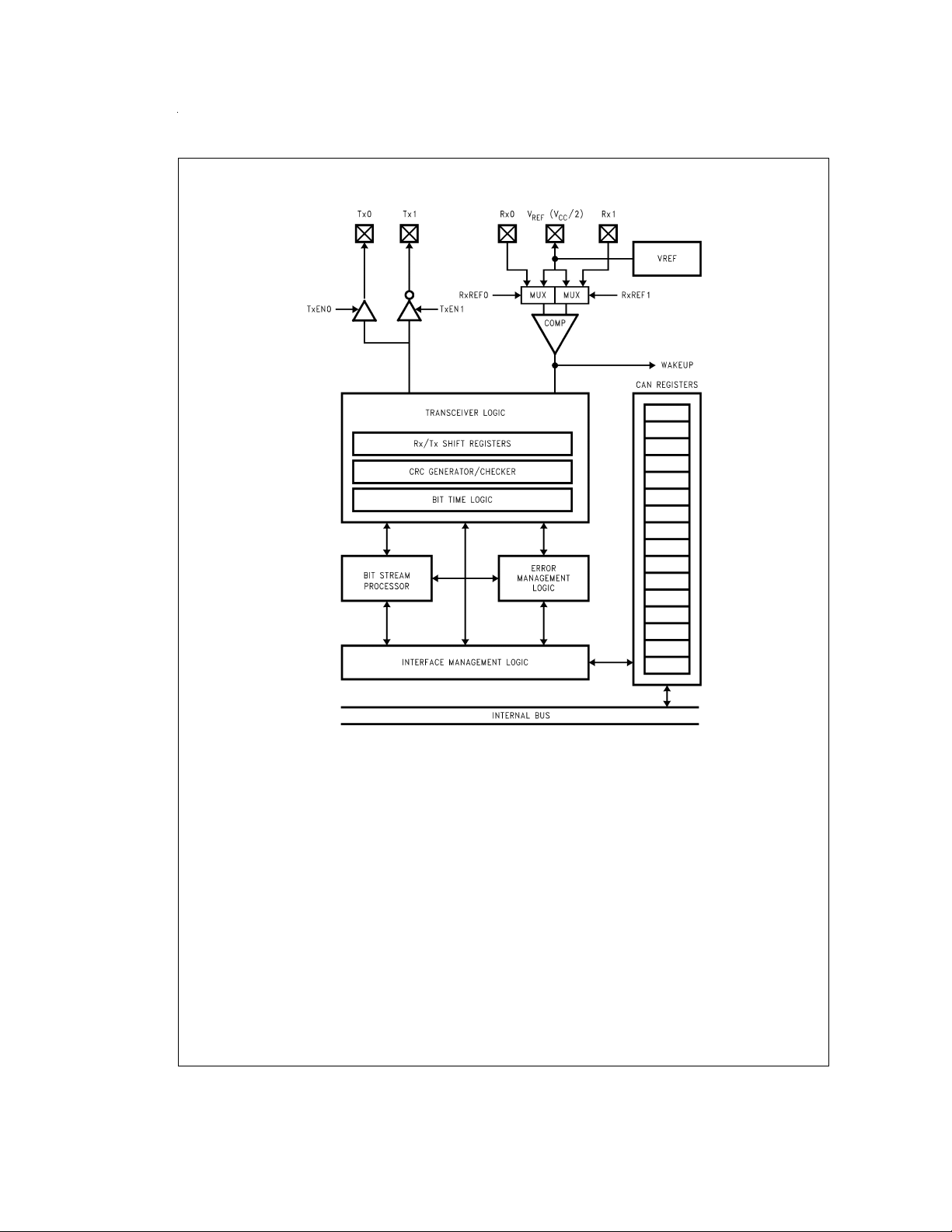
CAN Interface Block (Continued)
FIGURE 14. CAN Interface Block Diagram
Functional Block Description of
the CAN Interface
Interface Management Logic (IML)
The IML executes the CPU’s transmission and reception
commands and controls the data transfer between CPU,
Rx/Tx and CAN registers. It provides the CAN Interface with
Rx/Tx data from the memory mapped Register Block. It also
sets and resets the CAN status information and generates
interrupts to the CPU.
Bit Stream Processor (BSP)
The BSPis a sequencer controlling the data stream between
The Interface Management Logic (parallel data) and the bus
line (serial data). It controls the transceive logic with regard
to reception and arbitration, and creates error signals according to the bus specification.
www.national.com 20
DS100044-16
Transceive Logic (TCL)
The TCL is a state machine which incorporates the bit stuff
logic and controls the output drivers, CRC logic and the
Rx/Tx shift registers. It also controls the synchronization to
the bus with the CAN clock signal generated by the BTL.
Error Management Logic (EML)
The EML is responsible for the fault confinement of the CAN
protocol. It is also responsible for changing the error
counters, setting the appropriate error flag bits and interrupts
and changing the error status (passive, active and bus off).
Cyclic Redundancy Check (CRC)
Generator and Register
The CRC Generator consists of a 15-bit shift register and the
logic required to generate the checksum of the destuffed bitstream. It informs the EML about the result of a receiver
checksum.
The checksum is generated by the polynomial:
15
14
10
8
7
4
χ
+
χ
+
χ
+
χ
+
χ
3
+
χ
+
χ
−1
Functional Block Description of
the CAN Interface
Receive/Transmit (Rx/Tx) Registers
The Rx/Tx registers are 8-bit shift registers controlled by the
TCL and the BSP. They are loaded or read by the Interface
Management Logic, which holds the data to be transmitted
or the data that was received.
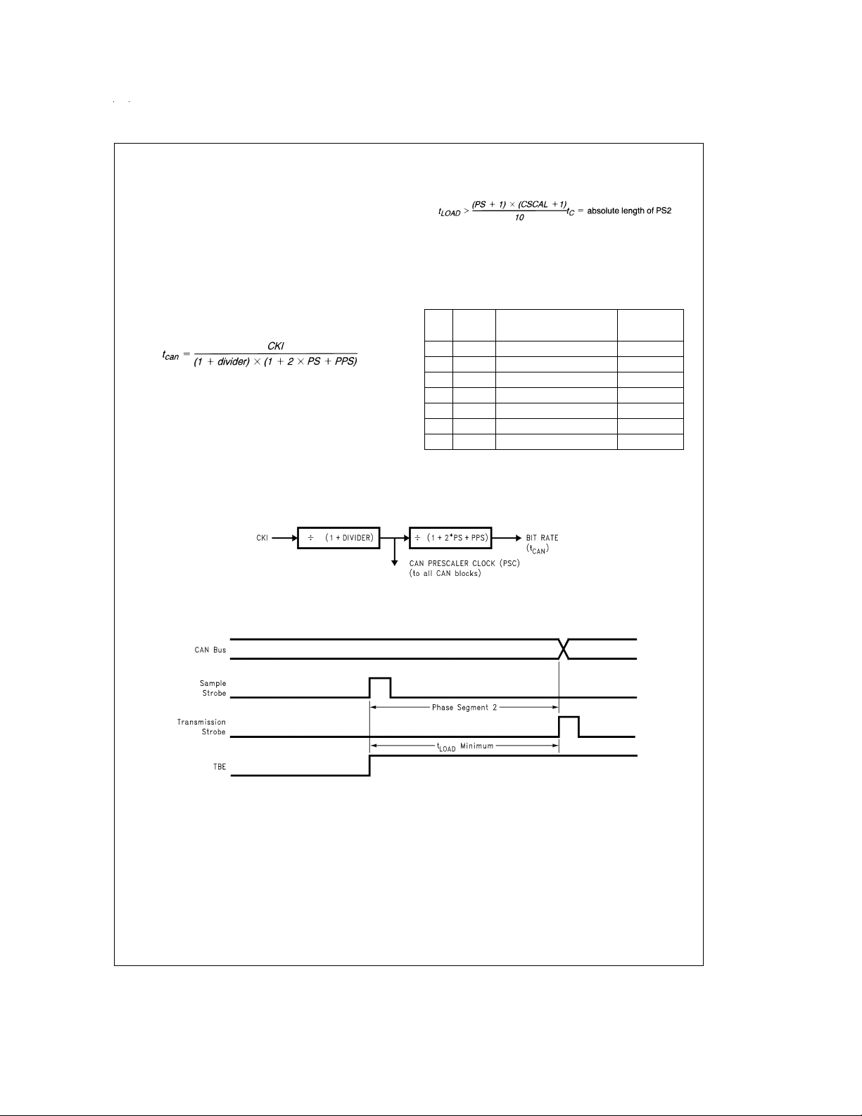
Bit Time Logic (BTL)
The bit time logic divider divides the CKI input clock by the
value defined in the CAN prescaler (CSCAL) and bus timing
register (CTIM). The resultig bit time (tcan) can be computed
by the formula:
Where
divider
programmable value of phase segment 1 and 2 (1..8) and
PPS
(1..8) (located in CTIM).
Bus Timing Considerations
The internal architecture of the CAN interface has been optimized to allow fast software response times within messages of more than two data bytes. The TBE (Transmit
Buffer Empty) bit is set on the last bit of odd data bytes when
CAN internal sample points are high.
is the value of the clock prescaler,PSis the
the programmed value of the propagation segment
(Continued)
It is the user’s responsibility to ensure that the time between
setting TBE and a reload of TxD2 is longer than the length of
phase segment 2 as indicated in the following equation:
Table 3
shows examples of the minimum required t
different CSCAL settings based on a clock frequency of
LOAD
for
10 MHz. Lower clock speeds require recalculation of the
CAN bit rate and the mimimum t
TABLE 3. CAN Timing (CKI = 10 MHz, t
PS CSCAL CAN Bit Rate (kbit/s)
LOAD
.
= 1 µs)
c
Minimum
t
(µs)
LOAD
4 3 250 2.0
4 9 100 5.0
4 15 62 8.0
4 24 40 12.5
439 25 20
499 10 50
4 199 5 100
FIGURE 15. Bit Rate Generation
Figure 16
illustrates the minimum time required for t
LOAD
.
FIGURE 16. TBE Timing
In the case of an interrupt driven CAN interface, the calculation of the actual t
time would be done as follows:
LOAD
INT: ;Interrupt latency = 7tc=7µs
PUSH A ; 3tc=3µs
LD A,B;2tc=2µs
PUSH A ; 3tc=3µs
VIS ;5tc=5µs
CANTX: ;20tc = µs to this point
•
;additional time for instructions
;which check
•
;status prior to reloading the
;transmit data
DS100044-17
DS100044-18
•
;registers with subsequent data
;bytes.
LD TXD2,DATA
•
•
•
Interrupt driven programs use more time than programs
which poll the TBE flag, however programs which operate at
lower baud rates (which are more likely to be sensitive to this
issue) have more time for interrupt response.
www.national.com21
Functional Block Description of
the CAN Interface
Output Drivers/Input Comparators
The output drivers/input comparators are the physical interface to the bus. Control bits are provided to TRI-STATE the
output drivers.
A dominant bit on the bus is represented as a “0” in the data
registers and a recessive bit on the bus is represented as a
“1” in the data registers.
TABLE 4. Bus Level Definition
Bus Level Pin Tx0 Pin Tx1 Data
“dominant” drive low dirve high 0
“recessive” TRI-STATE TRI-STATE 1
Register Block
The register block consists of fifteen 8-bit registers which are
described in more detail in the following paragraphs.
Note: The contents of the receiver related registers RxD1, RxD2, RDLC,
RIDH and RTSTAT are only changed if a received frame passes the
acceptance filter or the Receive Identifier Acceptance Filter bit (RIAF)
is set to accept all received messages.
TRANSMIT DATA REGISTER 1 (TXD1) (Address
X’00A0)
The Transmit Data Register 1 contains the first data byte to
be transmitted within a frame and then the successive odd
byte numbers (i.e., bytes number 1,3,..,7).
TRANSMIT DATA REGISTER 2 (TXD2)(Address X’00A1)
The Transit Data Register 2 contains the second data byte to
be transmitted within a frame and then the successive even
byte numbers (i.e., bytes number 2,4,..,8).
TRANSMIT DATA LENGTH CODE AND IDENTIFIER
LOW REGISTER (TDLC) (Address X’00A2)
TID3 TID2 TID1 TID0 TDLC3 TDLC2 TDLC1 TDLC0
Bit 7 Bit 0
This register is read/write.
TID3..TIDO Transmit Identifier Bits 3..0 (lower 4 bits)
The transmit identifier is composed of eleven bits in total, bits
3 to 0 of the TID are stored in bits 7 to 4 of this register.
TDLC3..TDLC0 Transmit Data Length Code
These bits determine the number of data bytes to be trans-
mitted within a frame. The CAN specification allows a maximum of eight data bytes in any message.
TRANSMIT IDENTIFIER HIGH (TID) (Address X’00A3)
TRTR TID10 TID9 TID8 TID7 TID6 TID5 TID4
Bit 7 Bit 0
This register is read/write.
TRTR Transmit Remote Frame Request
This bit is set if the frame to be transmitted is a remote frame
request.
TID10..TID4 Transmit Identifier Bits 10 .. 4 (higher 7 bits)
Bits TID10..TID4 are the upper 7 bits of the 11 bit transmit
identifier.
(Continued)
(GND) (V
)
CC
RECEIVER DATA REGISTER 1 (RXD1) (Address
X’00A4)
The Receive Data Register 1 (RXD1) contains the first data
byte received in a frame and then successive odd byte numbers (i.e., bytes 1, 3,..7). This register is read-only.
RECEIVE DATA REGISTER 2 (RXD2) (Address X’00A5)
The Receive Data Register 2 (RXD2) contains the second
data byte received in a frame and then successive even byte
numbers (i.e., bytes 2,4,..,8). This register is read-only.
REGISTER DATA LENGTH CODE AND IDENTIFIERLOW
REGISTER (RIDL) (Address X’00A6)
RID3 RID2 RID1 RID0 RDLC3 RDLC2 RDLC1 RDLC0
Bit 7 Bit 0
This register is read only.
RID3..RID0 Receive Identifier bits (lower four bits)
The RID3..RID0 bits are the lower four bits of the eleven bit
long Receive Identifier. Any received message that matches
the upper 7 bits of the Receive Identifier (RID10..RID4) is accepted if the Receive IdentifierAcceptance Filter (RIAF) bit is
set to zero.
RDLC3..RDLC0 Receive Data Length Code bits
The RDLC3..RDLC0 bits determine the number of data
bytes within a received frame.
RECEIVE IDENTIFIER HIGH (RID) (Address X’00A7)
Reserved RID10 RID9 RID8 RID7 RID6 RID5 RID4
Bit 7 Bit 0
This register is read/write.
Bit 7 is reserved and should be zero.
RID10..RID4 Receive Identifier bits (upper bits)
The RID10...RID4 bits are the upper 7 bits of the eleven bit
long Receive Identifier. If the Receive Identifier Acceptance
Filter (RIAF) bit (see CBUS register) is set to zero, bits 4 to
10 of the received identifier are compared with the mask bits
of RID4..RID10. If the corresponding bits match, the message is accepted. If the RIAF bit is set to a one, the filter
function is disabled and all messages, independent of identifier, will be accepted.
CAN PRESCALER REGISTER (CSCAL) (Address
X’00A8)
CKS7 CKS6 CKS5 CKS4 CKS3 CKS2 CKS1 CKS0
Bit 7 Bit0
This register is read/write.
CKS7..0 Prescaler divider select.
The resulting clock value is the CAN Prescaler clock.
CAN BUS TIMING REGISTER (CTIM) (00A9)
PPS2 PPS1 PPS0 PS2 PS1 PS0 Reserved Reserved
Bit 7 Bit 0
This register is read/write.
PPS2..PPS0 Propagation Segment, bits 2..0
The PPS2..PPS0 bits determine the length of the propaga-
tion delay in Prescaler clock cycles (PSC) per bit time. (For
a more detailed discussion of propagation delay and phase
segments, see SYNCHRONIZATION.)
PS2..PS0 Phase Segment 1, bits 2..0
www.national.com 22
 Loading...