

查询COP87L84FH供应商
COP87L88FH
8-Bit CMOS OTP Microcontrollers with 16k Memory,
Comparators, USART and Hardware Multiply/Divide
General Description
The COP87L88FH OTP (One Time Programmable) microcontrollers are highly integrated COP8
vices with 16k memory and advanced features including
Analog comparators, and Hardware Multiply/Divide. These
multi-chip CMOS devices are suited for applications requiring a full featured controller with comparators, a full-duplex
USART, and hardware multiply/divide functions, and as
pre-production devices for a masked ROM design. Lower
cost pin and software compatible 12k ROM versions are
available (COP888FH),aswell as a range of COP8 software
and hardware development tools.
™
Feature core de-
September 1999
Family features include an 8-bit memory mapped architecture, 10 MHz CKI (-XE=crystal oscillator; -TE=external
clock) with 1µs instruction cycle, hardware multiply/divide
functions, three multi-function 16-bit timer/counters with
PWM, full duplex USART, MICROWIRE/PLUS
comparators, two power saving HALT/IDLE modes, MIWU,
idle timer, WATCHDOG
2.7V to 5.5V operation, and 28/40/44 pin packages.
Devices included in this data sheet are:
™
and clock monitor logic, low EMI
™
, two Analog
COP87L88FH 8-Bit CMOS OTP Microcontrollers with 16k Memory, Comparators, USART and
Hardware Multiply/Divide
Device Memory (bytes) RAM (bytes) I/O Pins Packages Temperature
COP87L84FH 16k OTP EPROM 512 24 28 DIP/SOIC -40 to +85˚C
COP87L88FH 16k OTP EPROM 512 36/40 40 DIP, 44 PLCC -40 to +85˚C
Key Features
n Hardware Multiply/Divide Functions
n Full duplex USART
n Three 16-bit timers, each with two 16-bit registers
supporting:
— Processor Independent PWM mode
— External Event counter mode
— Input Capture mode
n 16 kbytes on-board EPROM with security features
n 512 bytes on-board RAM
Additional Peripheral Features
n Idle Timer
n Multi-Input Wakeup (MIWU) with optional interrupts (8)
n Two analog comparators
n WATCHDOG and Clock Monitor logic
n MICROWIRE/PLUS serial I/O
I/O Features
n Software selectable I/O options ( TRI-STATE®,
Push-Pull, Weak Pull-Up, and High Impedance)
n Schmitt trigger inputs on ports G and L
n Packages:
— 40 DIP with 36 I/O pins
— 44 PLCC with 40 I/O pins
— 28 DIP/SO with 24 I/O pins
CPU/Instruction Set Features
n 1 µs instruction cycle time
n Fourteen multi-source vectored interrupts servicing
— External Interrupt
— Idle Timer T0
— Three Timers (Each with 2 Interrupts)
— MICROWIRE/PLUS
— Multi-Input Wake Up
— Software Trap
— USART (2)
— Default VIS (default interrupt)
n Versatile and easy to use instruction set
n 8-bit Stack Pointer (SP)— stack in RAM
n Two 8-bit Register Indirect Data Memory Pointers
(B and X)
Fully Static CMOS
n Two power saving modes: HALT and IDLE
n Single supply operation: 2.7V–5.5V
n Temperature ranges: −40˚C to +85˚C
Development Support
n Emulation device for COP888FH
n Real time emulation and full program debug offered by
MetaLink Development System
COP8™is a trademark of National Semiconductor Corporation.
™
MICROWIRE
MICROWIRE/PLUS
TRI-STATE
WATCHDOG
iceMASTER
© 1999 National Semiconductor Corporation DS101135 www.national.com
is a trademark of National Semiconductor Corporation.
™
is a trademark of National Semiconductor Corporation.
®
is a registered trademark of National Semiconductor Corporation.
™
is a trademark of National Semiconductor Corporation.
™
is a trademark of MetaLink Corporation.
Block Diagram
DS101135-1
FIGURE 1. COP87L88FH Block Diagram
www.national.com 2
Connection Diagrams
Plastic Chip Carrier
DS101135-2
Top View
Order Number COP87L88FHV-XE/TE
See NS Plastic Chip Package Number V44A
Dual-In-Line Package
DS101135-3
Top View Order
Number COP87L88FHN-XE/TE
See NS Molded Package Number N40A
Dual-In-Line Package
Note: -X Crystal Oscillator
-T External Clock
-E Halt Mode Enable
DS101135-4
Order Number COP87L84FHM-XE/TE, or COP87L84FHN-XE/TE
See NS Molded Package Number M28B or N28B
FIGURE 2. Connection Diagrams
www.national.com3

Connection Diagrams (Continued)
Pinouts for 28-, 40- and 44-Pin Packages
Port Type Alt. Fun Alt. Fun
L0 I/O MIWU 11 17 17
L1 I/O MIWU CKX 12 18 18
L2 I/O MIWU TDX 13 19 19
L3 I/O MIWU RDX 14 20 20
L4 I/O MIWU T2A 15 21 25
L5 I/O MIWU T2B 16 22 26
L6 I/O MIWU T3A 17 23 27
L7 I/O MIWU T3B 18 24 28
G0 I/O INT 25 35 39
G1 WDOUT 26 36 40
G2 I/O T1B 27 37 41
G3 I/O T1A 28 38 42
G4 I/O SO 1 3 3
G5 I/O SK 2 4 4
G6ISI 355
G7 I/CKO HALT Restart 4 6 6
D0O 192529
D1O 202630
D2O 212731
D3O 222832
D4 O 29 33
D5 O 30 34
D6 O 31 35
D7 O 32 36
I0I 799
I1 I COMP1IN− 8 10 10
I2 I COMP1IN+ 9 11 11
I3 I COMP1OUT 10 12 12
I4 I COMP2IN− 13 13
I5 I COMP2IN+ 14 14
I6 I COMP2OUT 15 15
I7 I 16 16
C0 I/O 39 43
C1 I/O 40 44
C2 I/O 1 1
C3 I/O 2 2
C4 I/O 21
C5 I/O 22
C6 I/O 23
C7 I/O 24
V
CC
GND 23 33 37
CKI 5 7 7
RESET
28-Pin 40-Pin 44-Pin
Pack. Pack. Pack.
688
24 34 38
www.national.com 4
Absolute Maximum Ratings (Note 1)
If Military/Aerospace specified devices are required,
please contact the National Semiconductor Sales Office/
Distributors for availability and specifications.
Supply Voltage (V
Voltage at Any Pin −0.3V to V
)7V
CC
CC
+ 0.3V
Total Current into V
Pin (Source) 100 mA
CC
Total Current out of GND Pin (Sink) 110 mA
Storage Temperature Range −65˚C to +140˚C
Note 1: Absolute maximum ratings indicate limits beyond which damage to
the device may occur. DC and AC electrical specifications are not ensured
when operating the device at absolute maximum ratings.
DC Electrical Characteristics
−40˚C ≤ TA≤ +85˚C unless otherwise specified
Parameter Conditions Min Typ Max Units
Operating Voltage 2.7 5.5 V
Power Supply Ripple (Note 2) Peak-to-Peak 0.1 V
CC
Supply Current (Note 3)
CKI=10 MHz V
CKI=4 MHz V
HALT Current (Note 4) V
=
CC
=
CC
=
CC
=
V
CC
=
5.5V, t
5.5V, t
1 µs 12.5 mA
c
=
2.5 µs 5.5 mA
c
5.5V, CKI=0 MHz
4.0V, CKI=0 MHz
<
510 µA
<
36 µA
IDLE Current
CKI=10 MHz V
CKI=4 MHz V
=
CC
=
CC
5.5V, t
5.5V, t
=
1 µs 3.5 mA
c
=
2.5 µs 2.5 mA
c
Input Levels
RESET
Logic High 0.8 V
Logic Low 0.2 V
CC
CC
CKI (All Other Inputs)
Logic High 0.7 V
Logic Low 0.2 V
Hi-Z Input Leakage V
Input Pullup Current V
=
5.5V, V
CC
=
5.5V, V
CC
=
0V −2 +2 µA
IN
=
0V −40 −250 µA
IN
G and L Port Input Hysteresis (Note 6) 0.35 V
CC
CC
CC
Output Current Levels
D Outputs
Source V
Sink V
=
4.5V, V
CC
=
V
2.7V, V
CC
=
4.5V, V
CC
=
V
2.7V, V
CC
=
3.3V −0.4 mA
OH
=
1.8V −0.2 mA
OH
=
1V 10 mA
OL
=
0.4V 2.0 mA
OL
All Others
Source (Weak Pull-Up Mode) V
Source (Push-Pull Mode) V
Sink (Push-Pull Mode) V
TRI-STATE Leakage V
=
4.5V, V
CC
=
V
2.7V, V
CC
=
4.5V, V
CC
=
V
2.7V, V
CC
=
4.5V, V
CC
=
V
2.7V, V
CC
=
5.5V −2 +2 µA
CC
=
2.7V −10 −100 µA
OH
=
1.8V −2.5 −33 µA
OH
=
3.3V −0.4 mA
OH
=
1.8V −0.2 mA
OH
=
0.4V 1.6 mA
OL
=
0.4V 0.7 mA
OL
Allowable Sink/Source
Current per Pin
D Outputs (Sink) 15 mA
All others 3mA
Maximum Input Current Room Temp
±
200 mA
without Latchup (Notes 5, 6)
RAM Retention Voltage, V
r
500 ns Rise 2 V
and Fall Time (Min)
V
V
V
V
V
V
www.national.com5
DC Electrical Characteristics (Continued)
−40˚C ≤ TA≤ +85˚C unless otherwise specified
Parameter Conditions Min Typ Max Units
Input Capacitance (Note 6) 7 pF
Load Capacitance on D2 (Note 6) 1000 pF
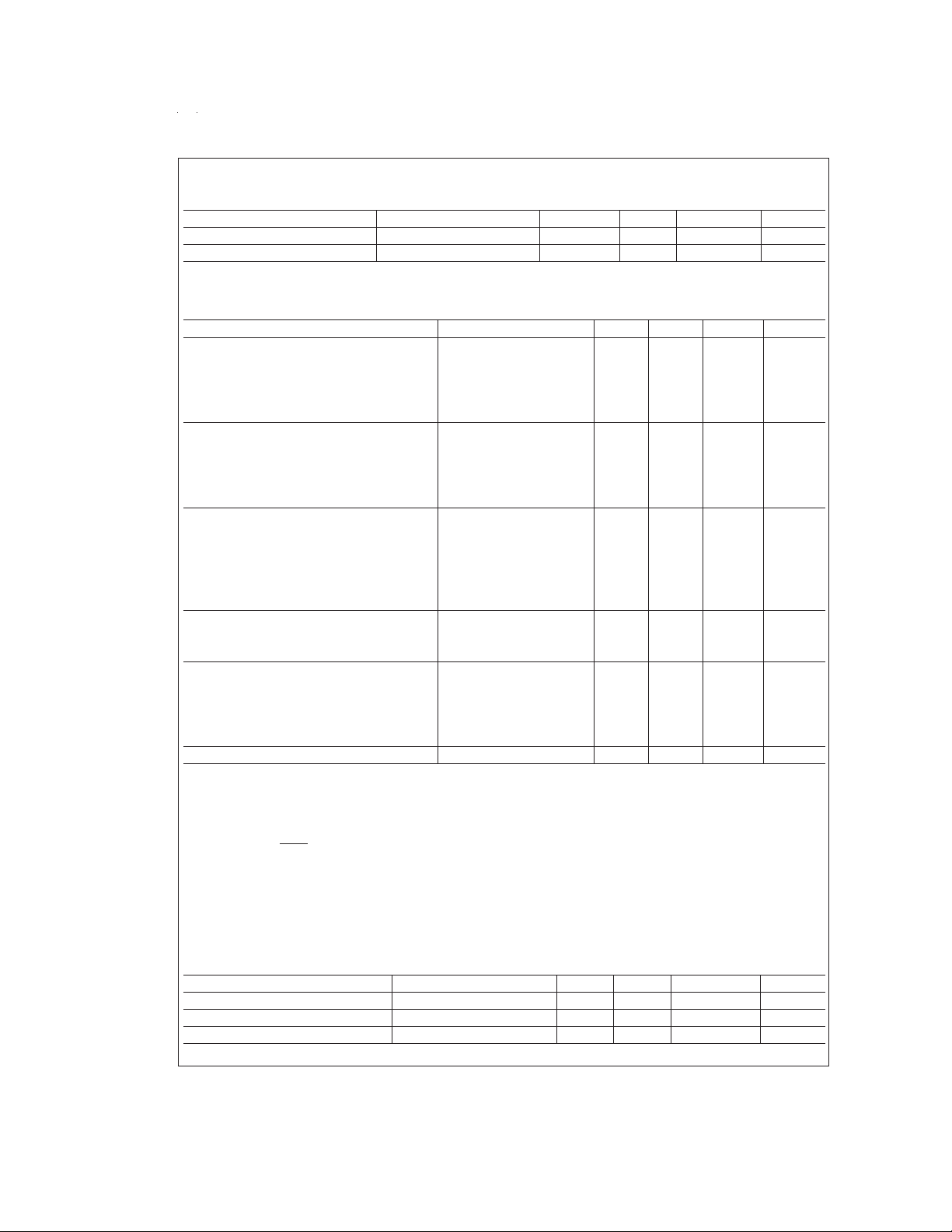
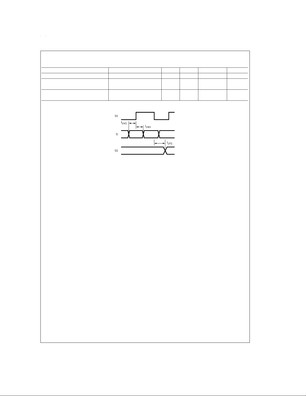
AC Electrical Characteristics
−40˚C ≤ TA≤ +85˚C unless otherwise specified
Parameter Conditions Min Typ Max Units
Instruction Cycle Time (t
Crystal Resonator or External 2.7V ≤ V
R/C Oscillator 2.7V ≤ V
Inputs
t
SETUP
t
HOLD
Output Propagation Delay R
t
PD1,tPD0
SO, SK 4.5V ≤ VCC≤ 5.5V 0.7 µs
All Others 4.5V ≤ V
MICROWIRE Setup Time (t
MICROWIRE Hold Time (t
MICROWIRE Output Propagation Delay (t
Input Pulse Width (Note 7)
Interrupt Input High Time 1 t
Interrupt Input Low Time 1 t
Timer 1, 2, 3 Input High Time 1 t
Timer 1, 2, 3 Input Low Time 1 t
Reset Pulse Width 1 µs
Note 2: Maximum rate of voltage change must be less than 0.5V/ms.
Note 3: Supply current is measured after running 2000 cycles with a square wave CKI input, CKO open, inputs at rails and outputs open.
Note 4: The HALT mode will stop CKI from oscillating in the RC and the Crystal configurations. Measurement of I
sinking current; with L, C, and G0–G5 programmed as low outputs and not driving a load; all outputs programmed low and not driving a load; all inputs tied to V
clock monitor and comparatorsdisabled. Parameter refers toHALTmodeentered via setting bit 7 of the GPort data register. Part will pull up CKI during HALTincrystal clock mode.
Note 5: Pins G6 and RESET are designed with a high voltage input network. These pins allow input voltages greater than V
to VCCwhen biased at voltages greater than VCC(the pins do not have source current when biased at a voltage below VCC). The effective resistance to VCCis 750Ω
(typical). These two pins will not latch up. The voltage at the pins must be limited to less than 14V. WARNING: Voltages in excess of 14V will cause damage to the
pins. This warning excludes ESD transients.
Note 6: Parameter characterized but not tested.
=
Note 7: t
Instruction cycle time.
c
)
c
4.5V ≤ V
4.5V ≤ V
≤ 4.5V 2.5 DC µs
CC
≤ 5.5V 1.0 DC µs
CC
<
4.0V 7.5 DC µs
CC
≤ 5.5V 3.0 DC µs
CC
4.5V ≤ VCC≤ 5.5V 200 ns
2.7V ≤ V
<
4.5V 500 ns
CC
4.5V ≤ VCC≤ 5.5V 60 ns
2.7V ≤ V
L
2.7V ≤ V
2.7V ≤ V
) (Note 6) VCC≥ 4.5V 20 ns
UWS
) (Note 6) VCC≥ 4.5V 56 ns
UWH
)VCC≥ 4.5V 220 ns
UPD
<
4.5V 150 ns
CC
=
=
2.2k, C
100 pF
L
<
4.5V 1.75 µs
CC
≤ 5.5V 1 µs
CC
<
4.5V 2.5 µs
CC
HALT is done with device neither sourcing or
DD
and the pins will have sink current
CC
c
c
c
c
;
CC
Comparators AC and DC Characteristics
=
V
5V, −40˚C ≤ T
CC
Parameter Conditions Min Typ Max Units
Input Offset Voltage 0.4V ≤ V
Input Common Mode Voltage Range 0.4 V
Low Level Output Current V
www.national.com 6
≤ +85˚C
A
≤ VCC− 1.5V
IN
=
0.4V 1.6 mA
OL
±
10
±
25 mV
− 1.5 V
CC
Comparators AC and DC Characteristics (Continued)
=
V
5V, −40˚C ≤ T
CC
Parameter Conditions Min Typ Max Units
High Level Output Current V
DC Supply Current Per Comparator 250 µA
(When Enabled)
Response Time 100 mV 1 µs
≤ +85˚C
A
=
4.6V 1.6 mA
OH
Overdrive, 100 pF Load
DS101135-18
FIGURE 3. MICROWIRE/PLUS Timing
www.national.com7
Pin Descriptions
VCCand GND are the power supply pins. All VCCand GND
pins must be connected.
CKI is the clock input. This can come from an R/C generated
oscillator, or a crystal oscillator (in conjunction with CKO).
See Oscillator Description section.
RESET is the master reset input. See Reset Description section.
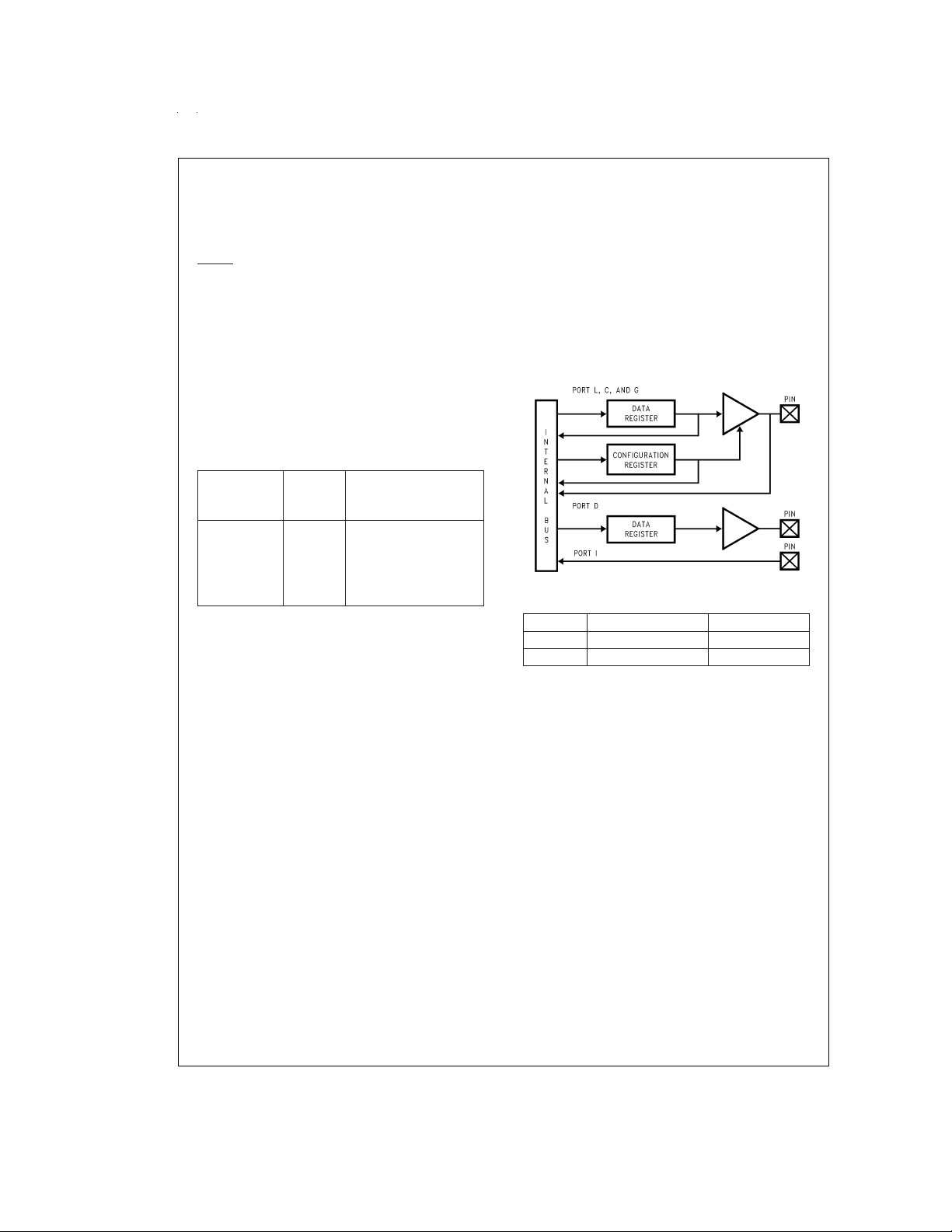
The device contains three bidirectional 8-bit I/O ports (C, G
and L), where each individual bit may be independently configured as an input (Schmitt trigger inputs on ports L and G),
output or TRI-STATE under program control. Three data
memory address locations are allocated for each of these
I/O ports. Each I/O port has two associated 8-bit memory
mapped registers, the CONFIGURATION register and the
output DATA register.A memory mapped address is also reserved for the input pins of each I/O port. (See the memory
map for the various addresses associated with the I/O ports.)
Figure 4
shows the I/O port configurations. The DATA and
CONFIGURATION registers allow for each port bit to be individually configured under software control as shown below:
CONFIGURA-
TION
Register
0 0 Hi-Z Input
0 1 Input with Weak Pull-Up
1 0 Push-Pull Zero Output
1 1 Push-Pull One Output
PORT L is an 8-bit I/O port. All L-pins have Schmitt triggers
on the inputs.
The Port L supports Multi-Input WakeUp on all eight pins. L1
is used for the USART external clock. L2 and L3 are used for
the USART transmit and receive. L4 and L5 are used for the
timer input functions T2A and T2B. L6 and L7 are used for
the timer input functions T3A and T3B.
The Port L has the following alternate features:
L7 MIWU or T3B
L6 MIWU or T3A
L5 MIWU or T2B
L4 MIWU or T2A
L3 MIWU or RDX
L2 MIWU or TDX
L1 MIWU or CKX
L0 MIWU
Port G is an 8-bit port with 5 I/O pins (G0, G2–G5), an input
pin (G6), and two dedicated output pins (G1 and G7). Pins
G0 and G2–G6 all have Schmitt Triggers on their inputs. Pin
G1 serves as the dedicated WDOUT WATCHDOG output,
while pin G7 is either input or output depending on the oscillator mask option selected. With the crystal oscillator option
selected, G7 serves as the dedicated output pin for the CKO
clock output. With the single-pin R/C oscillator mask option
selected, G7 serves as a general purpose input pin but is
also used to bring the device out of HALTmode with a low to
high transition on G7. There are two registers associated
with the G Port, a data register and a configuration register.
Therefore, each of the 5 I/O bits (G0, G2–G5) can be individually configured under software control.
DATA
Register
Port Set-Up
(TRI-STATE Output)
Since G6 is an input only pin and G7 is the dedicated CKO
clock output pin (crystal clock option) or general purpose input (R/C clock option), the associated bits in the data and
configuration registers for G6 and G7 are used for special
purpose functions as outlined below. Reading the G6 and G7
data bits will return zeros.
Note that the chip will be placed in the HALT mode by writing
a “1” to bit 7 of the Port G Data Register. Similarly the chip
will be placed in the IDLE mode by writing a “1” to bit 6 of the
Port G Data Register.
Writing a “1” to bit 6 of the Port G Configuration Register enables the MICROWIRE/PLUS to operate with the alternate
phase of the SK clock. The G7 configuration bit, if set high,
enables the clock start up delay after HALT when the R/C
clock configuration is used.
DS101135-6
FIGURE 4. I/O Port Configurations
Config Reg. Data Reg.
G7 CLKDLY HALT
G6 Alternate SK IDLE
Port G has the following alternate features:
G6 SI (MICROWIRE
™
Serial Data Input)
G5 SK (MICROWIRE Serial Clock)
G4 SO (MICROWIRE Serial Data Output)
G3 T1A (Timer T1 I/O)
G2 T1B (Timer T1 Capture Input)
G0 INTR (External Interrupt Input)
Port G has the following dedicated functions:
G7 CKO Oscillator dedicated output or general purpose
input
G1 WDOUT WATCHDOG and/or Clock Monitor dedi-
cated output
Port C is an 8-bit I/O port. The 40-pin device does not have
a full complement of Port C pins. The unavailable pins are
not terminated.A read operation for these unterminated pins
will return unpredicatable values.
PORTI isan eight-bit Hi-Z input port. The 28-pin device does
not have a full complement of Port I pins. The unavailable
pins are not terminated i.e., they are floating. A read operation for these unterminated pins will return unpredictable values. The user must ensure that the software takes this into
account by either masking or restricting the accesses to bit
operations. The unterminated Port I pins will draw power
only when addressed.
Port I1–I3 are used for Comparator 1. Port I4–I6 are used for
Comparator 2.
www.national.com 8

Pin Descriptions (Continued)
The Port I has the following alternate features.
I6 COMP2OUT (Comparator 2 Output)
I5 COMP2+IN (Comparator 2 Positive Input)
I4 COMP2−IN (Comparator 2 Negative Input)
I3 COMP1OUT (Comparator 1 Output)
I2 COMP1+IN (Comparator 1 Positive Input)
I1 COMP1−IN (Comparator 1 Negative Input)
Port D is an 8-bit output port that is preset high when RESET
goes low. The user can tie two or more D port outputs (except D2) together in order to get a higher drive.
Note: Care must be exercised with the D2 pin operation. At RESET, the ex-
ternal loads on this pin must ensure that the output voltages stay
above 0.8 V
keep the external loading on D2 to less than 1000 pF.
to prevent the chip from entering special modes. Also
CC
Functional Description
The architecture of the device is modified Harvard architecture. With the Harvard architecture, the control store program memory (ROM) is separated from the data store
memory (RAM). Both ROM and RAM have their own separate addressing space with separate address buses. The architecture, though based on Harvard architecture, permits
transfer of data from ROM to RAM.
CPU REGISTERS
The CPU can do an 8-bit addition, subtraction, logical or shift
operation in one instruction (t
There are six CPU registers:
A is the 8-bit Accumulator Register
PC is the 15-bit Program Counter Register
PU is the upper 7 bits of the program counter (PC)
PL is the lower 8 bits of the program counter (PC)
B is an 8-bit RAM address pointer, which can be optionally
post auto incremented or decremented.
X is an 8-bit alternate RAM address pointer, which can be
optionally post auto incremented or decremented.
SP is the 8-bit stack pointer, which points to the subroutine/
interrupt stack (in RAM). The SP is initialized to RAM address 06F with reset.
S is the 8-bit Data SegmentAddress Registerused to extend
the lower half of the address range (00 to 7F) into 256 data
segments of 128 bytes each.
All the CPU registers are memory mapped with the exception of the Accumulator (A) and the Program Counter (PC).
PROGRAM MEMORY
The program memory consists of 12288 bytes of ROM.
These bytes may hold program instructions or constant data
(data tables for the LAID instruction, jump vectors for the JID
instruction, and interrupt vectors for the VIS instruction). The
program memory is addressed by the 15-bit program
counter (PC). All interrupts in the devices vector to program
memory location 0FF Hex.
The device can be configured to inhibit external reads of the
program memory.This is done by programming the Security
Byte.
) cycle time.
c
SECURITY FEATURE
The program memory array has an associate Security Byte
that is located outside of the program address range. This
byte can be addressed only from programming mode by a
programmer tool.
Security is an optional feature and can only be asserted after
the memory array has been programmed and verified. A secured part will read all 00(hex) by a programmer. The part
will fail Blank Check and will fail Verify operations. A Read
operation will fill the programmer’s memory with 00(hex).
The Security Byte itself is always readable with value of
00(hex) if unsecure and FF(hex) if secure.
DATA MEMORY
The data memory address space includes the on-chip RAM
and data registers, the I/O registers (Configuration, Data and
Pin), the control registers, the MICROWIRE/PLUS SIO shift
register, and the various registers, and counters associated
with the timers (with the exception of the IDLE timer). Data
memory is addressed directly by the instruction or indirectly
by the B, X, SP pointers and S register.
The data memory consists of 512 bytes of RAM. Sixteen
bytes of RAM are mapped as “registers” at addresses 0F0 to
0FF Hex. These registers can be loaded immediately, and
also decremented and tested with the DRSZ (decrement
register and skip if zero) instruction. The memory pointer
registers X, SP,B and S are memory mapped into this space
at address locations 0FC to 0FF Hex respectively, with the
other registers being available for general usage.
The instruction set permits any bit in memory to be set, reset
or tested. All I/O and registers (except A and PC) are
memory mapped; therefore, I/O bits and register bits can be
directly and individually set, reset and tested. The accumulator (A) bits can also be directly and individually tested.
Note: RAM contents are undefined upon power-up.
Data Memory Segment RAM
Extension
Data memory address 0FF is used as a memory mapped location for the Data Segment Address Register (S).
The data store memory is either addressed directly by a
single byte address within the instruction, or indirectly relative to the reference of the B, X, or SP pointers (each contains a single-byte address). This single-byte address allows
an addressing range of 256 locations from 00 to FF hex. The
upper bit of this single-byte address divides the data store
memory into two separate sections as outlined previously.
With the exception of the RAM register memory from address locations 00F0 to 00FF, all RAM memory is memory
mapped with the upper bit of the single-byte address being
equal to zero. This allows the upper bit of the single-byte address to determine whether or not the base address range
(from 0000 to 00FF) is extended. If this upper bit equals one
(representing address range 0080 to 00FF), then address
extension does not take place. Alternatively, if this upper bit
equals zero, then the data segment extension register S is
used to extend the base address range (from 0000 to 007F)
from XX00 to XX7F, where XX represents the 8 bits from the
S register. Thus the 128-byte data segment extensions are
located from addresses 0100 to 017F for data segment 1,
0200 to 027F for data segment 2, etc., up to FF00 to FF7F
for data segment 255. The base address range from 0000 to
007F represents data segment 0.
www.national.com9
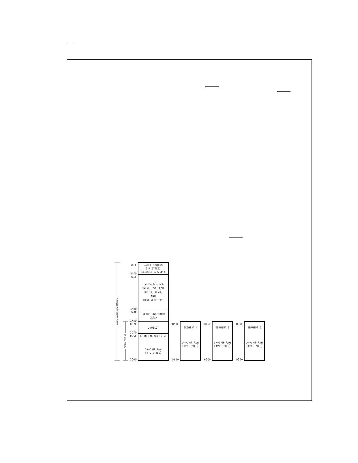
Data Memory Segment RAM
Extension
Figure 5
sion is used in extending the lower half of the base address
range (00 to 7F hex) into 256 data segments of 128 bytes
each, with a total addressing range of 32 kbytes from XX00
to XX7F. This organization allows a total of 256 data segments of 128 bytes each with an additional upper base segment of 128 bytes. Furthermore, all addressing modes are
available for all data segments. The S register must be
changed under program control to move from one data segment (128 bytes) to another. However, the upper base segment (containing the 16 memory registers, I/O registers,
control registers, etc.) is always available regardless of the
contents of the S register, since the upper base segment
(address range 0080 to 00FF) is independent of data segment extension.
The instructions that utilize the stack pointer (SP) always reference the stack as part of the base segment (Segment 0),
regardless of the contents of the S register. The S register is
not changed by these instructions. Consequently, the stack
(used with subroutine linkage and interrupts) is always located in the base segment. The stack pointer will be intitialized to point at data memory location 006F as a result of reset.
The 128 bytes of RAM contained in the base segment are
split between the lower and upper base segments. The first
112bytes of RAM are resident from address 0000 to 006F in
the lower base segment, while the remaining 16 bytes of
RAM represent the 16 data memory registers located at addresses 00F0 to 00FF of the upper base segment. No RAM
is located at the upper sixteen addresses (0070 to 007F) of
the lower base segment.
Additional RAM beyond these initial 128 bytes, however, will
always be memory mapped in groups of 128 bytes (or less)
at the data segment address extensions (XX00 to XX7F) of
(Continued)
illustrates how the S register data memory exten-
the lower base segment. The additional 128 bytes of RAM
are memory mapped at address locations 0100 to 017F hex.
Reset
The RESET input when pulled low initializes the microcontroller. Initialization will occur whenever the RESET input is
pulled low. Upon initialization, the data and configuration
registers for ports L, G and C are cleared, resulting in these
Ports being initialized to the TRI-STATE mode. Pin G1 of the
G Port is an exception (as noted below) since pin G1 is dedicated as the WATCHDOG and/or Clock Monitor error output
pin. Port D is set high. The PC, PSW, ICNTRL, CNTRL,
T2CNTRL and T3CNTRL control registers are cleared. The
USART registers PSR, ENU (except that TBMT bit is set),
ENUR and ENUI are cleared. The Comparator Select Register is cleared. The S register is initialized to zero. The
Multi-Input Wakeup registers WKEN, WKEDG and WKPND
are cleared. (Wakeup register WKPND is unknown.) The
stack pointer, SP, is initialized to 6F Hex.
The device comes out of reset with both the WATCHDOG
logic and the Clock Monitor detector armed, with the
WATCHDOG service window bits set and the Clock Monitor
bit set. The WATCHDOG and Clock Monitor circuits are inhibited during reset. The WATCHDOG service window bits
being initialized high default to the maximum WATCHDOG
service window of 64k t
being initialized high will cause a Clock Monitor error following reset if the clock has not reached the minimum specified
frequency at the termination of reset. A Clock Monitor error
will cause an active low error output on pin G1. This error
output will continue until 16 t
the clock frequency reaching the minimum specified value,
at which time the G1 output will enter the TRI-STATE mode.
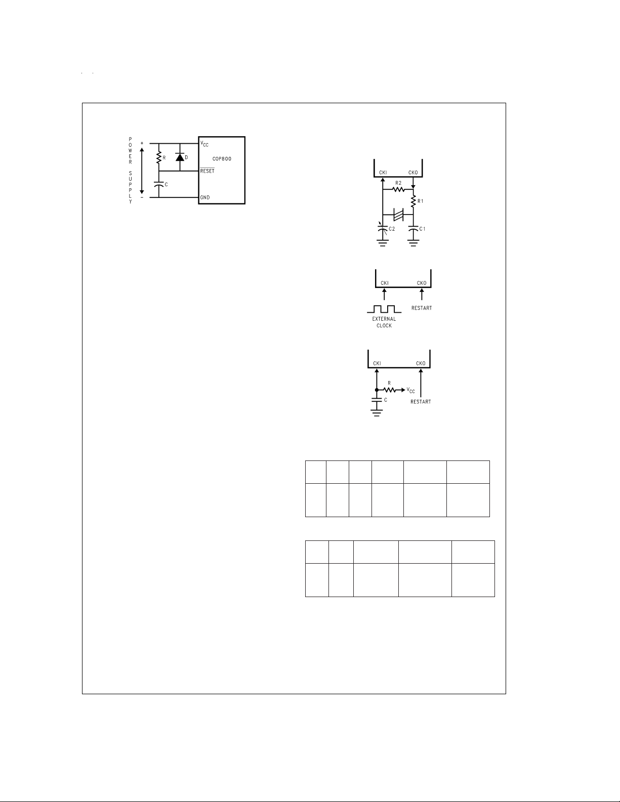
The external RC network shown in
to ensure that the RESET pin is held low until the power supply to the chip stabilizes.
clock cycles. The Clock Monitor bit
C
–32 tCclock cycles following
C
Figure 6
should be used
*Reads as all ones.
FIGURE 5. RAM Organization
www.national.com 10
DS101135-7
Reset (Continued)
EXTERNAL OSCILLATOR
CKI can be driven by an external clock signal. CKO is available as a general purpose input and/or HALT restart control.
Crystal Oscillator
RC>5 x Power Supply Rise Time
DS101135-8
FIGURE 6. Recommended Reset Circuit
Oscillator Circuits
The chip can be driven by a clock input on the CKI input pin
which can be between DC and 10 MHz. The CKO output
clock is on pin G7 (crystal configuration). The CKI input frequency is divided down by 10 to produce the instruction
cycle clock (t
Figure 7
CRYSTAL OSCILLATOR
CKI and CKO can be connected to make a closed loop crystal (or resonator) controlled oscillator.
Table 1
standard crystal values.
R/C OSCILLATOR
By selecting CKI as a single pin oscillator input, a single pin
R/C oscillator circuit can be connected to it. CKO is available
as a general purpose input, and/or HALT restart input.
Table 2
functions of the component (R and C) values.
).
c
shows the Crystal and R/C oscillator diagrams.
shows the component values required for various
shows the variation in the oscillator frequencies as
DS101135-9
External Oscillator
DS101135-10
R/C Oscillator
DS101135-11
FIGURE 7. Crystal R/C, and
External Oscillator Diagrams
TABLE 1. Crystal Oscillator Configuration, T
R1 R2 C1 C2 CKI Freq
(kΩ)(MΩ) (pF) (pF) (MHz)
0 1 30 30–36 10 V
0 1 30 30–36 4 V
0 1 200 100–150 0.455 V
=
25˚C
A
Conditions
=
5V
CC
=
5V
CC
=
5V
CC
TABLE 2. RC Oscillator Configuration, T
R C CKI Freq Instr. Cycle
(kΩ) (pF) (MHz) (µs)
3.3 82 2.2 to 2.7 3.7 to 4.6 V
5.6 100 1.1 to 1.3 7.4 to 9.0 V
6.8 100 0.9 to 1.1 8.8 to 10.8 V
Note: 3k ≤ R ≤ 200k
50 pF ≤ C ≤ 200 pF
=
25˚C
A
Conditions
=
CC
=
CC
=
CC
www.national.com11
5V
5V
5V
Control Registers
CNTRL Register (Address X'00EE)
T1C3 T1C2 T1C1 T1C0 MSEL IEDG SL1 SL0
Bit 7 Bit 0
The Timer1 (T1) and MICROWIRE/PLUS control register
contains the following bits:
T1C3 Timer T1 mode control bit
T1C2 Timer T1 mode control bit
T1C1 Timer T1 mode control bit
T1C0 Timer T1 Start/Stop control in timer
modes 1 and 2, T1 Underflow Interrupt
Pending Flag in timer mode 3
MSEL Selects G5 and G4 as MICROWIRE/PLUS
signals SK and SO respectively
IEDG External interrupt edge polarity select
(0 = Rising edge, 1 = Falling edge)
SL1 & SL0 Select the MICROWIRE/PLUS clock divide
by (00 = 2, 01 = 4, 1x = 8)
PSW Register (Address X'00EF)
HC C T1PNDA T1ENA EXPND BUSY EXEN GIE
Bit 7 Bit 0
The PSW register contains the following select bits:
HC Half Carry Flag
C Carry Flag
T1PNDA Timer T1 Interrupt Pending Flag (Autoreload
RA in mode 1, T1 Underflow in Mode 2, T1A
capture edge in mode 3)
T1ENA Timer T1 Interrupt Enable for Timer Underflow
or T1A Input capture edge
EXPND External interrupt pending
BUSY MICROWIRE/PLUS busy shifting flag
EXEN Enable external interrupt
GIE Global interrupt enable (enables interrupts)
The Half-Carry flag is also affected by all the instructions that
affect the Carry flag. The SC (Set Carry) and R/C (Reset
Carry) instructions will respectively set or clear both the carry
flags. In addition to the SC and R/C instructions, ADC,
SUBC, RRC and RLC instructions affect the Carry and Half
Carry flags.
ICNTRL Register (Address X'00E8)
Reserved LPEN T0PND T0EN µWPND µWEN T1PNDB T1ENB
Bit 7 Bit 0
The ICNTRL register contains the following bits:
Reserved This bit is reserved and must be zero.
LPEN L Port Interrupt Enable (Multi-Input Wakeup/
Interrupt)
T0PND Timer T0 Interrupt pending
T0EN Timer T0 Interrupt Enable (Bit 12 toggle)
µWPND MICROWIRE/PLUS interrupt pending
µWEN Enable MICROWIRE/PLUS interrupt
T1PNDB Timer T1 Interrupt Pending Flag for T1B cap-
ture edge
T1ENB Timer T1 Interrupt Enable for T1B Input cap-
ture edge
T2CNTRL Register (Address X'00C6)
T2C3 T2C2 T2C1 T2C0 T2PNDA T2ENA T2PNDB T2ENB
Bit 7 Bit 0
The T2CNTRL control register contains the following bits:
T2C3 Timer T2 mode control bit
T2C2 Timer T2 mode control bit
T2C1 Timer T2 mode control bit
T2C0 Timer T2 Start/Stop control in timer
modes 1 and 2, T2 Underflow Interrupt Pend-
ing Flag in timer mode 3
T2PNDA Timer T2 Interrupt Pending Flag (Autoreload
RA in mode 1, T2 Underflow in mode 2, T2A
capture edge in mode 3)
T2ENA Timer T2 Interrupt Enable for Timer Underflow
or T2A Input capture edge
T2PNDB Timer T2 Interrupt Pending Flag for T2B cap-
ture edge
T2ENB Timer T2 Interrupt Enable for Timer Underflow
or T2B Input capture edge
T3CNTRL Register (Address X'00B6)
T3C3 T3C2 T3C1 T3C0 T3PNDA T3ENA T3PNDB T3ENB
Bit 7 Bit 0
The T3CNTRL control register contains the following bits:
T3C3 Timer T3 mode control bit
T3C2 Timer T3 mode control bit
T3C1 Timer T3 mode control bit
T3C0 Timer T3 Start/Stop control in timer
modes 1 and 2, T3 Underflow Interrupt Pend-
ing Flag in timer mode 3
T3PNDA Timer T3 Interrupt Pending Flag (Autoreload
RA in mode 1, T3 Underflow in mode 2, T3A
capture edge in mode 3)
T3ENA Timer T3 Interrupt Enable for Timer Underflow
or T3A Input capture edge
T3PNDB Timer T3 Interrupt Pending Flag for T3B cap-
ture edge
T3ENB Timer T3 Interrupt Enable for Timer Underflow
or T3B Input capture edge
www.national.com 12
Timers
The device contains a very versatile set of timers (T0, T1,
T2, T3). All timers and associated autoreload/capture registers power up containing random data.
TIMER T0 (IDLE TIMER)
The device supports applications that require maintaining
real time and low power with the IDLE mode. This IDLE
mode support is furnished by the IDLE timer T0, which is a
16-bit timer.The TimerT0 runs continuously at the fixed rate
of the instruction cycle clock, t
write to the IDLE Timer T0, which is a count down timer.
The Timer T0 supports the following functions:
Exit out of the Idle Mode (See Idle Mode description)
•
WATCHDOG logic (See WATCHDOG description)
•
Start up delay out of the HALT mode
•
The IDLE Timer T0 can generate an interrupt when the thirteenth bit toggles. This toggle is latched into the T0PND
pending flag, and will occur every 4 ms at the maximum
clock frequency (t
terrupt from the thirteenth bit of Timer T0 to be enabled or
=
1 µs). Acontrol flag T0EN allows the in-
c
disabled. Setting T0EN will enable the interrupt, while resetting it will disable the interrupt.
TIMER T1, TIMER T2 AND TIMER T3
The device has a set of three powerful timer/counter blocks,
T1, T2 and T3. The associated features and functioning of a
timer block are described by referring to the timer block Tx.
Since the three timer blocks, T1, T2 and T3 are identical, all
comments are equally applicable to any of the three timer
blocks.
Each timer block consists of a 16-bit timer, Tx, and two supporting 16-bit autoreload/capture registers, RxA and RxB.
Each timer block has two pins associated with it, TxA and
TxB. The pin TxA supports I/O required by the timer block,
while the pin TxB is an input to the timer block. The powerful
and flexible timer block allows the device to easily perform all
timer functions with minimal software overhead. The timer
block has three operating modes: Processor Independent
PWM mode, External Event Counter mode, and Input Capture mode.
The control bits TxC3, TxC2, and TxC1 allow selection of the
different modes of operation.
Mode 1. Processor Independent PWM Mode
As the name suggests, this mode allows the device to generate a PWM signal with very minimal user intervention. The
user only has to define the parameters of the PWM signal
(ON time and OFF time). Once begun, the timer block will
continuously generate the PWM signal completely independent of the microcontroller. The user software services the
timer block only when the PWM parameters require updating.
In this mode the timer Tx counts down at a fixed rate of t
Upon every underflow the timer is alternately reloaded with
the contents of supporting registers, RxA and RxB. The very
first underflow of the timer causes the timer to reload from
the register RxA. Subsequent underflows cause the timer to
be reloaded from the registers alternately beginning with the
register RxB.
The Tx Timer control bits, TxC3, TxC2 and TxC1 set up the
timer for PWM mode operation.
Figure 8
shows a block diagram of the timer in PWM mode.
. The user cannot read or
c
The underflows can be programmed to toggle the TxAoutput
pin. The underflows can also be programmed to generate interrupts.
Underflows from the timer are alternately latched into two
pending flags, TxPNDA and TxPNDB. The user must reset
these pending flags under software control. Two control enable flags, TxENA and TxENB, allow the interrupts from the
timer underflow to be enabled or disabled. Setting the timerenable flag TxENA will cause an interrupt when a timer underflow causes the RxA registerto be reloaded into the timer.
Setting the timer enable flag TxENB will cause an interrupt
when a timer underflow causes the RxB register to be reloaded into the timer. Resetting the timer enable flags will
disable the associated interrupts.
Either or both of the timer underflow interrupts may be enabled. This gives the user the flexibility of interrupting once
per PWM period on either the rising or falling edge of the
PWM output. Alternatively, the user may choose to interrupt
on both edges of the PWM output.
FIGURE 8. Timer in PWM Mode
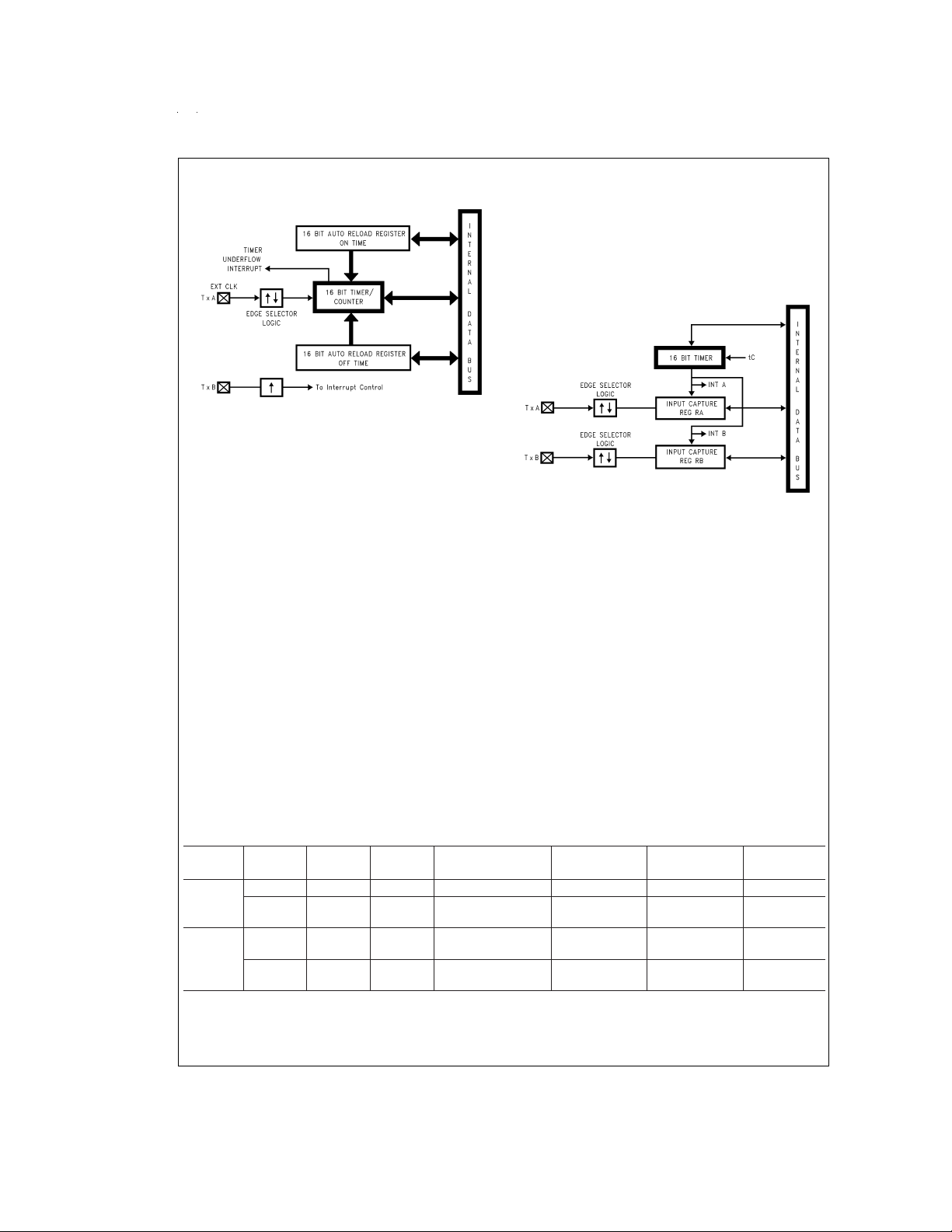
Mode 2. External Event Counter Mode
This mode is quite similar to the processor independent
PWM mode described above. The main difference is that the
timer,Tx, is clocked by the input signal from the TxA pin. The
Tx timer control bits,TxC3, TxC2 and TxC1 allow the timer to
be clocked either on a positive or negative edge from the
TxA pin. Underflows from the timer are latched into the TxPNDA pending flag. Setting the TxENA control flag will cause
an interrupt when the timer underflows.
In this mode the input pin TxB can be used as an independent positive edge sensitive interrupt input if the TxENB control flag is set. The occurrence of a positive edge on the TxB
input pin is latched into the TxPNDB flag.
Figure 9
shows a block diagram of the timer in External
Event Counter mode.
Note: The PWM output is notavailable in this mode since the TxApinisbeing
used as the counter input clock.
.
c
DS101135-12
www.national.com13
Timers (Continued)
sequently, the TxC0 control bit should be reset when entering the Input Capture mode. The timer underflow interrupt is
enabled with the TxENA control flag. When a TxA interrupt
occurs in the Input Capture mode, the user must check both
the TxPNDA and TxC0 pending flags in order to determine
whether a TxA input capture or a timer underflow (or both)
caused the interrupt.
Figure 10
ture mode.
DS101135-13
FIGURE 9. Timer in External Event Counter Mode
Mode 3. Input Capture Mode
The device can precisely measure external frequencies or
time external events by placing the timer block, Tx, in the input capture mode.
In this mode, the timer Tx is constantly running at the fixed t
rate. The two registers, RxA and RxB, act as capture registers. Each register acts in conjunction with a pin. The register
RxAacts in conjunction withthe TxApin and the register RxB
acts in conjunction with the TxB pin.
The timer value gets copied over into the register when a
trigger event occurs on its corresponding pin. Control bits,
TxC3, TxC2 and TxC1, allow the trigger events to be specified either as a positive or a negative edge. The trigger condition for each input pin can be specified independently.
c
TIMER CONTROL FLAGS
The control bits and their functions are summarized below.
TxC3 Timer mode control
TxC2 Timer mode control
TxC1 Timer mode control
TxC0 Timer Start/Stop control in Modes 1 and 2 (Pro-
The trigger conditions can also be programmed to generate
interrupts. The occurrence of the specified trigger condition
on the TxA and TxB pins will be respectively latched into the
pending flags, TxPNDA and TxPNDB. The control flag TxENA allows the interrupt on TxA to be either enabled or disabled. Setting the TxENA flagenables interrupts to be generated when the selected trigger condition occurs on the TxA
TxPNDA Timer Interrupt Pending Flag
TxENA Timer Interrupt Enable Flag
pin. Similarly, the flag TxENB controls the interrupts from the
TxB pin.
Underflows from the timer can also be programmed to generate interrupts. Underflows are latched into the timer TxC0
TxPNDB Timer Interrupt Pending Flag
TxENB Timer Interrupt Enable Flag
pending flag (the TxC0 control bit serves as the timer underflow interrupt pending flag in the Input Capture mode). Con-
The timer mode control bits (TxC3, TxC2 and TxC1) are detailed below:
shows a block diagram of the timer in Input Cap-
DS101135-14
FIGURE 10. Timer in Input Capture Mode
cessor Independent PWM and External Event
Counter), where 1 = Start, 0 = Stop
Timer Underflow Interrupt Pending Flag in
Mode 3 (Input Capture)
1 = Timer Interrupt Enabled
0 = Timer Interrupt Disabled
1 = Timer Interrupt Enabled
0 = Timer Interrupt Disabled
Mode TxC3 TxC2 TxC1 Description
1 0 1 PWM: TxA Toggle Autoreload RA Autoreload RB t
1
1 0 0 PWM: No TxA
Toggle
0 0 0 External Event
2
0 0 1 External Event
Counter
Counter
www.national.com 14
Interrupt A
Source
Interrupt B
Source
Autoreload RA Autoreload RB
Timer
Pos. TxB Edge Pos. TxA
Underflow
Timer
Pos. TxB Edge Pos. TxA
Underflow
Timer
Counts On
C
t
C
Edge
Edge
 Loading...