

查询COP87L20CJM-1N供应商
COP820CJ/COP822CJ/COP823CJ 8-Bit Microcontroller
with Multi-Input Wake Up and Brown Out Detector
General Description
The COP820CJ is a member of the COP8TM8-bit Microcontroller family. It is a fully static Microcontroller, fabricated
using double-metal silicon gate microCMOS technology.
This low cost Microcontroller is a complete microcomputer
containing all system timing, interrupt logic, ROM, RAM, and
I/O necessary to implement dedicated control functions in a
variety of applications. Features include an 8-bit memory
mapped architecture, MICROWIRE
timer/counter with capture register, a multi-sourced interrupt, Comparator, WATCHDOG
Brown out protection and Multi-Input Wakeup. Each I/O pin
has software selectable options to adapt the device to the
specific application. The device operates over a voltage
range of 2.5V to 6.0V. High throughput is achieved with an
efficient, regular instruction set operating at a 1 ms per instruction rate.
Key Features
Y
Multi-Input Wake Up (on the 8-bit Port L)
Y
Brown out detector
Y
Analog comparator
Y
Modulator/timer (High speed PWM for IR transmission)
Y
16-bit multi-function timer supporting
Ð PWM mode
Ð External event counter mode
Ð Input capture mode
Y
1024 bytes of ROM
Y
64 bytes of RAM
I/O Features
Y
Memory mapped I/O
TM
TM
serial I/O, a 16-bit
Timer, Modulator/Timer,
September 1996
Y
Software selectable I/O options (TRI-STATEÉoutput,
push-pull output, weak pull-up input, high impedance
input)
Y
High current outputs (8 pins)
Y
Schmitt trigger inputs on Port G
Y
MICROWIRE/PLUSTMserial I/O
Y
Packages
Ð 16 SO with 12 I/O pins
Ð 20 DIP/SO with 16 I/O pins
Ð 28 DIP/SO with 24 I/O pins
CPU/Instruction Set Feature
Y
1 ms instruction cycle time
Y
Three multi-source vectored interrupts servicing
Ð External interrupt with selectable edge
Ð Timer interrupt
Ð Software interrupt
Y
Versatile and easy to use instruction set
Y
8-bit Stack Pointer (SP)Ðstack in RAM
Y
Two 8-bit register indirect data memory pointers (B, X)
Fully Static CMOS
Y
Low current drain (typicallyk1 mA)
Y
Single supply operation: 2.5V to 6.0V
Y
Temperature range:b40§Ctoa85§C
Development Support
Y
Emulation and OTP devices
Y
Real time emulation and full program debug offered by
MetaLink Development System
COP820CJ/COP822CJ/COP823CJ 8-Bit Microcontroller
with Multi-Input Wake Up and Brown Out Detector
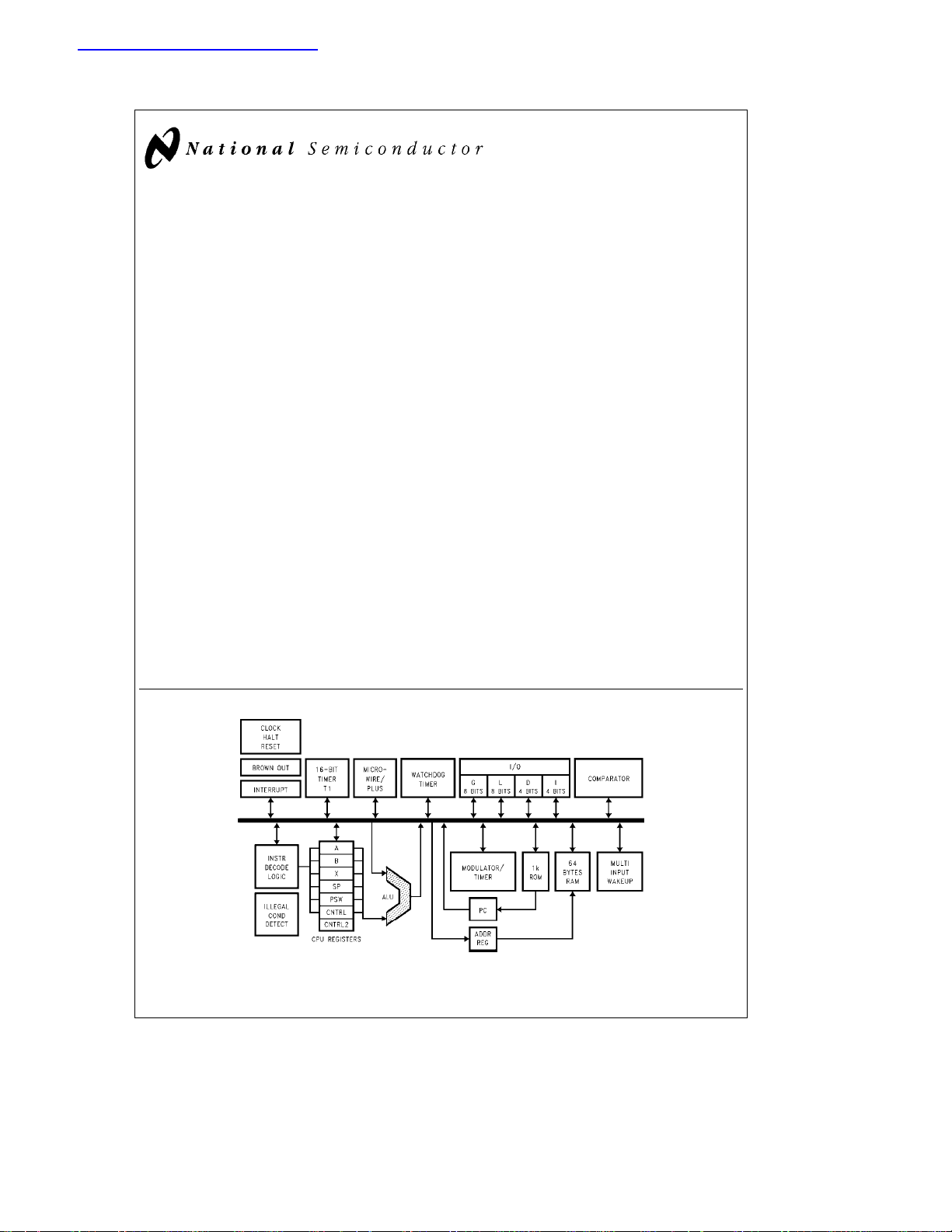
Block Diagram
FIGURE 1. Block Diagram
TRI-STATEÉis a registered trademark of National Semiconductor Corporation.
TM
COP8
Microcontrollers, MICROWIRETM, MICROWIRE/PLUSTMand WATCHDOGTMare trademarks of National Semiconductor Corporation.
TM
iceMASTER
C
1996 National Semiconductor Corporation RRD-B30M106/Printed in U. S. A.
is a trademark of MetaLink Corporation.
TL/DD11208
TL/DD/11208– 1
http://www.national.com
COP820CJ/COP822CJ/COP823CJ
Absolute Maximum Ratings
If Military/Aerospace specified devices are required,
please contact the National Semiconductor Sales
Office/Distributors for availability and specifications.
Supply Voltage (V
Voltage at any Pin
) 7.0V
CC
b
0.3V to V
CC
a
0.3V
Total Current into VCCpin (Source) 80 mA
DC Electrical Characteristics
b
40§CsT
Parameter Conditions Min Typ Max Units
Operating Voltage Brown Out Disabled 2.5 6.0 V
Power Supply Ripple 1 (Note 1) Peak to Peak 0.1 V
Supply Current (Note 2)
e
10 MHz V
CKI
e
4 MHz V
CKI
e
4 MHz V
CKI
CKIe1 MHz V
HALT Current with Brown Out
Disbled (Note 3)
HALT Current with Brown Out V
Enabled
e
6V, tce1 ms 6.0 mA
CC
e
6V, tce2.5 ms 3.5 mA
CC
e
4.0V, tce2.5 ms 2.0 mA
CC
e
4.0V, tce10 ms 1.5 mA
CC
e
6V, CKIe0 MHz
V
CC
e
6V, CKIe0 MHz
CC
Brown Out Trip Level
(Brown Out Enabled)
INPUT LEVELS (VIH,VIL)
Reset, CKI:
Logic High 0.8 V
Logic Low 0.2 V
All Other Inputs
Logic High 0.7 V
Logic Low 0.2 V
Hi-Z Input Leakage V
Input Pullup Current V
CC
CC
e
e
6.0V
6.0V, V
IN
L- and G-Port Hysteresis (Note 5) 0.35 V
Output Current Levels
D Outputs:
e
Source V
Sink V
L4–L7 Output Sink V
All Others
Source (Weak Pull-up Mode) V
Source (Push-pull Mode) V
Sink (Push-pull Mode) V
TRI-STATE Leakage
4.5V, V
CC
e
V
CC
e
CC
e
V
CC
e
CC
e
CC
e
V
CC
e
CC
e
V
CC
e
CC
e
V
CC
2.5V, V
4.5V, V
2.5V, V
4.5V, V
4.5V, V
2.5V, V
4.5V, V
2.5V, V
4.5V, V
2.5V, V
OH
OH
OL
OH
OL
OH
OH
OH
OH
OL
OL
Allowable Sink/Source
Current Per Pin
D Outputs 15 mA
L4–L7 (Sink) 20 mA
All Others 3mA
Total Current out of GND pin (sink) 80 mA
Storage Temperature Range
Absolute maximum ratings indicate limits beyond
Note:
b
65§Ctoa150§C
which damage to the device may occur.
DC and AC electrical specifications are not ensured when
operating the device at absolute maximum ratings.
s
a
85§C unless otherwise specified
A
CC
k
110 mA
k
50 110 mA
1.8 3.1 4.2 V
CC
CC
b
2
e
0V
e
3.8V
e
1.8V
e
1.0V 10 mA
e
0.4V 2 mA
e
2.5V 15 mA
e
3.2V
e
1.8V
e
3.8V
e
1.8V
e
0.4V 1.6 mA
e
0.4V 0.7 mA
b
40
b
0.4 mA
b
0.2 mA
b
10
b
2.5
b
0.4 mA
b
0.2 mA
b
2.0
CC
CC
a
2 mA
b
250 mA
CC
b
110 mA
b
33 mA
a
2.0 mA
V
V
V
V
V
V
http://www.national.com 2
DC Electrical Characteristics
b
40§CsT
s
a
85§C unless otherwise specified (Continued)
A
Parameter Conditions Min Typ Max Units
Maximum Input Current Room Temperature
without Latchup (Note 4)
RAM Retention Voltage, V
r
500 ns Rise and
Fall Time (Min)
2.0 V
g
100 mA
Input Capacitance 7pF
Load Capacitance on D2 1000 pF
Note 1: Rate of voltage change must be less than 10 V/mS.
Note 2: Supply current is measured after running 2000 cycles with a square wave CKI input, CKO open, inputs at rails and outputs open.
Note 3: The HALT mode will stop CKI from oscillating in the RC and crystal configurations. HALT test conditions: L, and G0..G5 ports configured as outputs and set
high. The D port set to zero. All inputs tied to V
Note 4: Pins G6 and RESET
when biased at voltages greater than VCC(the pins do not have source current when biased at a voltage below VCC). The effective resistance to VCCis 750X
V
CC
(typical). These two pins will not latch up. The voltage at the pins must be limited to less than 14V.
are designed with a high voltage input network. These pins allow input voltages greater than VCCand the pins will have sink current to
. The comparator and the Brown Out circuits are disabled.
CC
AC Electrical Characteristics
b
40§CsT
s
a
85§C unless otherwise specified
A
Parameter Conditions Min Typ Max Units
Instruction Cycle Time (tc)
s
Crystal/Resonator 4.5V
R/C Oscillator 4.5V
VCCRise Time when Using Brown Out V
Frequency at Brown Out Reset 4 MHz
s
V
6.0V 1 DC ms
CC
s
s
2.5V
V
4.5V 2.5 DC ms
CC
s
s
V
6.0V 3 DC ms
CC
s
s
2.5V
V
4.5V 7.5 DC ms
CC
e
0V to 6V 50 ms
CC
CKI Frequency For Modular Output 4 MHz
CKI Clock Duty Cycle (Note 5) freMax 40 60 %
Rise Time (Note 5) fr
Fall Time (Note 5) fr
e
10 MHz ext. Clock 12 ns
e
10 MHz ext. Clock 8 ns
Inputs
t
Setup
t
Hold
Output Propagation Delay R
t
PD1,tPD0
SO, SK 4.5VsV
4.5VsV
2.5V
4.5VsV
2.5V
L
2.5VsV
All Others 4.5V
2.5V
s
6.0V 200 ns
CC
s
s
V
4.5V 500 ns
CC
s
6.0V 60 ns
CC
s
s
V
4.5V 150 ns
CC
e
2.2k, CLe100 pF
s
6.0V 0.7 ms
CC
s
4.5V 1.75 ms
CC
s
s
V
6.0V 1 ms
CC
s
s
V
4.5V 5 ms
CC
Input Pulse Width
Interrupt Input High Time 1 tc
Interrupt Input Low Time 1 tc
Timer Input High Time 1 tc
Timer Input Low Time 1 tc
MICROWIRE Setup Time (t
MICROWIRE Hold Time (t
MICROWIRE Output
Propagation Delay (t
mPD
)20ns
mWS
)56ns
mWH
)
220 ns
Reset Pulse Width 1.0 ms
Note 5: Parameter characterized but not production tested.
http://www.national.com3
AC Electrical Characteristics (Continued)
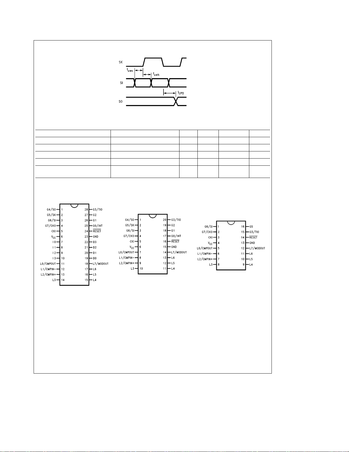
FIGURE 2. MICROWIRE/PLUS Timing
TL/DD/11208– 2
Comparator DC and AC Characteristics 4V
s
s
V
6V,b40§CsT
CC
s
A
a
85§C (Note 1)
Parameters Conditions Min Type Max Units
k
Input Offset Voltage 0.4VkV
IN
b
V
1.5V
CC
Input Common Mode Voltage Range 0.4 V
g
10
g
25 mV
b
1.5 V
CC
Voltage Gain 300k V/V
DC Supply Current (when enabled) V
Response Time TBD mV Step,
Note 1: For comparator output current characteristics see L-Port specs.
e
6.0V 250 mA
CC
TBD mV Overdrive, 100 pF Load
1 ms
Connection Diagrams
Top View
Top View
TL/DD/11208– 3
Order Number COPCJ822-XXX/N or
COPCJ822-XXX/WM
Order Number COPCJ820-XXX/N or
COPCJ820-XXX/WM
FIGURE 3. Connection Diagrams
http://www.national.com 4
TL/DD/11208– 4
Top View
TL/DD/11208– 5
Order Number COPCJ823-XXX/WM
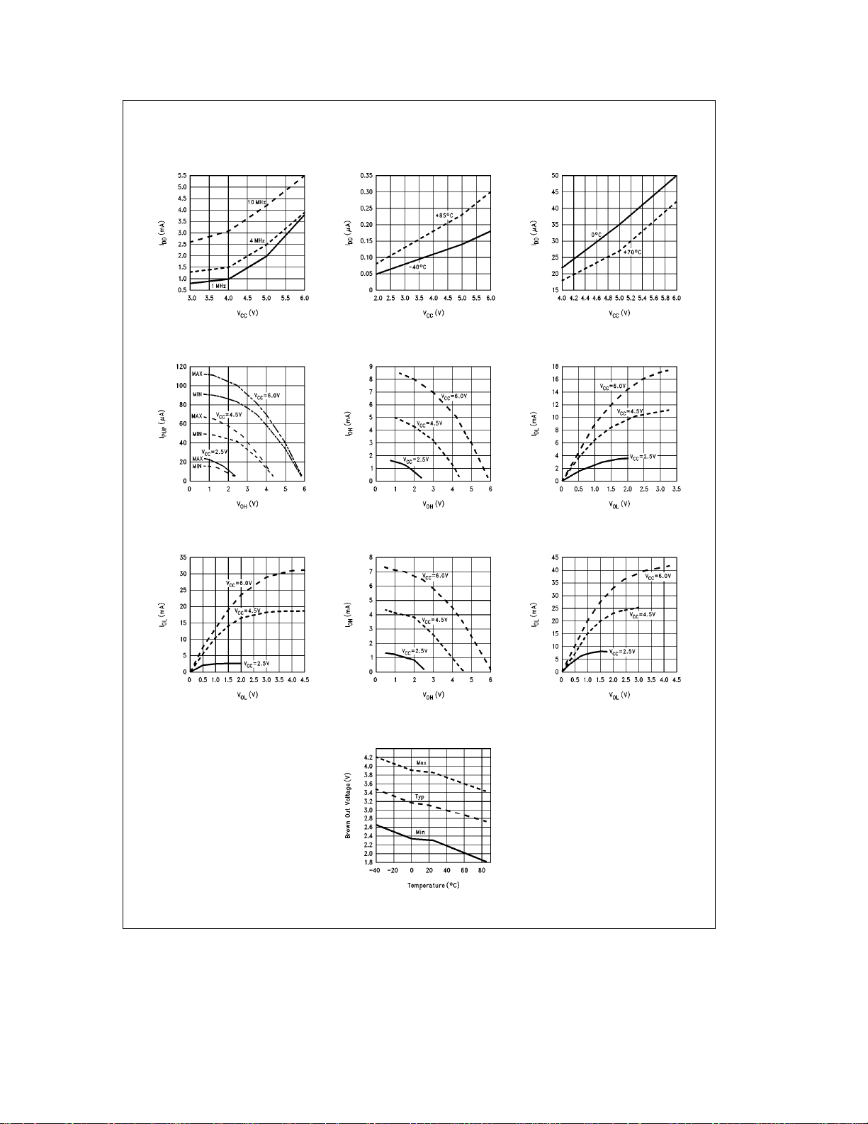
Typical Performance Characteristics
DynamicÐI
(Crystal Clock Option)
DD
vs V
CC
Ports L/G Weak
Pull-Up Source Current
Ports L4–L7
Sink Current
DD
vs V
CC
HaltÐI
(Brown Out Disabled)
Ports L/G Push-Pull
Source Current
HaltÐI
(Brown Out Enabled)
Ports L/G Push-Pull
Sink Current
DD
vs V
CC
Port D Source Current Port D Sink Current
Brown Out Voltage
vs Temperature
TL/DD/11208– 28
http://www.national.com5
COP820CJ Pin Assignment
Port
Typ
Pin Funct. Pin Pin Pin
L0 I/O MIWU/CMPOUT 5 7 11
L1 I/O MIWU/CMPIN
L2 I/O MIWU/CMPIN
L3 I/O MIWU 8 10 14
L4 I/O MIWU 9 11 15
L5 I/O MIWU 10 12 16
L6 I/O MIWU 11 13 17
L7 I/O MIWU/MODOUT 12 14 18
G0 I/O INTR 17 25
G1 I/O 18 26
G2 I/O 19 27
G3 I/O TIO 15 20 28
G4 I/O SO 1 1
G5 I/O SK 16 2 2
G6 ISI 133
G7 I CKO 2 4 4
I0 I 7
I1 I 8
I2 I 9
I3 I 10
D0 O 19
D1 O 20
D2 O 21
D3 O 22
V
CC
GND 13 15 23
CKI 3 5 5
RESET 14 16 24
ALT 16 20 28
b
6812
a
7913
466
Pin Description
VCCand GND are the power supply pins.
CKI is the clock input. This can come from an external
source, a R/C generated oscillator or a crystal (in conjunction with CKO). See Oscillator description.
RESET
is the master reset input. See Reset description.
PORT I is a 4-bit Hi-Z input port.
PORT L is an 8-bit I/O port.
There are two registers associated with the L port: a data
register and a configuration register. Therefore, each L
I/O bit can be individually configured under software control
as shown below:
Port L Port L Port L
Config. Data Setup
0 0 Hi-Z Input (TRI-STATE)
0 1 Input with Weak Pull-up
1 0 Push-pull Zero Output
1 1 Push-pull One Output
Three data memory address locations are allocated for this
port, one each for data register[00D0], configuration register[00D1]and the input pins[00D2].
Port L has the following alternate features:
L0 MIWU or CMPOUT
L1 MIWU or CMPIN
L2 MIWU or CMPIN
L3 MIWU
L4 MIWU (high sink current capability)
L5 MIWU (high sink current capability)
L6 MIWU (high sink current capability)
L7 MIWU or MODOUT (high sink current capability)
The selection of alternate Port L functions is done through
registers WKEN[00C9]to enable MIWU and CNTRL2
[
00CC]to enable comparator and modulator.
All eight L-pins have Schmitt Triggers on their inputs.
PORT G is an 8-bit port with 6 I/O pins (G0–G5) and 2 input
pins (G6, G7).
All eight G-pins have Schmitt Triggers on the inputs.
There are two registers associated with the G port: a data
register and a configuration register. Therefore each G port
bit can be individually configured under software control as
shown below:
Port G Port G Port G
Config. Data Setup
0 0 Hi-Z Input (TRI-STATE)
0 1 Input with Weak Pull-up
1 0 Push-pull Zero Output
1 1 Push-pull One Output
Three data memory address locations are allocated for this
port, one for data register[00D3], one for configuration register[00D5]and one for the input pins[00D6]. Since G6
and G7 are Hi-Z input only pins, any attempt by the user to
configure them as outputs by writing a one to the configuration register will be disregarded. Reading the G6 and G7
configuration bits will return zeros. Note that the device will
be placed in the Halt mode by writing a ‘‘1’’ to the G7 data
bit.
Six pins of Port G have alternate features:
G0 INTR (an external interrupt)
G3 TIO (timer/counter input/output)
G4 SO (MICROWIRE serial data output)
G5 SK (MICROWIRE clock I/O)
G6 SI (MICROWIRE serial data input)
G7 CKO crystal oscillator output (selected by mask option)
or HALT restart input/general purpose input (if clock
option is R/C or external clock)
b
a
http://www.national.com 6
Pin Description (Continued)
Pins G1 and G2 currently do not have any alternate functions.
The selection of alternate Port G functions are done through
registers PSW[00EF]to enable external interrupt and
CNTRL1[00EE]to select TIO and MICROWIRE operations.
PORT D is a four bit output port that is preset when RESET
goes low. One data memory address location is allocated
for the data register[00DC].
Note: Care must be exercised with the D2 pin operation. At RESET, the
external loads on this pin must ensure that the output voltages stay above
to prevent the chip from entering special modes. Also keep the
0.8 V
CC
external loading on D2 to less than 1000 pF.
Functional Description
The internal architecture is shown in the block diagram.
Data paths are illustrated in simplified form to depict how
the various logic elements communicate with each other in
implementing the instruction set of the device.
ALU and CPU Registers
The ALU can do an 8-bit addition, subtraction, logical or
shift operations in one cycle time. There are five CPU registers:
A is the 8-bit Accumulator register
PC is the 15-bit Program Counter register
PU is the upper 7 bits of the program counter (PC)
PL is the lower 8 bits of the program counter (PC)
B is the 8-bit address register and can be auto incre-
mented or decremented.
X is the 8-bit alternate address register and can be auto
incremented or decremented.
SP is the 8-bit stack pointer which points to the subrou-
tine stack (in RAM).
B, X and SP registers are mapped into the on chip RAM.
The B and X registers are used to address the on chip RAM.
The SP register is used to address the stack in RAM during
subroutine calls and returns. The SP must be preset by software upon initialization.
Memory
The memory is separated into two memory spaces: program
and data.
PROGRAM MEMORY
Program memory consists of 1024 x 8 ROM. These bytes of
ROM may be instructions or constant data. The memory is
addressed by the 15-bit program counter (PC). ROM can be
indirectly read by the LAID instruction for table lookup.
DATA MEMORY
The data memory address space includes on chip RAM, I/O
and registers. Data memory is addressed directly by the instruction or indirectly through B, X and SP registers. The
device has 64 bytes of RAM. Sixteen bytes of RAM are
mapped as ‘‘registers’’, these can be loaded immediately,
decremented and tested. Three specific registers: X, B, and
SP are mapped into this space, the other registers are available for general usage.
Any bit of data memory can be directly set, reset or tested.
All I/O and registers (except A and PC) are memory
mapped; therefore, I/O bits and register bits can be directly
and individually set, reset and tested, except the write once
only bit (WDREN, WATCHDOG Reset Enable), and the unused and read only bits in CNTRL2 and WDREG registers.
Note: RAM contents are undefined upon power-up.
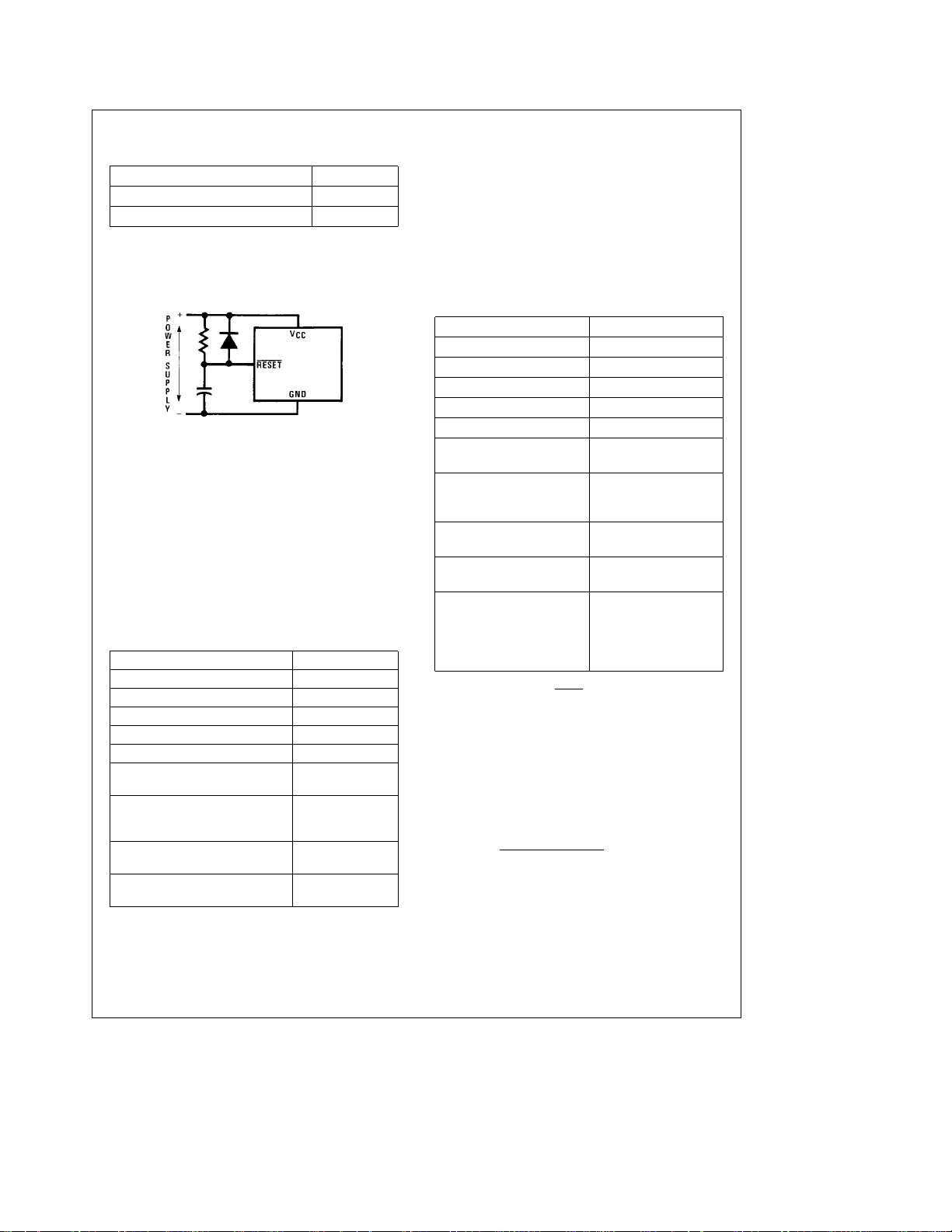
Reset
EXTERNAL RESET
The RESET input pin when pulled low initializes the microcontroller. The user must insure that the RESET pin is held
low until V
clock is stabilized. An R/C circuit with a delay 5x greater
than the power supply rise time is recommended
The device immediately goes into reset state when the
RESET input goes low. When the RESET pin goes high the
device comes out of reset state synchronously. The device
will be running within two instruction cycles of the RESET
pin going high. The following actions occur upon reset:
Port L TRI-STATE
Port G TRI-STATE
Port D HIGH
PC CLEARED
RAM Contents RANDOM with Power-On-
B, X, SP Same as RAM
PSW, CNTRL1, CNTRL2
and WDREG Reg. CLEARED
Multi-Input Wakeup Reg.
WKEDG, WKEN CLEARED
WKPND UNKNOWN
Data and Configuration
Registers forL&G CLEARED
WATCHDOG Timer Prescaler/Counter each
The device comes out of the HALT mode when the RESET
pin is pulled low. In this case, the user has to ensure that the
RESET signal is low long enough to allow the oscillator to
restart. An internal 256 t
tion with the two pin crystal oscillator. When the device
comes out of the HALT mode through Multi-Input Wakeup,
this delay allows the oscillator to stabilize.
The following additional actions occur after the device
comes out of the HALT mode through the RESET pin.
If a two pin crystal/resonator oscillator is being used:
RAM Contents UNCHANGED
Timer T1 and A Contents UNKNOWN
WATCHDOG Timer Prescaler/Counter ALTERED
is within the specified voltage range and the
CC
(Figure 4)
Reset
UNAFFECTED with external
Reset (power already applied)
loaded with FF
delay is normally used in conjunc-
c
.
http://www.national.com7
Functional Description (Continued)
If the external or RC Clock option is being used:
RAM Contents UNCHANGED
Timer T1 and A Contents UNCHANGED
WATCHDOG Timer Prescaler/Counter ALTERED
The external RESET takes priority over the Brown Out Reset.
Note: If the RESET pin is pulled low while Brown Out occurs (Brown Out
circuit has detected Brown Out condition), the external reset will not
occur until the Brown Out condition is removed. External reset has
priority only if V
RCl5cPower Supply Rise Time TL/DD/11208– 6
FIGURE 4. Recommended Reset Circuit
WATCHDOG RESET
With WATCHDOG enabled, the WATCHDOG logic resets
the device if the user program does not service the WATCHDOG timer within the selected service window. The
WATCHDOG reset does not disable the WATCHDOG.
Upon WATCHDOG reset, the WATCHDOG Prescaler/
Counter are each initialized with FF Hex.
The following actions occur upon WATCHDOG reset that
are different from external reset.
WDREN WATCHDOG Reset Enable bit UNCHANGED
WDUDF WATCHDOG Underflow bit UNCHANGED
Additional initialization actions that occur as a result of
WATCHDOG reset are as follows:
Port L TRI-STATE
Port G TRI-STATE
Port D HIGH
PC CLEARED
Ram Contents UNCHANGED
B, X, SP UNCHANGED
PSW, CNTRL1 and CNTRL2 (except
WDUDF Bit) Registers CLEARED
Multi-Input Wakeup Registers
WKEDG, WKEN CLEARED
WKPND UNKNOWN
Data and Configuration
Registers forL&G CLEARED
WATCHDOG Timer Prescalar/Counter
BROWN OUT RESET
The on-board Brown Out protection circuit resets the device
when the operating voltage (V
Out voltage. The device is held in reset when V
below the Brown Out Voltage. The device will remain in
is greater than the Brown Out voltage.
CC
each loaded with FF
) is lower than the Brown
CC
CC
stays
RESET as long as V
Device will resume execution if V
Out Voltage. If a two pin crystal/resonator clock option is
is below the Brown Out Voltage. The
CC
rises above the Brown
CC
selected, the Brown Out reset will trigger a 256tc delay. This
delay allows the oscillator to stabilize before the device exits the reset state. The delay is not used if the clock option is
either R/C or external clock. The contents of data registers
and RAM are unknown following a Brown Out reset. The
external reset takes priority over Brown Out Reset and will
deactivate the 256 tc cycles delay if in progress. The Brown
Out reset takes priority over the WATCHDOG reset.
The following actions occur as a result of Brown Out reset:
Port L TRI-STATE
Port G TRI-STATE
Port D HIGH
PC CLEARED
RAM Contents RANDOM
B, X, SP UNKNOWN
PSW, CNTRL1, CNTRL2
and WDREG Registers CLEARED
Multi-Input Wakeup Registers
WKEDG, WKEN CLEARED
WKPND UNKNOWN
Data and Configuration
Registers forL&G CLEARED
WATCHDOG Timer Prescalar/Counter each
loaded with FF
Timer T1 and Accumulator Unknown data after
coming out of the HALT
(through Brown Out
Reset) with any Clock
option
Note: The development system will detect the BROWN OUT RESET exter-
nally and will force the RESET
does not emulate the 256tc delay.
pin low. The Development System
Brown Out Detection
An on-board detection circuit monitors the operating voltage
(V
) and compares it with the minimum operating voltage
CC
specified. The Brown Out circuit is designed to reset the
device if the operating voltage is below the Brown Out voltage (between 1.8V to 4.2V at
b
40§Ctoa85§C). The Minimum operating voltage for the device is 2.5V with Brown
Out disabled, but with BROWN OUT enabled the device is
guaranteed to operate properly down to minimum Brown
Out voltage (Max frequency 4 MHz
of 0
Cto70§C the Brown Out voltage is expected to be
§
between 1.9V to 3.9V. The circuit can be enabled or dis-
), For temperature range
abled by Brown Out mask option. If the device is intended to
operate at lower V
max), the Brown Out circuit should be disabled by the mask
(lower than Brown Out voltage VBO
CC
option.
The Brown Out circuit may be used as a power-up reset
provided the power supply rise time is slower than 50 ms (0V
to 6.0V).
Note: Brown Out Circuit is active in HALT mode (with the Brown Out mask
option selected).
http://www.national.com 8
Functional Description (Continued)
Oscillator Circuits
EXTERNAL OSCILLATOR
CKI can be driven by an external clock signal provided it
meets the specified duty cycle, rise and fall times, and input
levels. CKO is available as a general purpose input G7
and/or Halt control.
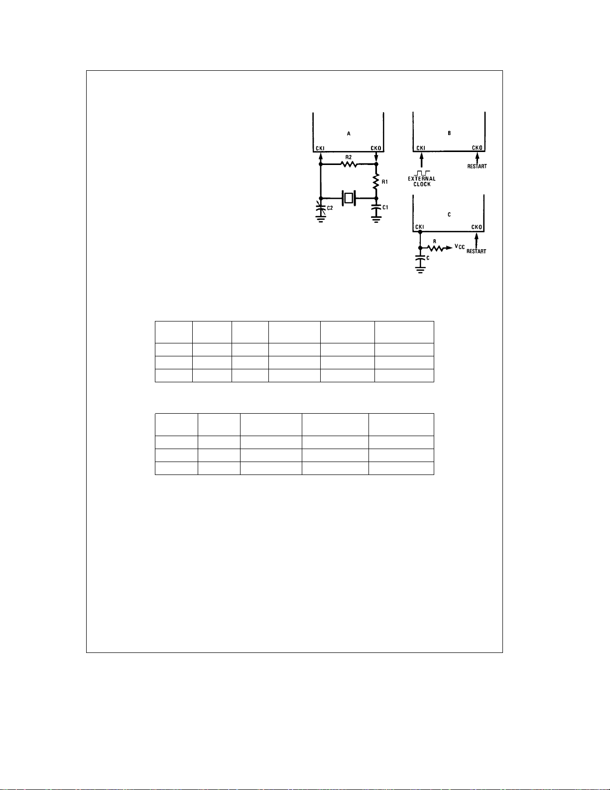
CRYSTAL OSCILLATOR
By selecting CKO as a clock output, CKI and CKO can be
connected to create a crystal controlled oscillator. Table I
shows the component values required for various standard
crystal values.
R/C OSCILLATOR
By selecting CKI as a single pin oscillator, CKI can make a
R/C oscillator. CKO is available as a general purpose input
and/or HALT control. Table II shows variation in the oscillator frequencies as functions of the component (R and C)
values.
FIGURE 5. Clock Oscillator Configurations
TABLE I. Crystal Oscillator Configuration
R1 R2 C1 C2 CKI Freq.
(kX)(MX) (pF) (pF) (MHz)
0 1 30 30– 36 10 V
0 1 30 30– 36 4 V
5.6 1 100 100 –156 0.455 V
TABLE II. RC Oscillator Configuration (Part-To-Part Variation)
R C CK1 Freq. Instr. Cycle
(kX) (pF) (MHz) (ms)
3.3 82 2.2 to 2.7 3.7 to 4.6 V
5.6 100 1.1 to 1.3 7.4 to 9.0 V
6.8 100 0.9 to 1.1 8.8 to 10.8 V
Conditions
e
CC
e
CC
e
CC
Conditions
e
5V
CC
e
5V
CC
e
5V
CC
TL/DD/11208– 7
5V
5V
5V
http://www.national.com9

Functional Description (Continued)
Halt Mode
The device is a fully static device. The device enters the
HALT mode by writing a one to the G7 bit of the G data
register. Once in the HALT mode, the internal circuitry does
not receive any clock signal and is therefore frozen in the
exact state it was in when halted. In this mode the chip will
only draw leakage current (output current and DC current
due to the Brown Out circuit if Brown Out is enabled).
The device supports four different methods of exiting the
HALT mode. The first method is with a low to high transition
on the CKO (G7) pin. This method precludes the use of the
crystal clock configuration (since CKO is a dedicated output). It may be used either with an RC clock configuration or
an external clock configuration. The second method of exiting the HALT mode is with the multi-Input Wakeup feature
on the L port. The third method of exiting the HALT mode is
by pulling the RESET input low. The fourth method is with
the operating voltage going below Brown Out voltage (if
Brown Out is enabled by mask option).
If the two pin crystal/resonator oscillator is being used and
Multi-Input Wakeup or Brown Out causes the device to exit
the HALT mode, the WAKEUP signal does not allow the
chip to start running immediately since crystal oscillators
have a delayed start up time to reach full amplitude and
freuqency stability. The WATCHDOG timer (consisting of an
8-bit prescaler followed by an 8-bit counter) is used to generate a fixed delay of 256tc to ensure that the oscillator has
indeed stabilized before allowing instruction execution. In
this case, upon detecting a valid WAKEUP signal only the
oscillator circuitry is enabled. The WATCHDOG Counter and
Prescaler are each loaded with a value of FF Hex. The
WATCHDOG prescaler is clocked with the tc instruction cycle. (The tc clock is derived by dividing the oscillator clock
down by a factor of 10). The Schmitt trigger following the
CKI inverter on the chip ensures that the WATCHDOG timer
is clocked only when the oscillator has a sufficiently large
amplitude to meet the Schmitt trigger specs. This Schmitt
trigger is not part of the oscillator closed loop. The start-up
timeout from the WATCHDOG timer enables the clock signals to be routed to the rest of the chip. The delay is not
activated when the device comes out of HALT mode
through RESET pin. Also, if the clock option is either RC or
External clock, the delay is not used, but the WATCHDOG
Prescaler/-Counter contents are changed. The Development System will not emulate the 256tc delay.
The RESET
pin or Brown Out will cause the device to reset
and start executing from address X’0000. A low to high transition on the G7 pin (if single pin oscillator is used) or MultiInput Wakeup will cause the device to start executing from
the address following the HALT instruction.
When RESET
pin is used to exit the device from the HALT
mode and the two pin crystal/resonator (CKI/CKO) clock
option is selected, the contents of the Accumulator and the
Timer T1 are undetermined following the reset. All other
information except the WATCHDOG Prescaler/Counter
contents is retained until continuing. If the device comes out
of the HALT mode through Brown Out reset, the contents of
data registers and RAM are unknown following the reset. All
information except the WATCHDOG Prescaler/Counter
contents is retained if the device exits the HALT mode
through G7 pin or Multi-Input Wakeup.
G7 is the HALT-restart pin, but it can still be used as an
input. If the device is not halted, G7 can be used as a general purpose input.
If the Brown Out Enable mask option is selected, the Brown
Out circuit remains active during the HALT mode causing
additional current to be drawn.
Note: To allow clock resynchronization, it is necessary to program two
NOP’s immediately after the device comes out of the HALT mode.
The user must program two NOP’s following the ‘‘enter HALT mode’’
(set G7 data bit) instruction.
http://www.national.com 10
 Loading...