

查询COP472-3供应商
COP472-3 Liquid Crystal Display Controller
COP472-3 Liquid Crystal Display Controller
July 1995
General Description
The COP472 –3 Liquid Crystal Display (LCD) Controller is a
peripheral member of the COPS
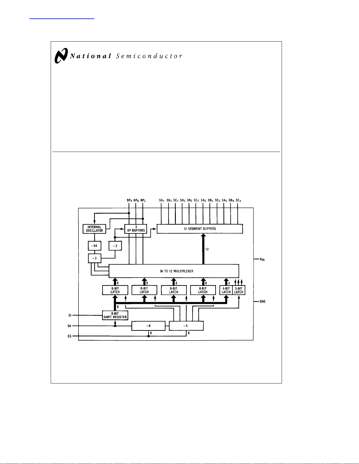
CMOS technology. The COP472-3 drives a multiplexed liquid crystal display directly. Data is loaded serially and is held
in internal latches. The COP472-3 contains an on-chip oscillator and generates all the multi-level waveforms for backplanes and segment outputs on a triplex display. One
COP472-3 can drive 36 segments multiplexed as3x12
(4(/2 digit display). Two COP472-3 devices can be used together to drive 72 segments (3 x 24) which could be an 8(/2
digit display.
TM
family, fabricated using
Block Diagram
Features
Y
Direct interface to TRIPLEX LCD
Y
Low power dissipation (100 mW typ.)
Y
Low cost
Y
Compatible with all COPS processors
Y
Needs no refresh from processor
Y
On-chip oscillator and latches
Y
Expandable to longer displays
Y
Operates from display voltage
Y
MICROWIRETMcompatible serial I/O
Y
20-pin Dual-In-Line package and 20-pin SO
COPSTMand MICROWIRETMare trademarks of National Semiconductor Corporation.
C
1996 National Semiconductor Corporation RRD-B30M56/Printed in U. S. A.
TL/DD/6932
TL/DD/6932– 1
http://www.national.com
Absolute Maximum Ratings
Voltage at CS, DI, SK pins
Voltage at all other Pins
Operating Temperature Range 0§Cto70§C
b
b
0.3V to V
0.3V toa9.5V
a
0.3V
DD
Storage Temperature
b
65§Ctoa150§C
Lead Temp. (Soldering, 10 Seconds) 300§C
DC Electrical Characteristics
GNDe0V, V
DD
e
3.0V to 5.5V, T
Parameter Conditions Min Max Units
Power Supply Voltage, V
DD
Power Supply Current, IDD(Note 1) V
Input Levels
DI, SK, CS
V
IL
V
IH
BPA (as Osc. in)
V
IL
V
IH
Output Levels, BPC (as Osc. Out)
V
OL
V
OH
Backplane Outputs (BPA, BPB, BPC)
V
BPA, BPB, BPC
V
BPA, BPB, BPC
V
BPA, BPB, BPC
V
BPA, BPB, BPC
Segment Outputs (SA
V
SEG
V
SEG
V
SEG
V
SEG
ON During V
OFF BPaTime (/3 V
ON During 0 DV Volts
OFF BPbTime )/3 V
E
ON During 0 DV Volts
1
OFF BPaTime )/3 V
ON During V
OFF BPbTime (/3 V
Internal Oscillator Frequency 15 80 kHz
Frame Time (Int. Osc.d192) 2.4 12.8 ms
Scan Frequency (1/T
SCAN
SK Clock Frequency 4 250 kHz
SK Width 1.7 ms
DI
Data Setup, t
Data Hold, t
SETUP
HOLD
CS
t
SETUP
t
HOLD
Output Loading Capacitance 100 pF
Note 1: Power supply current is measured in stand-alone mode with all outputs open and all inputs at V
Note 2: DVe0.05VDD.
e
0§Cto70§C (depends on display characteristics)
A
3.0 5.5 Volts
e
5.5V 250 mA
DD
e
V
3V 100 mA
DD
0.8 Volts
0.7 V
DD
9.5 Volts
0.6 Volts
b
V
0.6 V
DD
DD
0.4 Volts
b
V
0.4 V
SA
DD
b
DVVDDVolts
DD
b
DV (/3 V
DD
b
DV )/3 V
DD
)
4
b
DV )/3 V
DD
b
DVVDDVolts
DD
b
DV (/3 V
DD
DD
a
DV Volts
DD
a
DV Volts
DD
a
DV Volts
DD
a
DV Volts
DD
) 39 208 Hz
1.0 ms
100 ns
1.0 ms
1.0 ms
.
DD
Volts
Volts
http://www.national.com 2
Absolute Maximum Ratings
If Military/Aerospace specified devices are required,
please contact the National Semiconductor Sales
Office/Distributors for availability and specifications.
Voltage at CS, DI, SK Pins
Voltage at All Other Pins
Operating Temperature Range
b
0.3V toa9.5V
b
0.3V to V
b
40§Ctoa85§C
DD
a
0.3V
Storage Temperature
b
65§Ctoa150§C
Lead Temperature
(Soldering, 10 seconds) 300§C
DC Electrical Characteristics
GNDe0V, V
DD
e
3.0V to 5.5V, T
Parameter Conditions Min Max Units
Power Supply Voltage, V
DD
Power Supply Current, IDD(Note 1) V
Input Levels
DI, SK, CS
V
IL
V
IH
BPA (as Osc. In)
V
IL
V
IH
Output Levels, BPC (as Osc. Out)
V
OL
V
OH
Backplane Outputs (BPA, BPB, BPC)
V
BPA, BPB, BPC
V
BPA, BPB, BPC
V
BPA, BPB, BPC
V
BPA, BPB, BPC
Segment Outputs (SA
V
SEG
V
SEG
V
SEG
V
SEG
ON During V
OFF BPaTime (/3 V
ON During 0 DV Volts
OFF BPbTime )/3 V
E
ON During 0 DV Volts
1
OFF BPaTime )/3 V
ON During V
OFF BPbTime (/3 V
Internal Oscillator Frequency 15 80 kHz
Frame Time (Int. Osc.d192) 2.4 12.8 ms
Scan Frequency (1/T
SCAN
SK Clock Frequency 4 250 kHz
SK Width 1.7 ms
DI
Data Setup, t
Data Hold, t
SETUP
HOLD
CS
t
SETUP
t
HOLD
Output Loading Capacitance 100 pF
Note 1: Power supply current is measured in stand-alone mode with all outputs open and all inputs at VDD.
Note 2: DV
e
0.05 VDD.
eb
40§Ctoa85§C (depends on display characteristics)
A
3.0 5.5 Volts
e
5.5V 300 mA
DD
e
V
3V 120 mA
DD
0.8 Volts
0.7 V
DD
9.5 Volts
0.6 Volts
b
V
0.6 V
DD
DD
0.4 Volts
b
V
0.4 V
SA
DD
b
DVVDDVolts
DD
b
DV (/3 V
DD
b
DV )/3 V
DD
)
4
b
DV )/3 V
DD
b
DVVDDVolts
DD
b
DV (/3 V
DD
DD
a
DV Volts
DD
a
DV Volts
DD
a
DV Volts
DD
a
DV Volts
DD
) 39 208 Hz
1.0 ms
100 ns
1.0 ms
1.0 ms
Volts
Volts
http://www.national.com3

Dual-In-Line Package
Top View
TL/DD/6932– 2
Order Number COP472MW-3 or COP472N-3
See NS Package Number M20A or N20A
FIGURE 2. Connection Diagram
Pin Description
CS
V
DD
GND Ground
Chip select
Power supply (display voltage)
DI Serial data input
SK Serial clock input
BP
A
BP
B
BP
C
SA1ESC4 12 multiplexed outputs
Display backplane A (or oscillator in)
Display backplane B
Display backplane C (or oscillator out)
FIGURE 3. Serial Load Timing Diagram
FIGURE 4. Backplane and Segment Waveforms
FIGURE 5. Typical Display Internal Connections
Epson LD-370
TL/DD/6932– 3
TL/DD/6932– 4
TL/DD/6932– 5
http://www.national.com 4

Functional Description
The COP472-3 drives 36 bits of display information organized as twelve segments and three backplanes. The
COP472-3 requires 40 information bits: 36 data and 4 control. The function of each control bit is described below.
Display information format is a function of the LCD interconnections. A typical segment/backplane configuration is illustrated in
Figure 5
drive 4 digits of 9 segments.
To adapt the COP472-3 to any LCD display configuration,
the segment/backplane multiplex scheme is illustrated in
Table I.
Two or more COP472-3 chips can be cascaded to drive
additional segments. There is no limit to the number of
COP472-3’s that can be used as long as the output loading
capacitance does not exceed specification.
Bit Number
10 SB2, BPB SG
11 SC2, BPA SF
12 SC2, BPB SE
13 SB2, BPC SD
14 SA2, BPB SC
15 SA2, BPA SB
16 SB2, BPA SA
17 SA3, BPC SH
18 SB3, BPB SG
19 SC3, BPA SF
20 SC3, BPB SE
21 SB3, BPC SD
22 SA3, BPB SC
23 SA3, BPA SB
24 SB3, BPA SA
25 SA4, BPC SH
26 SB4, BPB SG
27 SC4, BPA SF
28 SC4, BPB SE
29 SB4, BPC SD
30 SA4, BPB SC
31 SA4, BPA SB
32 SB4, BPA SA
33 SC1, BPC SPA Digit 1
34 SC2, BPC SP2 Digit 2
35 SC3, BPC SP3 Digit 3
36 SC4, BPC SP4 Digit 4
37 not used
38 Q6
39 Q7
40 SYNC
, with this configuration the COP472-3 will
TABLE I. COP472-3 Segment/Backplane
Multiplex Scheme
Segment, Data to
Backplane Numeric Display
1 SA1, BPC SH
2 SB1, BPB SG
3 SC1, BPA SF
4 SC1, BPB SE
5 SB1, BPC SD
6 SA1, BPB SC
7 SA1, BPA SB
8 SB1, BPA SA
9 SA2, BPC SH
Digit 1
Digit 2
Digit 3
Digit 4
SEGMENT DATA BITS
Data is loaded in serially, in sets of eight bits. Each set of
segment data is in the following format:
SA SB SC SD SE SF SG SH
Data is shifted into an eight bit shift register. The first bit of
the data is for segment H, digit 1. The eighth bit is segment
A, digit 1. A set of eight bits is shifted in and then loaded into
the digit one latches. The second set of 8 bits is loaded into
digit two latches. The third set into digit three latches, and
the fourth set is loaded into digit four latches.
CONTROL BITS
The fifth set of 8 data bits contains special segment data
and control data in the following format:
SYNC Q7 Q6 X SP4 SP3 SP2 SP1
The first four bits shifted in contain the special character
segment data. The fifth bit is not used. The sixth and seventh bits program the COP472-3 as a stand alone LCD driver or as a master or slave for cascading COP472-3’s. BPC
of the master is connected to BPA of each slave. The following table summarizes the function of bits six and seven:
Q7 Q6 Function BPC Output BPA Output
1 1 Slave Backplane Oscillator
Output Input
0 1 Stand Alone Backplane Backplane
Output Output
1 0 Not Used Internal Oscillator
Osc. Output Input
0 0 Master Internal Backplane
Osc. Output Output
The eighth bit is used to synchronize two COP472-3’s to
drive an 8(/2-digit display.
http://www.national.com5

LOADING SEQUENCE TO DRIVE A 4(/2-DIGIT DISPLAY
Steps:
1. Turn CE
low.
2. Clock in 8 bits of data for digit 1.
3. Clock in 8 bits of data for digit 2.
4. Clock in 8 bits of data for digit 3.
5. Clock in 8 bits of data for digit 4.
6. Clock in 8 bits of data for special segment and control
function of BPC and BPA.
0011SP4SP3SP2SP1
7. Turn CS high.
Note: CS may be turned high after any step. For example to
load only 2 digits of data, do steps 1, 2, 3, and 7.
CS
must make a high to low transition before loading data in
order to reset internal counters.
LOADING SEQUENCE TO DRIVE AN
8(/2-DIGIT DISPLAY
Two or more COP472-3’s may be connected together to
drive additional segments. An eight digit multiplexed display
is shown in
Figure 7
. The following is the loading sequence
to drive an eight digit display using two COP472-3’s. The
right chip is the master and the left the slave.
Steps:
1. Turn CS
low on both COP472-3’s.
2. Shift in 32 bits of data for the slave’s four digits.
3. Shift in 4 bits of special segment data: a zero and three
ones.
1110SP4SP3SP2SP1
This synchronizes both the chips and BPA is oscillator
input. Both chips are now stopped.
4. Turn CS high to both chips.
5. Turn CS low to master COP472-3.
6. Shift in 32 bits of data for the master’s 4 digits.
7. Shift in four bits of special segment data, a one and
three zeros.
0001SP4SP3SP2SP1
This sets the master COP472-3 to BPA as a normal
backplane output and BPC as oscillator output. Now
both the chips start and run off the same oscillator.
8. Turn CS
high.
The chips are now synchronized and driving 8 digits of display. To load new data simply load each chip separately in
the normal manner, keeping the correct status bits to each
COP472-3 (0110 or 0001).
FIGURE 6. System Diagram – 4(/2 Digit Display
TL/DD/6932– 6
TL/DD/6932– 7
FIGURE 7. System Diagram – 8(/2 Digit Display
http://www.national.com 6

Physical Dimensions inches (millimeters) unless otherwise noted
20-Lead Molded DIP (M)
Order Number COP472MW-3
NS Package Number M20B
http://www.national.com7

Physical Dimensions inches (millimeters) unless otherwise noted (Continued)
20-Lead Molded DIP (N)
Order Number COP472N-3
COP472-3 Liquid Crystal Display Controller
NS Package Number N20A
LIFE SUPPORT POLICY
NATIONAL’S PRODUCTS ARE NOT AUTHORIZED FOR USE AS CRITICAL COMPONENTS IN LIFE SUPPORT
DEVICES OR SYSTEMS WITHOUT THE EXPRESS WRITTEN APPROVAL OF THE PRESIDENT OF NATIONAL
SEMICONDUCTOR CORPORATION. As used herein:
1. Life support devices or systems are devices or 2. A critical component is any component of a life
systems which, (a) are intended for surgical implant support device or system whose failure to perform can
into the body, or (b) support or sustain life, and whose be reasonably expected to cause the failure of the life
failure to perform, when properly used in accordance support device or system, or to affect its safety or
with instructions for use provided in the labeling, can effectiveness.
be reasonably expected to result in a significant injury
to the user.
National Semiconductor National Semiconductor National Semiconductor National Semiconductor
Corporation Europe Hong Kong Ltd. Japan Ltd.
1111 West Bardin Road Fax:
Arlington, TX 76017 Email: europe.support@nsc.com Ocean Centre, 5 Canton Rd. Fax: 81-043-299-2408
Tel: 1(800) 272-9959 Deutsch Tel:
Fax: 1(800) 737-7018 English Tel:
http://www.national.com
National does not assume any responsibility for use of any circuitry described, no circuit patent licenses are implied and National reserves the right at any time without notice to change said circuitry and specifications.
Fran3ais Tel:
Italiano Tel:a49 (0) 180-534 16 80 Fax: (852) 2736-9960
a
49 (0) 180-530 85 86 13th Floor, Straight Block, Tel: 81-043-299-2308
a
49 (0) 180-530 85 85 Tsimshatsui, Kowloon
a
49 (0) 180-532 78 32 Hong Kong
a
49 (0) 180-532 93 58 Tel: (852) 2737-1600
 Loading...