

Page 1
CD4020BM/CD4020BC
14-Stage Ripple Carry Binary Counters
CD4040BM/CD4040BC
12-Stage Ripple Carry Binary Counters
CD4060BM/CD4060BC
14-Stage Ripple Carry Binary Counters
February 1988
CD4020BM/BC 14-Stage Ripple Carry Binary Counters/CD4040BM/BC 12-Stage
Ripple Carry Binary Counters CD4060BM/BC 14-Stage Ripple Carry Binary Counters
General Description
The CD4020BM/CD4020BC, CD4060BM/CD4060BC are
14-stage ripple carry binary counters, and the CD4040BM/
CD4040BC is a 12-stage ripple carry binary counter. The
counters are advanced one count on the negative transition
of each clock pulse. The counters are reset to the zero state
by a logical ‘‘1’’ at the reset input independent of clock.
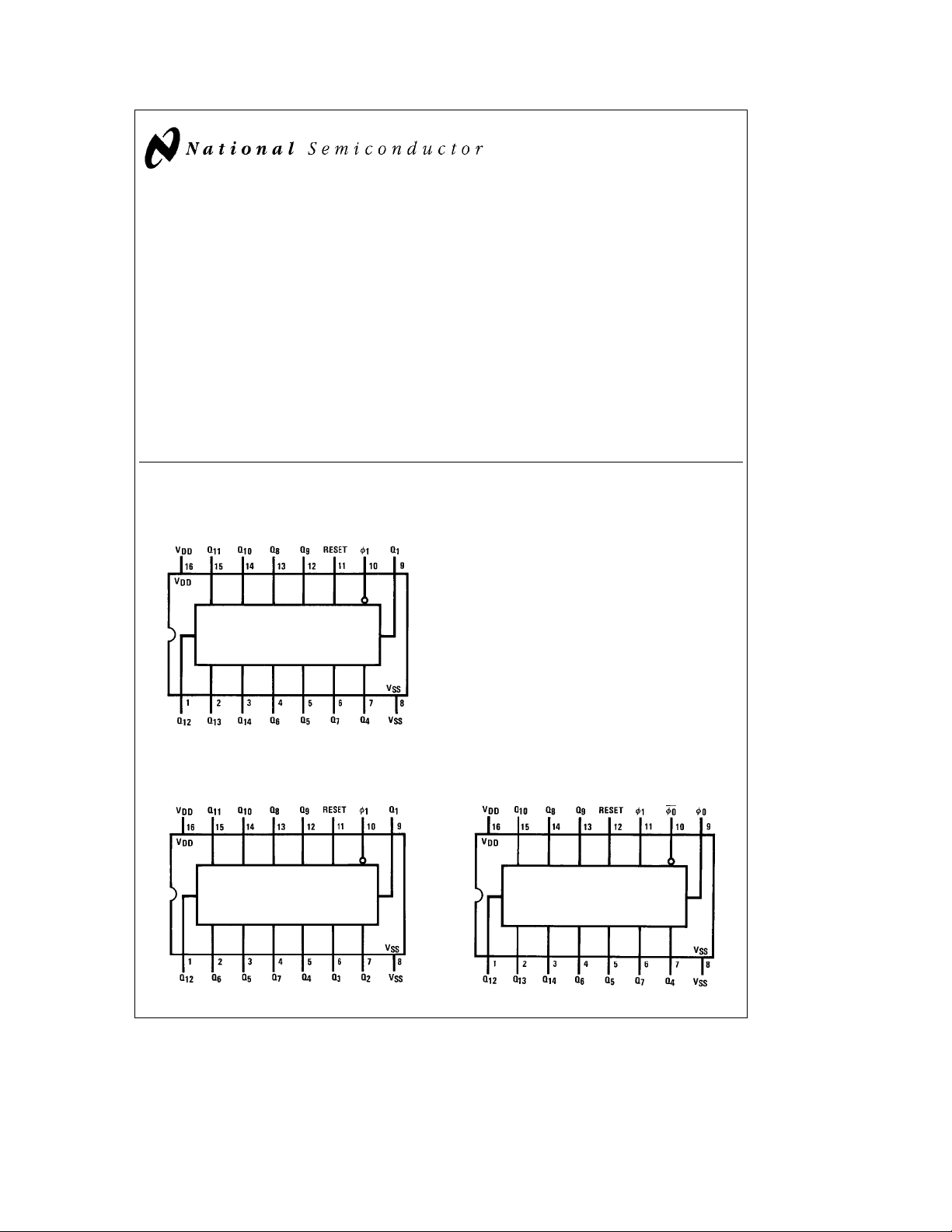
Connection Diagrams
Dual-In-Line Package
CD4020BM/CD4020BC
TL/F/5953– 1
Top View
Dual-In-Line Package
CD4040BM/CD4040BC
Features
Y
Wide supply voltage range 1.0V to 15V
Y
High noise immunity 0.45 VDD(typ.)
Y
Low power TTL Fan out of 2 driving 74L
compatibility or 1 driving 74LS
Y
Medium speed operation 8 MHz typ. at V
Y
Schmitt trigger clock input
Order Number CD4020B, CD4040B or CD4060B
Dual-In-Line Package
CD4060BM/CD4060BC
DD
e
10V
Top View
C
1995 National Semiconductor Corporation RRD-B30M105/Printed in U. S. A.
TL/F/5953
TL/F/5953– 2
Top View
TL/F/5953– 3
Page 2
Absolute Maximum Ratings (Notes 1 and 2)
If Military/Aerospace specified devices are required,
please contact the National Semiconductor Sales
Office/Distributors for availability and specifications.
Supply Voltage (V
DD
)
Input Voltage (VIN)
Storage Temperature Range (T
)
S
b
0.5V toa18V
b
0.5V to V
b
65§Ctoa150§C
DD
a
0.5V
Recommended Operating
Conditions
Supply Voltage (VDD)
Input Voltage (VIN) 0VtoV
Operating Temperature Range (TA)
CD40XXBM
CD40XXBC
a
3V toa15V
b
55§Ctoa125§C
b
40§Ctoa85§C
Package Dissipation (PD)
Dual-In-Line 700 mW
Small Outline 500 mW
Lead Temperature (T
(Soldering, 10 seconds) 260
)
L
C
§
DC Electrical Characteristics CD40XXBM (Note 2)
b
Symbol Parameter Conditions
55§C
Min Max Min Typ Max Min Max
I
Quiescent Device Current V
DD
V
Low Level Output Voltage V
OL
V
High Level Output Voltage V
OH
V
Low Level Input Voltage V
IL
V
High Level Input Voltage V
IH
I
Low Level Output Current V
OL
(See Note 3) V
I
High Level Output Current V
OH
(See Note 3) V
I
Input Current V
IN
Note 1: ‘‘Absolute Maximum Ratings’’ are those values beyond which the safety of the device cannot be guaranteed. They are not meant to imply that the devices
should be operated at these limits. The tables of ‘‘Recommended Operating Conditions’’ and ‘‘Electrical Characteristics’’ provide conditions for actual device
operation.
Note 2: V
Note 3: Data does not apply to oscillator points w
e
0V unless otherwise specified.
SS
e
DD
e
V
DD
e
V
DD
e
DD
e
V
DD
e
V
DD
e
DD
e
V
DD
e
V
DD
e
DD
e
V
DD
e
V
DD
e
DD
e
V
DD
e
V
DD
e
DD
e
DD
e
V
DD
e
DD
e
DD
e
V
DD
e
DD
e
V
DD
0
e
5V, V
10V, V
15V, V
IN
IN
IN
VDDor V
e
VDDor V
e
VDDor V
SS
SS
SS
5 5 150 mA
10 10 300 mA
20 20 600 mA
5V 0.05 0 0.05 0.05 V
10V 0.05 0 0.05 0.05 V
15V 0.05 0 0.05 0.05 V
5V 4.95 4.95 5 4.95 V
10V 9.95 9.95 10 9.95 V
15V 14.95 14.95 15 14.95 V
e
5V, V
10V, V
15V, V
5V, V
10V, V
15V, V
5V, V
10V, V
15V, V
5V, V
10V, V
15V, V
15V, V
15V, V
and w
0.5V or 4.5V 1.5 2 1.5 1.5 V
O
e
1.0V or 9.0V 3.0 4 3.0 3.0 V
O
e
1.5V or 13.5V 4.0 6 4.0 4.0 V
O
e
0.5V or 4.5V 3.5 3.5 3 3.5 V
O
e
1.0V or 9.0V 7.0 7.0 6 7.0 V
O
e
1.5V or 13.5V 11.0 11.0 9 11.0 V
O
e
0.4V 0.64 0.51 0.88 0.36 mA
O
e
0.5V 1.6 1.3 2.25 0.9 mA
O
e
1.5V 4.2 3.4 8.8 2.4 mA
O
e
4.6V
O
e
9.5V
O
e
13.5V
O
e
0V
IN
e
15V 0.10 10
IN
of CD4060BM/CD4060BC. IOHand IOLare tested one output at a time.
0
b
0.64
b
1.6
b
4.2
b
0.10
b
0.51b0.88
b
1.3b2.25
b
3.4b8.8
b
a
25§C
b
5
b
10
0.10
b
5
0.10 1.0 mA
a
125§C
b
0.36 mA
b
0.9 mA
b
2.4 mA
b
1.0 mA
DD
Units
DC Electrical Characteristics 40XXBC (Note 2)
Symbol Parameter Conditions
I
DD
V
OL
Quiescent Device Current V
Low Level Output Voltage V
e
DD
e
V
DD
e
V
DD
e
DD
e
V
DD
e
V
DD
e
5V, V
10V, V
15V, V
IN
e
IN
e
IN
VDDor V
VDDor V
VDDor V
5V 0.05 0 0.05 0.05 V
10V 0.05 0 0.05 0.05 V
15V 0.05 0 0.05 0.05 V
b
40§C
a
25§C
a
85§C
Units
Min Max Min Typ Max Min Max
SS
SS
SS
20 20 150 mA
40 40 300 mA
80 80 600 mA
2
Page 3

DC Electrical Characteristics 40XXBC (Note 2) (Continued)
b
Symbol Parameter Conditions
40§C
Min Max Min Typ Max Min Max
e
e
5V 4.95 4.95 5 4.95 V
DD
e
V
10V 9.95 9.95 10 9.95 V
DD
e
V
15V 14.95 14.95 15 14.95 V
DD
DD
V
DD
V
DD
DD
V
DD
V
DD
DD
DD
V
DD
DD
DD
V
DD
DD
V
DD
200k, t
e
e
e
e
e
e
e
e
e
e
e
e
e
e
r
e
5V, V
10V, V
15V, V
5V, V
10V, V
15V, V
5V, V
10V, V
15V, V
5V, V
10V, V
15V, V
15V, V
15V, V
e
0.5V or 4.5V 1.5 2 1.5 1.5 V
O
e
1.0V or 9.0V 3.0 4 3.0 3.0 V
O
e
1.5V or 13.5V 4.0 6 4.0 4.0 V
O
e
0.5V or 4.5V 3.5 3.5 3 3.5 V
O
e
1.0V or 9.0V 7.0 7.0 6 7.0 V
O
e
1.5V or 13.5V 11.0 11.0 9 11.0 V
O
e
0.4V 0.52 0.44 0.88 0.36 mA
O
e
0.5V 1.3 1.1 2.25 0.9 mA
O
e
1.5V 3.6 3.0 8.8 2.4 mA
O
e
4.6V
O
e
9.5V
O
e
13.5V
O
e
0V
IN
e
15V 0.30 10
IN
e
t
20 ns, unless otherwise noted
f
b
0.52
b
1.3
b
3.6
b
0.30
V
High Level Output Voltage V
OH
V
Low Level Input Voltage V
IL
V
High Level Input Voltage V
IH
I
Low Level Output Current V
OL
(See Note 3) V
I
High Level Output Current V
OH
(See Note 3) V
I
Input Current V
IN
AC Electrical Characteristics* CD4020BM/CD4020BC, CD4040BM/CD4040BC
e
T
A
25§C, C
L
e
50 pF, R
L
Symbol Parameter Conditions Min Typ Max Units
t
PHL1,tPLH1
t
PHL,tPLH
t
THL,tTLH
tWL,t
WH
t
rCL,tfCL
f
CL
t
PHL(R)
t
WH(R)
C
in
C
pd
*AC Parameters are guaranteed by DC correlated testing.
Propagation Delay Time to Q
Interstage Propagation Delay Time V
from Q
to Q
n
na1
Transition Time V
Minimum Clock Pulse Width V
Maximum Clock Rise and Fall Time V
Maximum Clock Frequency V
Reset Propagation Delay V
Minimum Reset Pulse Width V
Average Input Capacitance Any Input 5 7.5 pF
Power Dissipation Capacitance 50 pF
1
e
V
5V 250 550 ns
DD
e
V
10V 100 210 ns
DD
e
V
15V 75 150 ns
DD
e
5V 150 330 ns
DD
e
V
10V 60 125 ns
DD
e
V
15V 45 90 ns
DD
e
5V 100 200 ns
DD
e
V
10V 50 100 ns
DD
e
V
15V 40 80 ns
DD
e
5V 125 335 ns
DD
e
V
10V 50 125 ns
DD
e
V
15V 40 100 ns
DD
e
5V No Limit ns
DD
e
V
10V No Limit ns
DD
e
V
15V No Limit ns
DD
e
5V 1.5 4 MHz
DD
e
V
10V 4 10 MHz
DD
e
V
15V 5 12 MHz
DD
e
5V 200 450 ns
DD
e
V
10V 100 210 ns
DD
e
V
15V 80 170 ns
DD
e
5V 200 450 ns
DD
e
V
10V 100 210 ns
DD
e
V
15V 80 170 ns
DD
a
b
0.44b0.88
b
1.1b2.25
b
3.0b8.8
b
25§C
b
b
5
b
10
0.30
b
5
0.30 1.0 mA
a
0.36 mA
b
0.9 mA
b
2.4 mA
85§C
b
1.0 mA
Units
3
Page 4

AC Electrical Characteristics* CD4060BM/CD4060BC
e
T
25§C, C
A
L
e
50 pF, R
e
L
200k, t
e
e
t
r
20 ns, unless otherwise noted
f
Symbol Parameter Conditions Min Typ Max Units
t
PHL4,tPLH4
t
PHL,tPLH
t
THL,tTLH
tWL,t
WH
t
rCL,tfCL
f
CL
t
PHL(R)
t
WH(R)
C
in
C
pd
*AC Parameters are guaranteed by DC correlated testing.
Propagation Delay Time to Q
Interstage Propagation Delay Time V
from Q
to Q
n
na1
Transition Time V
Minimum Clock Pulse Width V
Maximum Clock Rise and Fall Time V
Maximum Clock Frequency V
Reset Propagation Delay V
Minimum Reset Pulse Width V
Average Input Capacitance Any Input 5 7.5 pF
Power Dissipation Capacitance 50 pF
4
e
V
5V 550 1300 ns
DD
e
V
10V 250 525 ns
DD
e
V
15V 200 400 ns
DD
e
5V 150 330 ns
DD
e
V
10V 60 125 ns
DD
e
V
15V 45 90 ns
DD
e
5V 100 200 ns
DD
e
V
10V 50 100 ns
DD
e
V
15V 40 80 ns
DD
e
5V 170 500 ns
DD
e
V
10V 65 170 ns
DD
e
V
15V 50 125 ns
DD
e
5V No Limit ns
DD
e
V
10V No Limit ns
DD
e
V
15V No Limit ns
DD
e
5V 1 3 MHz
DD
e
V
10V 3 8 MHz
DD
e
V
15V 4 10 MHz
DD
e
5V 200 450 ns
DD
e
V
10V 100 210 ns
DD
e
V
15V 80 170 ns
DD
e
5V 200 450 ns
DD
e
V
10V 100 210 ns
DD
e
V
15V 80 170 ns
DD
CD4060B Typical Oscillator Connections
RC Oscillator
TL/F/5953– 4
4
Crystal Oscillator
TL/F/5953– 5
Page 5

Schematic Diagrams
CD4020BM/CD4020BC Schematic Diagram
TL/F/5953– 6
CD4040BM/CD4040BC Schematic Diagram
CD4060BM/CD4060BC Schematic Diagram
5
TL/F/5953– 7
TL/F/5953– 8
Page 6

Physical Dimensions inches (millimeters)
Ceramic Dual-In-Line Package (J)
Order Number CD4020BMJ, CD4020BCJ,
CD4040BMJ, CD4040BCJ, CD4060BMJ or CD4060BCJ
NS Package Number J16A
Molded Dual-In-Line Package (N)
Order Number CD4020BMN, CD4020BCN,
CD4040BMN, CD4040BCN, CD4060BMN or CD4060BCN
NS Package Number N16E
LIFE SUPPORT POLICY
NATIONAL’S PRODUCTS ARE NOT AUTHORIZED FOR USE AS CRITICAL COMPONENTS IN LIFE SUPPORT
DEVICES OR SYSTEMS WITHOUT THE EXPRESS WRITTEN APPROVAL OF THE PRESIDENT OF NATIONAL
SEMICONDUCTOR CORPORATION. As used herein:
1. Life support devices or systems are devices or 2. A critical component is any component of a life
systems which, (a) are intended for surgical implant support device or system whose failure to perform can
CD4020BM/BC 14-Stage Ripple Carry Binary Counters/CD4040BM/BC 12-Stage
into the body, or (b) support or sustain life, and whose be reasonably expected to cause the failure of the life
failure to perform, when properly used in accordance support device or system, or to affect its safety or
with instructions for use provided in the labeling, can effectiveness.
be reasonably expected to result in a significant injury
Ripple Carry Binary Counters CD4060BM/BC 14-Stage Ripple Carry Binary Counters
to the user.
National Semiconductor National Semiconductor National Semiconductor National Semiconductor
Corporation Europe Hong Kong Ltd. Japan Ltd.
1111 West Bardin Road Fax: (
Arlington, TX 76017 Email: cnjwge@tevm2.nsc.com Ocean Centre, 5 Canton Rd. Fax: 81-043-299-2408
Tel: 1(800) 272-9959 Deutsch Tel: (
Fax: 1(800) 737-7018 English Tel: (
National does not assume any responsibility for use of any circuitry described, no circuit patent licenses are implied and National reserves the right at any time without notice to change said circuitry and specifications.
Fran3ais Tel: (
Italiano Tel: (
a
49) 0-180-530 85 86 13th Floor, Straight Block, Tel: 81-043-299-2309
a
49) 0-180-530 85 85 Tsimshatsui, Kowloon
a
49) 0-180-532 78 32 Hong Kong
a
49) 0-180-532 93 58 Tel: (852) 2737-1600
a
49) 0-180-534 16 80 Fax: (852) 2736-9960
 Loading...