

Page 1
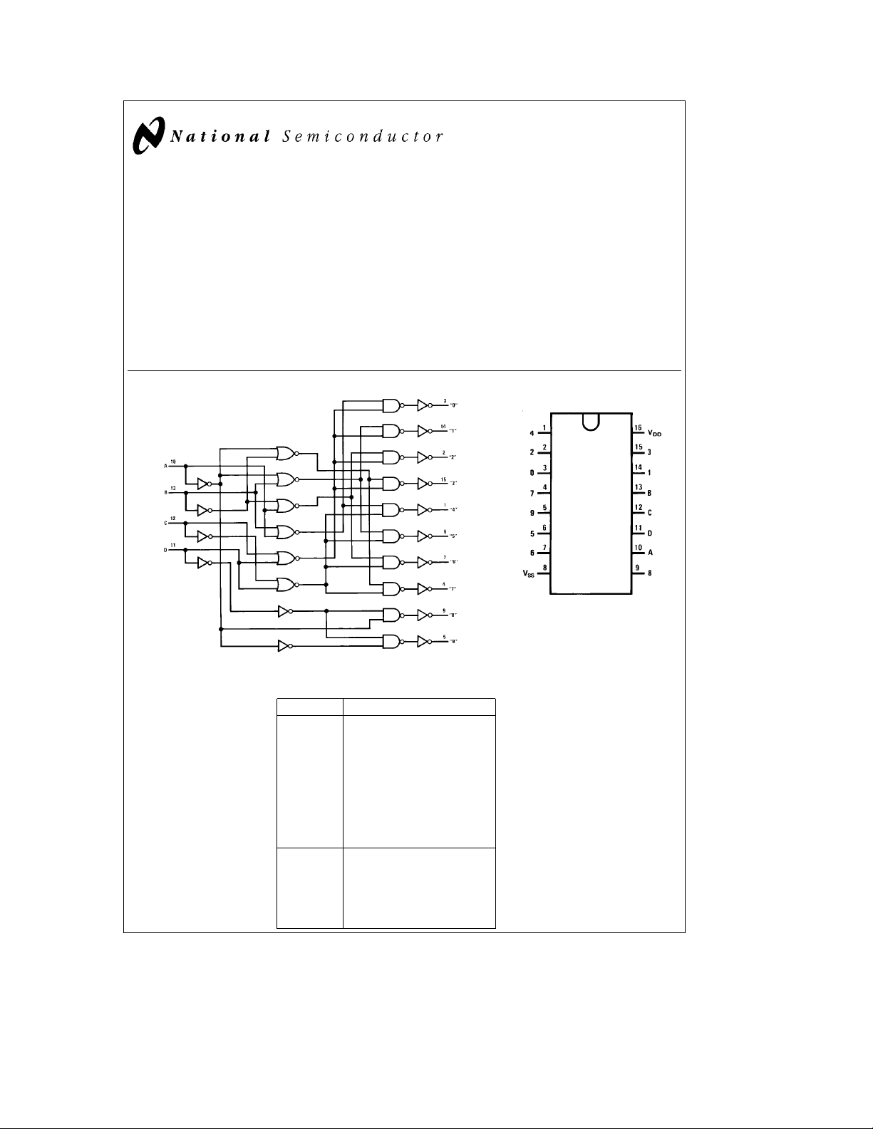
CD4028BM/CD4028BC BCD-to-Decimal Decoder
General Description
The CD4028BM/CD4028BC is a BCD-to-decimal or binaryto-octal decoder consisting of 4 inputs, decoding logic
gates, and 10 output buffers. A BCD code applied to the 4
inputs, A, B, C, and D, results in a high level at the selected
1-of-10 decimal decoded outputs. Similarly, a 3-bit binary
code applied to inputs A, B, and C is decoded in octal at
outputs 0 –7. A high level signal at the D input inhibits octal
decoding and causes outputs 0–7 to go low.
All inputs are protected against static discharge damage by
diode clamps to V
DD
and VSS.
Features
Y
Wide supply voltage range 3.0V to 15V
Y
High noise immunity 0.45 VDD(typ.)
Y
Low power TTL fan out of 2 driving 74L
compatibility or 1 driving 74LS
Y
Low power
Y
Glitch free outputs
Y
‘‘Positive logic’’ on inputs and outputs
Applications
Y
Code conversion
Y
Address decoding
Y
Indicator-tube decoder
CD4028BM/CD4028BC BCD-to-Decimal Decoder
February 1988
Logic and Connection Diagrams
Dual-In-Line Package
Top View
Order Number CD4028B
TL/F/5959– 1
TL/F/5959– 2
Truth Table
DCBA0123456789
0 0 0 01000000000
0 0 0 10100000000
0 0 1 00010000000
0 0 1 10001000000
0 1 0 00000100000
0 1 0 10000010000
e
High Level 0 1 1 1 0 0 0 0 0 0 0 1 0 0
1
e
Low Level 1 0 0 0 0 0 0 0 0 0 0 0 1 0
0
C
1995 National Semiconductor Corporation RRD-B30M105/Printed in U. S. A.
0 1 1 00000001000
1 0 0 10000000001
1 0 1 00000000010
1 0 1 10000000001
1 1 0 00000000010
1 1 0 10000000001
1 1 1 00000000010
1 1 1 10000000001
TL/F/5959
BCD States
-
Extraordinary States
*
Page 2
Absolute Maximum Ratings (Notes1&2)
If Military/Aerospace specified devices are required,
please contact the National Semiconductor Sales
Office/Distributors for availability and specifications.
Supply Voltage (V
DD
)
Input Voltage (VIN)
Storage Temperature Range (T
)
S
b
0.5 toa18V
b
0.5 to V
DD
b
65§Ctoa150§C
a
0.5V
Power Dissipation (PD)
Dual-In-Line 700 mW
Small Outline 500 mW
Lead Temperature (T
(Soldering, 10 seconds) 260
)
L
C
§
DC Electrical Characteristics CD4028BC (Note 2)
Symbol Parameter Conditions
I
Quiescent Device Current V
DD
V
Low Level Output VoltagelI
OL
V
High Level Output VoltagelI
OH
V
Low Level Input VoltagelI
IL
V
High Level Input VoltagelI
IH
I
Low Level Output Current V
OL
(Note 3) V
I
High Level Output Current V
OH
(Note 3) V
I
Input Current V
IN
e
DD
e
V
DD
e
V
DD
k
1 mA, V
l
O
e
V
DD
e
V
DD
e
V
DD
k
1 mA, V
l
O
e
V
DD
e
V
DD
e
V
DD
k
1 mA
l
O
e
V
DD
e
V
DD
e
V
DD
k
1 mA
l
O
e
V
DD
e
V
DD
e
V
DD
e
IL
e
DD
e
V
DD
e
V
DD
e
IL
e
DD
e
V
DD
e
V
DD
e
DD
e
V
DD
e
5V, V
10V, V
15V, V
5V 0.05 0 0.05 0.05 V
IN
IN
IN
IL
VDDor V
e
VDDor V
e
VDDor V
e
0V, V
IH
10V 0.05 0 0.05 0.05 V
15V 0.05 0 0.05 0.05 V
e
0V, V
IL
5V 4.95 4.95 5 4.95 V
IH
10V 9.95 9.95 10 9.95 V
15V 14.95 14.95 15 14.95 V
e
5V, V
10V, V
15V, V
5V, V
10V, V
15V, V
0V, V
5V, V
10V, V
15V, V
0V, V
5V, V
10V, V
15V, V
15V, V
15V, V
0.5V or 4.5V 1.5 2.25 1.5 1.5 V
O
e
1V or 9V 3.0 4.5 3.0 3.0 V
O
e
1.5V or 13.5V 4.0 6.75 4.0 4.0 V
O
e
0.5V or 4.5V 3.5 3.5 2.75 3.5 V
O
e
1V or 9V 7.0 7.0 5.5 7.0 V
O
e
1.5V or 13.5V 11.0 11.0 8.25 11.0 V
O
e
V
IH
DD
e
0.4V 0.64 0.51 1.0 0.36 mA
O
e
0.5V 1.6 1.3 2.6 0.9 mA
O
e
1.5V 4.2 3.4 6.8 2.4 mA
O
e
V
IH
DD
e
4.6V
O
e
9.5V
O
e
13.5V
O
e
0V
IN
e
15V 0.1 10
IN
Recommended Operating
Conditions
Supply Voltage (VDD) 3 to 15V
Input Voltage (VIN) 0 to VDDV
Operating Temperature Range (T
CD4028BM
CD4028BC
b
55§C
Min Max Min Typ Max Min Max
SS
SS
SS
e
V
DD
e
V
DD
b
0.25
b
0.62
b
1.8
(Note 2)
)
A
b
55§Ctoa125§C
b
40§Ctoa185§C
a
25§C
a
5 0.01 5 150 mA
10 0.01 10 300 mA
20 0.02 20 600 mA
b
0.2b0.4
b
0.5b1.0
b
1.5b3.0
b
0.1
b
b
10
b
5
b
0.14 mA
b
0.35 mA
b
1.1 mA
5
b
0.1
0.1 1.0 m A
125§C
b
Units
1.0 mA
DC Electrical Characteristics CD4028BC (Note 2)
Symbol Parameter Conditions
I
DD
V
Quiescent Device Current V
Low Level Output VoltagelI
OL
e
DD
e
V
DD
e
V
DD
k
1 mA, V
l
O
e
V
DD
e
V
DD
e
V
DD
e
5V, V
10V, V
15V, V
5V 0.05 0 0.05 0.05 V
IN
IN
IN
IL
e
e
e
VDDor V
VDDor V
VDDor V
0V, V
IH
10V 0.05 0 0.05 0.05 V
15V 0.05 0 0.05 0.05 V
2
b
40§C
Min Max Min Typ Max Min Max
SS
SS
SS
e
V
DD
20 0.01 20 150 mA
40 0.01 40 300 mA
80 0.02 80 600 mA
a
25§C
a
85§C
Units
Page 3

DC Electrical Characteristics CD4028BC (Note 2) (Continued)
Symbol Parameter Conditions
V
V
V
I
I
I
High Level Output VoltagelI
OH
Low Level Input VoltagelI
IL
High Level Input VoltagelI
IH
Low Level Output Current V
OL
(Note 3) V
High Level Output Current V
OH
(Note 3) V
Input Current V
IN
k
1 mA, V
l
O
e
V
DD
e
V
DD
e
V
DD
k
1 mA
l
O
e
V
DD
e
V
DD
e
V
DD
k
1 mA
l
O
e
V
DD
e
V
DD
e
V
DD
e
IH
e
DD
e
V
DD
e
V
DD
e
IH
e
DD
e
V
DD
e
V
DD
e
DD
e
V
DD
e
0V, V
IL
5V 4.95 4.95 5 4.95 V
10V 9.95 9.95 10 9.95 V
15V 14.95 14.95 15 14.95 V
e
5V, V
O
5V, V
5V, V
5V, V
e
O
e
O
e
O
e
O
e
O
e
0V
IL
e
O
e
O
e
O
e
0V
IL
e
O
e
O
e
O
e
IN
e
IN
10V, V
15V, V
10V, V
15V, V
VDD,V
10V, V
15V, V
VDD,V
10V, V
15V, V
15V, V
15V, V
b
40§C
Min Max Min Typ Max Min Max
e
V
IH
DD
0.5V or 4.5V 1.5 2.25 1.5 1.5 V
1V or 9V 3.0 4.5 3.0 3.0 V
1.5V or 13.5V 4.0 6.75 4.0 4.0 V
0.5V or 4.5V 3.5 3.5 3.5 V
1V or 9V 7.0 7.0 7.0 V
1.5V or 13.5V 11.0 11.0 11.0 V
0.4V 0.52 0.44 0.88 0.36 mA
0.5V 1.3 1.1 2.2 0.9 mA
1.5V 3.6 3.0 6.0 2.4 mA
4.6V
9.5V
13.5V
0V
b
0.2
b
0.5
b
1.4
b
0.3
15V 0.3 0.3 1.0 mA
a
b
0.16b0.32
b
0.4b0.8
b
1.2b3.5
25§C
b
0.3
a
85§C
b
0.12 mA
b
0.3 mA
b
1.0 mA
b
1.0 mA
AC Electrical Characteristics*
e
T
A
Symbol Parameter Conditions Min Typ Max Units
t
PHL
t
or t
THL
C
IN
* AC Parameters are guaranteed by DC correlated testing.
Note 1: ‘‘Absolute Maximum Ratings’’ are those values beyond which the safety of the device cannot be guaranteed, they are not meant to imply that the devices
should be operated at these limits. The table of ‘‘Recommended Operating Conditions’’ and ‘‘Electrical Characteristics’’ provides conditions for actual device
operation.
Note 2: V
Note 3: I
25§C, C
or t
PLH
TLH
L
e
50 pF, R
e
L
Propagation Delay Time V
Transition Time V
Input Capacitance Any Input 5 7.5 pF
e
0V unless otherwise specified.
SS
and IOHare tested one output at a time.
OL
200k, Input t
e
e
t
r
20 ns, unless otherwise specified
f
e
5V 240 480 ns
CC
e
10V 100 200 ns
V
CC
e
15V 70 140 ns
V
CC
e
5V 175 350 ns
CC
e
10V 75 150 ns
V
CC
e
15V 60 110 ns
V
CC
Units
Switching Time Waveforms
TL/F/5959– 3
3
Page 4

Physical Dimensions inches (millimeters)
Ceramic Dual-In-Line Package (J)
Order Number CD4028BMJ or CD4028BCJ
CD4028BM/CD4028BC BCD-to-Decimal Decoder
NS Package Number J16A
Molded Dual-In-Line Package (N)
Order Number CD4028BMN or CD4028BCN
NS Package Number N16E
LIFE SUPPORT POLICY
NATIONAL’S PRODUCTS ARE NOT AUTHORIZED FOR USE AS CRITICAL COMPONENTS IN LIFE SUPPORT
DEVICES OR SYSTEMS WITHOUT THE EXPRESS WRITTEN APPROVAL OF THE PRESIDENT OF NATIONAL
SEMICONDUCTOR CORPORATION. As used herein:
1. Life support devices or systems are devices or 2. A critical component is any component of a life
systems which, (a) are intended for surgical implant support device or system whose failure to perform can
into the body, or (b) support or sustain life, and whose be reasonably expected to cause the failure of the life
failure to perform, when properly used in accordance support device or system, or to affect its safety or
with instructions for use provided in the labeling, can effectiveness.
be reasonably expected to result in a significant injury
to the user.
National Semiconductor National Semiconductor National Semiconductor National Semiconductor
Corporation Europe Hong Kong Ltd. Japan Ltd.
1111 West Bardin Road Fax: (
Arlington, TX 76017 Email: cnjwge@tevm2.nsc.com Ocean Centre, 5 Canton Rd. Fax: 81-043-299-2408
Tel: 1(800) 272-9959 Deutsch Tel: (
Fax: 1(800) 737-7018 English Tel: (
National does not assume any responsibility for use of any circuitry described, no circuit patent licenses are implied and National reserves the right at any time without notice to change said circuitry and specifications.
Fran3ais Tel: (
Italiano Tel: (
a
49) 0-180-530 85 86 13th Floor, Straight Block, Tel: 81-043-299-2309
a
49) 0-180-530 85 85 Tsimshatsui, Kowloon
a
49) 0-180-532 78 32 Hong Kong
a
49) 0-180-532 93 58 Tel: (852) 2737-1600
a
49) 0-180-534 16 80 Fax: (852) 2736-9960
 Loading...