

NAIS AQW217AZ, AQW217AX, AQW217A, AQW217, AQW214AZ Datasheet
...
57
1
2
3
4
8
7
6
5
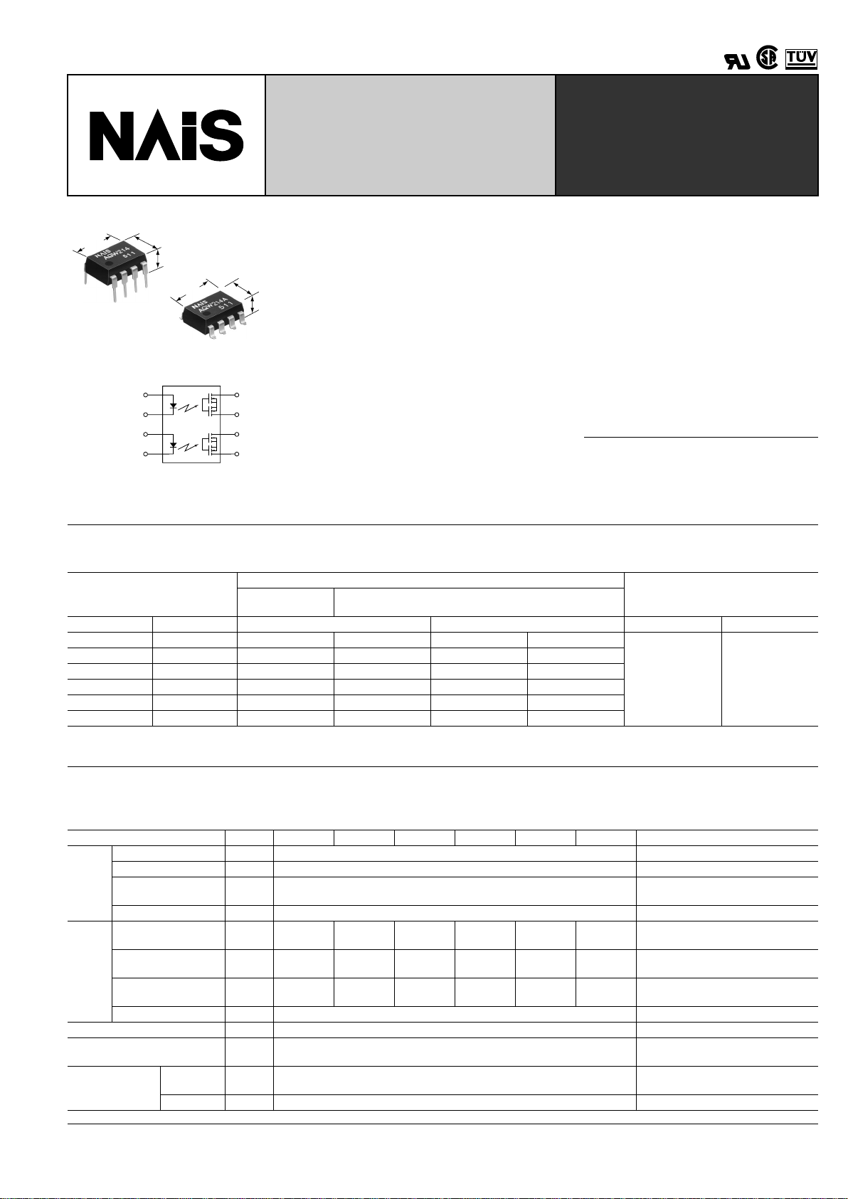
GU (General Use) Type
[2-Channel (Form A) Type]
mm inch
6.4
.252
9.78
.385
3.9±0.2
.154±.008
9.78
.385
6.4
.252
3.6±0.2
.142±.008
FEATURES
1. Compact 8-pin DIP size
The device comes in a compact (W) 6.4 ×
(L) 9.78 × (H) 3.9 mm (W) .252 × (L)
.385 × (H) .154 inch, 8-pin DIP size
(through hole terminal type).
2. Applicable for 2 Form A use as well
as two independent 1 Form A use
3. Controls low-level analog signals
PhotoMOS relays feature extremely low
closed-circuit offset voltage to enable
control of low-level analog signals without
distortion.
4. High sensitivity, high speed response
Can control a maximum 0.13 A load current with a 5 mA input current. Fast operation speed of 310 µ s (typical). (A QW214)
5. Low-level off state leakage current
The SSR has an off state leakage current
of several milliamperes whereas the PhotoMOS relays has only 100 pA even with
the rated load voltage of 400 V
(AQW214).
6. Low-level thermal electromotive
force (Approx. 1 µ V)
7. Eliminates the need for a counter
electromotive force pr otection diode in
the drive circuits on the input side
8. Stable ON resistance.
9. Eliminates the need for a po wer supply to drive the power MOSFET
TYPICAL APPLICATIONS
• High-speed inspection machines
• T elephones equipment
• Computer
TYPES
1. AC/DC type
*Indicate the peak AC and DC values.
Note: For space reasons, the package type indicator "X" and "Z" are omitted from the seal.
Output rating*
Part No.
Packing quantity
Through hole
terminal
Surface-mount terminal
Load voltage Load current Tube packing style Tape and reel packing style Tube Tape and reel
60V 350 mA AQW212 AQW212A AQW212AX AQW212AZ
1 tube contains
40 pcs.
1 batch contains
400 pcs.
1,000 pcs.
100 V 300 mA AQW215 AQW215A AQW215AX AQW215AZ
200 V 160 mA AQW217 AQW217A AQW217AX AQW217AZ
350 V 120 mA AQW210 AQW210A AQW210AX AQW210AZ
400 V 100 mA AQW214 AQW214A AQW214AX AQW214AZ
600 V 40 mA AQW216 AQW216A AQW216AX AQW216AZ
RATING
1. AC/DC type
1. Absolute maximum ratings (Ambient temperature: 25 ° C 77 ° F)
Item Symbol
AQW212(A) AQW215(A) AQW217(A) AQW210(A) AQW214(A) AQW216(A)
Remarks
Input
LED forward current I
F
50 mA
LED reverse voltage V
R
3 V
Peak forward current I
FP
1 A
f = 100 Hz,
Duty factor = 0.1%
Power dissipation P
in
75 mW
Output
Load voltage
(peak AC)
V
L
60 V 100 V 200 V 350 V 400 V 600 V
Continuous load
current
I
L
0.35 A
(0.40A)
0.30 A
(0.35 A)
0.16 A
(0.2 A)
0.12 A
(0.14 A)
0.10 A
(0.13 A)
0.04 A
(0.05 A)
( ): in case of using only 1 channel
A connection: Peak AC, DC
Peak load current I
peak
1.0 A 0.9 A 0.48 A 0.36 A 0.3 A 0.12 A
A connection: 100 ms (1 shot),
V
L
= DC
Power dissipation P
out
800 mW
Total power dissipation P
T
850 mW
I/O isolation voltage V
iso
1,500 V AC
Between input and output/
between contact sets
Temperature
limits
Operating T
opr
–40 ° C to +85 ° C –40 ° F to +185 ° F
Non-condensing at low
temperatures
Storage T
stg
–40 ° C to +100 ° C –40 ° F to +212 ° F
PhotoMOS
RELAYS
AQW21 ❍
58
2. Electrical characteristics (Ambient temperature: 25 ° C 77 ° F)
Note: Recommendable LED forward current I
F
= 5mA. For type of connection, see page 32.
*Turn on/Turn off time
■
For Dimensions, see Page 27.
■
For Schematic and Wiring Diagrams, see Page 32.
■
For Cautions for Use, see Page 36.
Item Symbol
AQW212(A) AQW215(A) AQW217(A) AQW210(A) AQW214(A) AQW216(A)
Condition
Input
LED operate
current
Typical
I
Fon
0.9 mA
I
L
= Max.
Maximum 3 mA
LED turn off
current
Minimum
I
Foff
0.4 mA
I
L
= Max.
Typical 0.8 mA
LED dropout
voltage
Typical
V
F
1.14 V (1.25 V at I
F
= 50 mA)
I
F
= 5 mA
Maximum 1.5 V
Output
On resistance
Typical
R
on
0.83 Ω
2.3 Ω
11 Ω
23 Ω
30 Ω
70 Ω I
F
= 5 mA
I
L
= Max.
Within 1 son time
Maximum 2.5 Ω
4.0 Ω
15 Ω
35 Ω
50 Ω
120 Ω
Off state leakage
current
Maximum I
Leak
1 µ A
I
F
= 0
V
L
= Max.
Transfer
characteristics
Turn on time*
Typical
T
on
0.65 ms 0.60 ms 0.25 ms 0.25 ms 0.31 ms 0.28 ms
I
F
= 5 mA
I
L
= Max.
Maximum 2 ms 2 ms 1.0 ms 0.5 ms 0.5 ms 0.5 ms
Turn off time*
Typical
T
off
0.08 ms 0.06 ms 0.05 ms 0.05 ms 0.05 ms 0.04 ms
I
F
= 5 mA
I
L
= Max.
Maximum 0.2 ms
I/O capacitance
Typical
C
iso
0.8 pF
f = 1 MHz
V
B
= 0
Maximum 1.5 pF
Initial I/C isolation
resistance
Minimum R
iso
1,000 M Ω
500 V DC
Ton
Input
Output 10%
90%
Toff
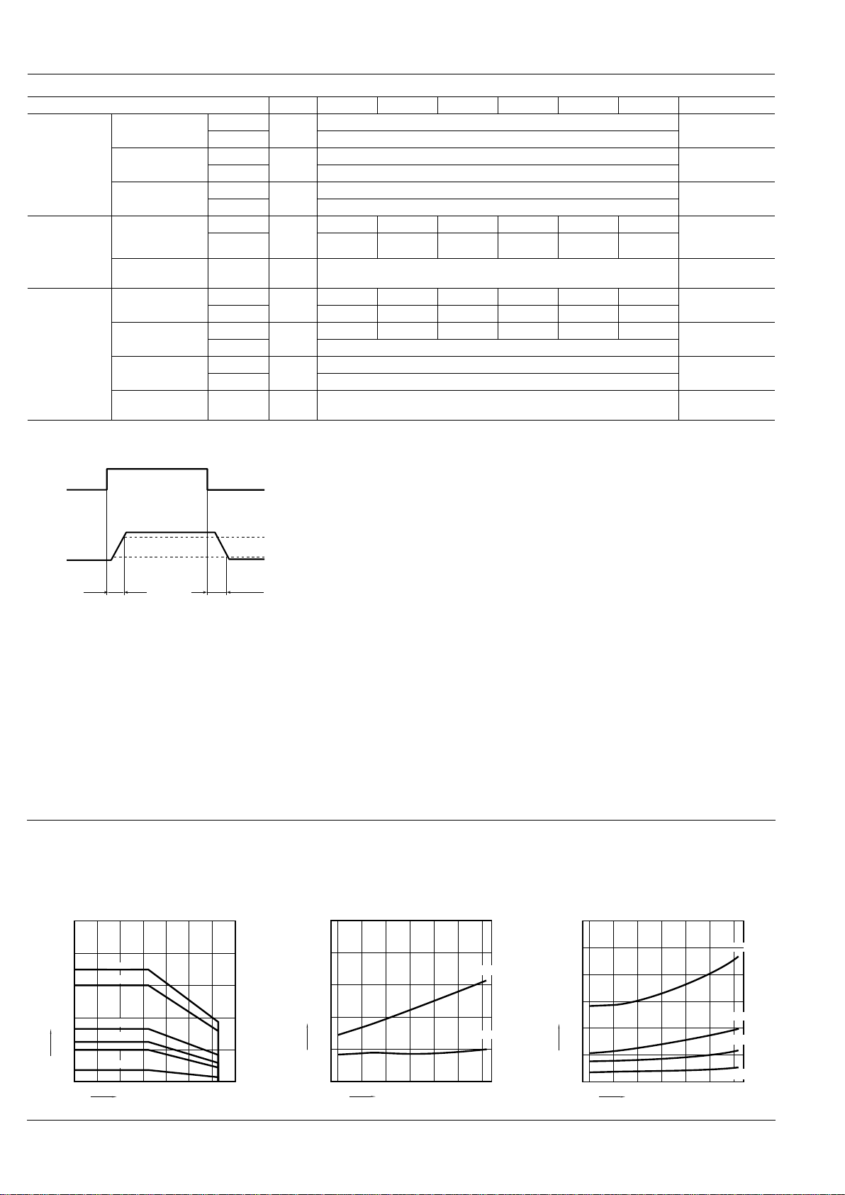
REFERENCE DATA
1. Load current vs. ambient temperature characteristics
Allowable ambient temperature: –40 ° C to +85 ° C
–40 ° F to +185 ° F
2.-(1) On resistance vs. ambient temperature
characteristics
Measured portion: between terminals 5 and 6, 7 and 8;
LED current: 5 mA; Load voltage: Max. (DC);
Continuous load current: Max. (DC)
2.-(2) On resistance vs. ambient temperature
characteristics
Measured portion: between terminals 5 and 6, 7 and 8;
LED current: 5 mA; Load voltage: Max. (DC);
Continuous load current: Max. (DC)
0
200
300
500
400
0204060
–20 8085100–40
100
AQW212
AQW215
AQW217
AQW210
AQW216
AQW214
Load current, mA
Ambient temperature, °C
0
1
2
3
4
–40
5
0–20 20 40 60 8085
AQW212
AQW215
On resistamce, Ω
Ambient temperature, °C
0
20
40
60
80
–40
120
0–20 20 40 60 8085
AQW216
100
AQW210
AQW217
AQW214
On resistamce, Ω
Ambient temperature, °C
 Loading...