

Page 1

SERVICE
SERVICE MANUAL
4
4
MMK-702U
DM802
Page 2

CONTENTS
1. PRECAUTIONS -----------------------------------------------------------------------------------------------------------------------2
1-1 SAFETY PRECAUTIONS------------------------------------------------------------------------------------------------------------2
1-2 SERVICING PRECAUTIONS--------------------------------------------------------------------------------------------------------3
1-2-1 General Serving Precautions------------------------------------------------------------------------------------------------3
1-2-2 Insulation Checking Procedure ---------------------------------------------------------------------------------------------4
1-3 ESD PRECAUTIONS ---------------------------------------------------------------------------------------------------------------4
2. REFERENCE INFORMATION ----------------------------------------------------------------------------------------------------5
2-1 COMPONENT DESCRIPTIONS-----------------------------------------------------------------------------------------------------5
2-1-1 DVD SONY HM-313PUH----------------------------------------------------------------------------------------------------5
2-1-2 DVD Processor Chip MTK1389D ------------------------------------------------------------------------------------------7
2-1-3 Serial EEPROM, 2K (256 x 8) (24C02) or 16 K (2048 x 8) (24C16)------------------------------------------------ 19
2-1-4: --------------------------------------------------- 20
Boot Sector Flash Memory 1M X 8 Bit / 512K X 16 Bit A29L800
2-1-5 2 Banks x 512K x 16 Bit Synchronous DRAM HY57V161610E ----------------------------------------------------- 24
3. PRODUCT SPECIFICATIONS --------------------------------------------------------------------------------------------------28
4. UPGRADING SYSTEM AND CHANGING THE REGION CODE------------------------------------------------------ 29
5. OPERATING INSTRUCTION---------------------------------------------------------------------------------------------------- 30
MAINTENANCE & TROUBLESHOOTING--------------------------------------------------------------------------------------------- 30
6.Problems and Solutions
7.TROUBLESHOOTING ------------------------------------------------------------------------------------------------------------- 32
8.RESOLVE DIAGRAM ------------------------------------------------------------------------------------------------------------- 33
9. BLOCK DIAGRAM ----------------------------------------------------------------------------------------------------------------- 34
10. CIRCUIT DIAGRAMS------------------------------------------------------------------------------------------------------------- 35
11. WIRING DIAGRAM:-------------------------------------------------------------------------------------------------------------- 49
----------------------------------------------------------------------------------------------------
31
- 1 -
Page 3
1. PRECAUTIONS
1-1 Safety Precautions
1) Before returning an instrument to the customer,
always make a safety check of the entire instrument,
including, but not limited to, the following items:
(1) Be sure that no built-in protective devices are
defective or have been defeated during servicing.
(1) Protective shields are provided to protect both
the technician and the customer. Correctly replace
all missing protective shields, including any
remove for servicing convenience.
(2) When reinstalling the chassis and/or other
assembly in the cabinet, be sure to put back in
place all protective devices, including, but not
limited to, nonmetallic control knobs, insulating
fish papers, adjustment and compartment
covers/shields, and isolation resistor/capacitor
networks. Do not operate this instrument or permit
it to be operated without all protective devices
correctly installed and functioning.
(2) Be sure that there are no cabinet opening through
which adults or children might be able to insert
their fingers and contact a hazardous voltage.
Such openings include, but are not limited to,
excessively wide cabinet ventilation slots, and an
improperly fitted and/or incorrectly secured
cabinet back cover.
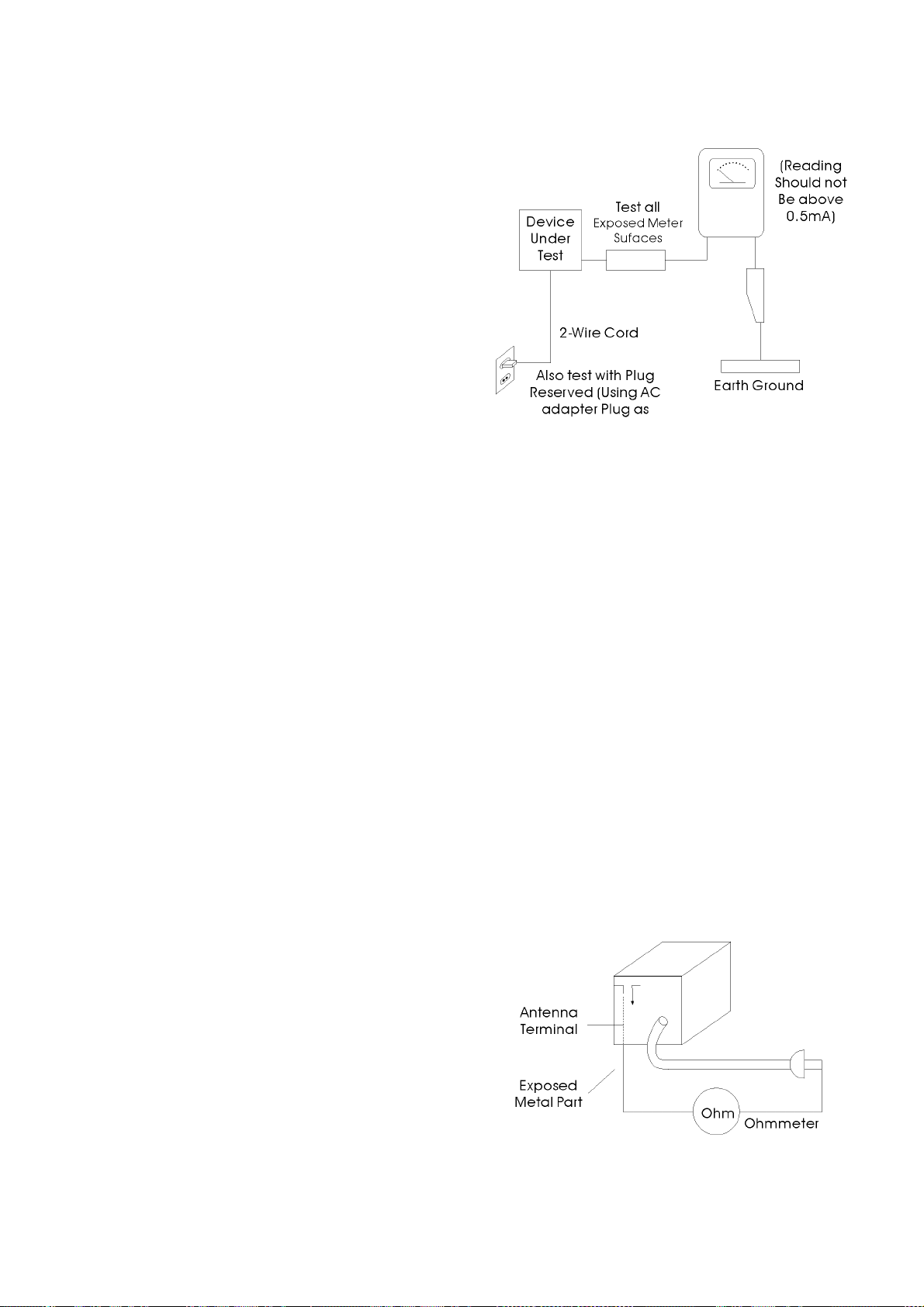
(3) Leakage Current Hot Check-With the instrument
completely reassembled, plug the AC line cord
directly into a 120V AC outlet. (Do not use an
isolation transformer during this test.) Use a
leakage current tester or a metering system that
complies with American National Standards
institute (ANSI) C101.1 Leakage.
Current for Appliances and underwriters
Laboratories (UL) 1270 (40.7). With the
instrument’s AC switch first in the ON position and
then in the OFF position, measure from a known
earth ground (metal water pipe, conduit, etc.) to all
exposed metal parts of the instrument (antennas,
handle brackets, metal cabinets, screwheads,
metallic overlays, control shafts, etc.), especially
and exposed metal parts that offer an electrical
return path to the chassis.
Any current measured must not exceed 0.5mA.
Reverse the instrument power cord plug in the
outlet and repeat the test.
AC Leakage Test
Any measurements not within the limits specified
herein indicate a potential shock hazard that must
be eliminated before returning the instrument to
the customer.
(4) Insulation Resistance Test Cold Check-(1) Unplug
the power supply cord and connect a jumper wore
between the two prongs of the plug. (2) Turn on
the power switch of the instrument. (3) Measure
the resistance with an ohmmeter between the
jumpered AC plug and all exposed metallic
cabinet parts on the instrument, such as
screwheads, antenna, control shafts, handle
brackets, etc. When an exposed metallic part has
a return path to the chassis, the reading should be
between 1 and 5.2 megohm. When there is no
return path to the chassis, the reading must be
infinite. If the reading is not within the limits
specified, there is the possibility of a shock hazard,
and the instrument must be re-pared and
rechecked before it is returned to the customer.
Insulation Resistance Test
- 2 -
Page 4

2) Read and comply with all caution and safety related
notes non or inside the cabinet, or on the chassis.
3) Design Alteration Warning-Do not alter of add to the
mechanical or electrical design of this instrument.
Design alterations and additions, including but not
limited to, circuit modifications and the addition of
items such as auxiliary audio output connections,
might alter the safety characteristics of this
instrument and create a hazard to the user. Any
design alterations or additions will make you, the
service, responsible for personal injury or property
damage resulting there from.
4) Observe original lead dress. Take extra care to
assure correct lead dress in the following areas:
(1) near sharp edges, (2) near thermally hot parts
(be sure that leads and components do not touch
thermally hot parts), (3) the AC supply, (4) high
voltage, and (5) antenna wiring. Always inspect in
all areas for pinched, out-of-place, or frayed wiring.
Do not change spacing between a component and
the printed-circuit board, Check the AC power
cord for damage.
5) Components, parts, and/or wiring that appear to
have overheated or that are otherwise damaged
should be replaced with components, parts and/or
wiring that meet original specifications.
Additionally determine the cause of overheating
and/or damage and, if necessary, take corrective
action to remove and potential safety hazard.
6) Product Safety Notice-Some electrical and
mechanical parts have special safety-related
characteristics which are often not evident from
visual inspection, nor can the protection they give
necessarily be obtained by replacing them with
components rated for higher voltage, wattage, etc.
Parts that have special safety characteristics are
identified by shading, an (
schematics and parts lists. Use of a substitute
replacement that does not have the same safety
characteristics as the recommended replacement
part might created shock, fire and/or other
hazards. Product safety is under review
continuously and new instructions are issued
whenever appropriate.
) or a ( ) on
1-2 Servicing Precautions
CAUTION: Before servicing Instruments covered by
this service manual and its supplements, read and
follow the Safety Precautions section of this manual.
Note: If unforeseen circument create conflict between
the following servicing precautions and any of the
safety precautions, always follow the safety
precautions. Remember; Safety First
1-2-1 General Serving Precautions
(1) a. Always unplug the instrument’s AC power cord
from the AC power source before (1) removing or
reinstalling any component, circuit board, module
or any other instrument assembly. (2)
disconnecting any instrument electrical plug or
other electrical connection. (3) connecting a test
substitute in parallel with an electrolytic capacitor
in the instrument.
b. Do not defeat any plug/socket B+ voltage
interlocks with which instruments covered by this
service manual might be equipped.
c. Do not apply AC power to this instrument and/or
any of its electrical assemblies unless all
solid-state device heat sinks are correctly
installed.
d. Always connect a test instrument’s ground lead
to the instrument chassis ground before
connecting the test instrument positive lead.
Always remove the test instrument ground lead
last.
Note: Refer to the Safety Precautions section
ground lead last.
(2) The service precautions are indicated or printed on
the cabinet, chassis or components. When
servicing, follow the printed or indicated service
precautions and service materials.
(3) The components used in the unit have a specified
flame resistance and dielectric strength.
When replacing components, use components
which have the same ratings, by (
in the circuit diagram are important for safety or
for the characteristics of the unit. Always replace
them with the exact replacement components.
(4) An insulation tube or tape is sometimes used and
some components are raised above the printed
wiring board for safety. The internal wiring is
sometimes clamped to prevent contact with
heating components. Install such elements as
they were.
(5) After servicing, always check that the removed
screws, components, and wiring have been
installed correctly and that the portion around the
serviced part has not been damaged and so on.
Further, check the insulation between the blades
of the attachment plus and accessible conductive
parts.
) or by ( )
- 3 -
Page 5

1-2-2 Insulation Checking Procedure
Disconnect the attachment plug from the AC outlet and
turn the power ON. Connect the insulation resistance
meter (500V) to the blades of the attachment plug. The
insulation resistance between each blade of the
1-3 ESD Precautions
attachment plug and accessible conductive parts (see
note) should be more than 1 Megohm.
Note: Accessible conductive parts include metal
panels, input terminals, earphone jacks, etc.
Electrostatically Sensitive Devices (ESD)
Some semiconductor (solid static electricity) devices
can be damaged easily by static electricity.
Such compo9nents commonly are called
Electrostatically Sensitive Devices (ESD). Examples of
typical ESD devices are integrated circuits and some
field-effect transistors and semiconductor chip
components. The following techniques of component
damage caused by static electricity.
(1) immediately before handling any semiconductor
components or semiconductor-equipped assembly,
drain off any electrostatic charge on your body by
touching a known earth ground. Alternatively,
obtain and wear a commercially available
discharging wrist strap device, which should be
removed for potential shock reasons prior to
applying power to the unit under test.
(2) after removing an electrical assembly equipped
with ESD devices, place the assembly on a
conductive surface such as aluminum foil, to
prevent electrostatic charge buildup or exposure
of the assembly.
(3) Use only a grounded-tip soldering iron to solder or
unsolder ESD device.
(4) Use only an anti-static solder removal devices.
Some solder removal devices not classified as
“anti-static” can generate electrical charges
sufficient to damage ESD devices.
(5) Do not use freon-propelled chemicals. These can
generate electrical charges sufficient to damage
ESD devices.
(6) Do not remove a replacement ESD device from its
protective package until immediately before you
are ready to install it. (Most replacement ES
devices are packaged with leads electrically
shorted together by conductive foam, aluminum
foil or comparable conductive materials).
(7) Immediately before removing the protective
materials from the leads of a replacement ES
device touch the protective material to the chassis
or circuit assembly into which the device will be
installed.
CAUTION: Be sure no power is applied to the chassis
or circuit, and observe all other safety precautions.
(8) Minimize bodily motions when handling
unpackaged replacement ESD devices.
(Otherwise harmless motion such as the brushing
together of your clothes fabric or the lifting of your
foot from a carpeted floor can generate static
electricity sufficient to damage an ESD device).
- 4 -
Page 6
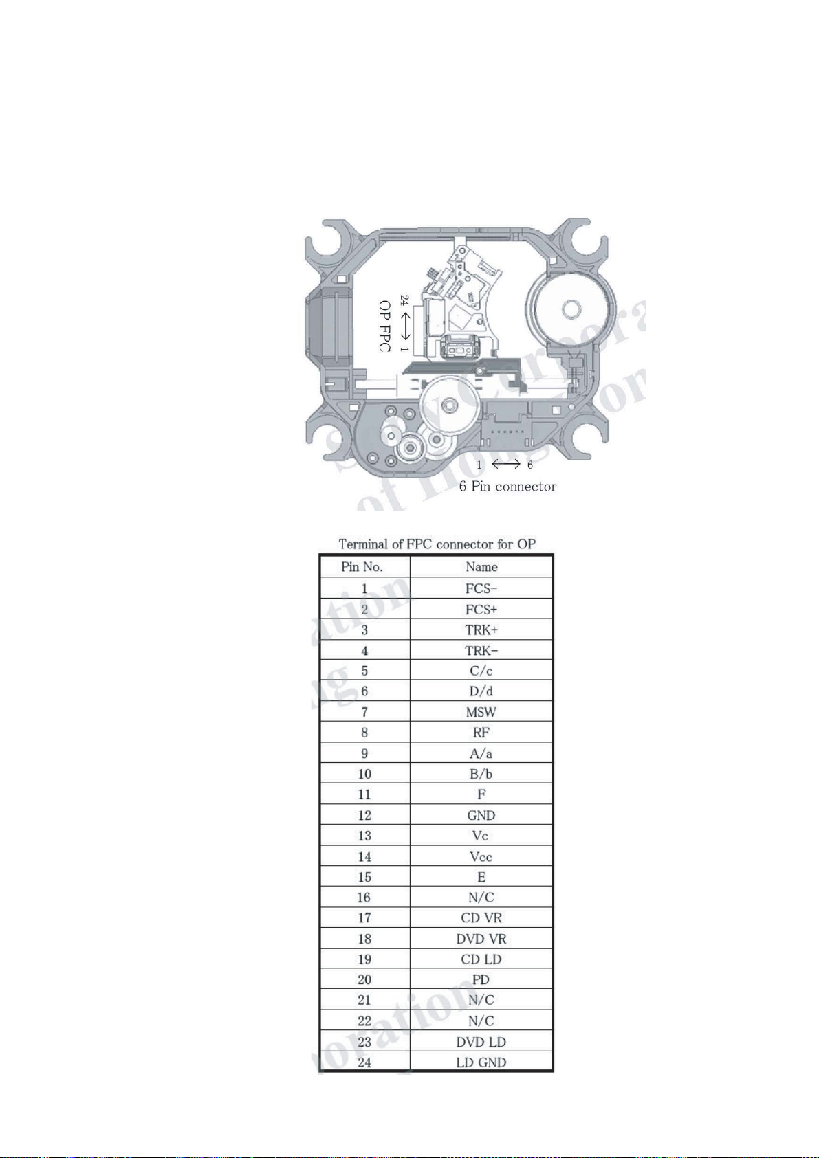
2. Reference Information
2-1 Component Descripti
2-1-1 DVD
Conn
SONY HM 313-
ector Pin Definition
PUH
ons
-5-
Page 7

V1.2
Desktop DVD Player SOC
PRELIMINARY, SUBJECT TO CHANGE WITHOUT NOTICE MTK CONFIDENTIAL, NO DISCLOSURE
MT1389L
1 Applications
This present specifications are applied to IC MT1389L.
2 Type
MT1389L
3 Usage
Single Chip IC for DVD Player
4 Structure
0.16um CMOS process, Silicon material, Monolithic IC, 128pin LQFP, 3.3/1.8 Dual operation voltages.
1
All information contained herein is the exclusive property of MediaTek Inc. and shall not be distributed, reproduced
or disclosed in whole or in part without prior written permission of MediaTek Inc
Page 8
V1.2
Desktop DVD Player SOC
PRELIMINARY, SUBJECT TO CHANGE WITHOUT NOTICE MTK CONFIDENTIAL, NO DISCLOSURE
MT1389L
5 Function
5-1 General Description
MediaTek MT1389L is a cost-effective DVD system-on-chip (SOC) which incorporates advanced features like
MPEG-4 video decoder, high quality TV encoder and state-of-art de-interlace processing. The MT1389L enables
consumer electronics manufacturers to build high quality, USB2.0, MS/SD/MMC reader, feature-rich DVD players,
portable DVD players or any other home entertainment audio/video devices.
World-Leading Technology: Based on MediaTek’s world-leading DVD player SOC architecture, the
MT1389L is the New generation of the DVD player SOC. It integrates the MediaTek 3
RF amplifier and the Servo/MPEG AV decoder.
Rich Feature for High Valued Product: To enrich the feature of DVD player, the MT1389 equips a
simplified MPEG-4 advanced simple profile (ASP) video decoder to fully support the DivX
makes the MT1389-based DVD player be capable of playback MPEG-4 content which become more and more
popular.
Incredible Audio/Video Quality: The progressive scan of the MT1389L utilized advanced motion-adaptive
de-interlace algorithm to achieve the best movie/video playback. It also supports a 3:2 pull down algorithm to give
the best film effect. The 108MHz/12-bit video DAC provides users a whole new viewing experience. Built-in 6ch
audio DACs and 2ch audio ADCs could give the variable function solutions.
High Performance Memory Storage Device: As the core of Portable DVD players need more capability to
support current multimedia contents. The MT1389L provides the interface for the 3-in-1 card reader, which
supports Memory-Stick, Secure Digital Memory Card, and MultiMediaCard, to connect with the mainstream digital
camera FLASH cards. For the USB application, we adopt USB2.0 High speed specification to reach rich-contents
transference. USB 2.0 High speed will support for high-speed devices. USB 2.0 High Speed is suitable for
high-performance devices such as high-density storage devices. In addition, USB 2.0 High Speed supports old
USB 1.0/1.1 software and peripherals, offering impressive and even better compatibility to customers
rd
generation front-end digital
1
Home Theater profile. It
Key Features
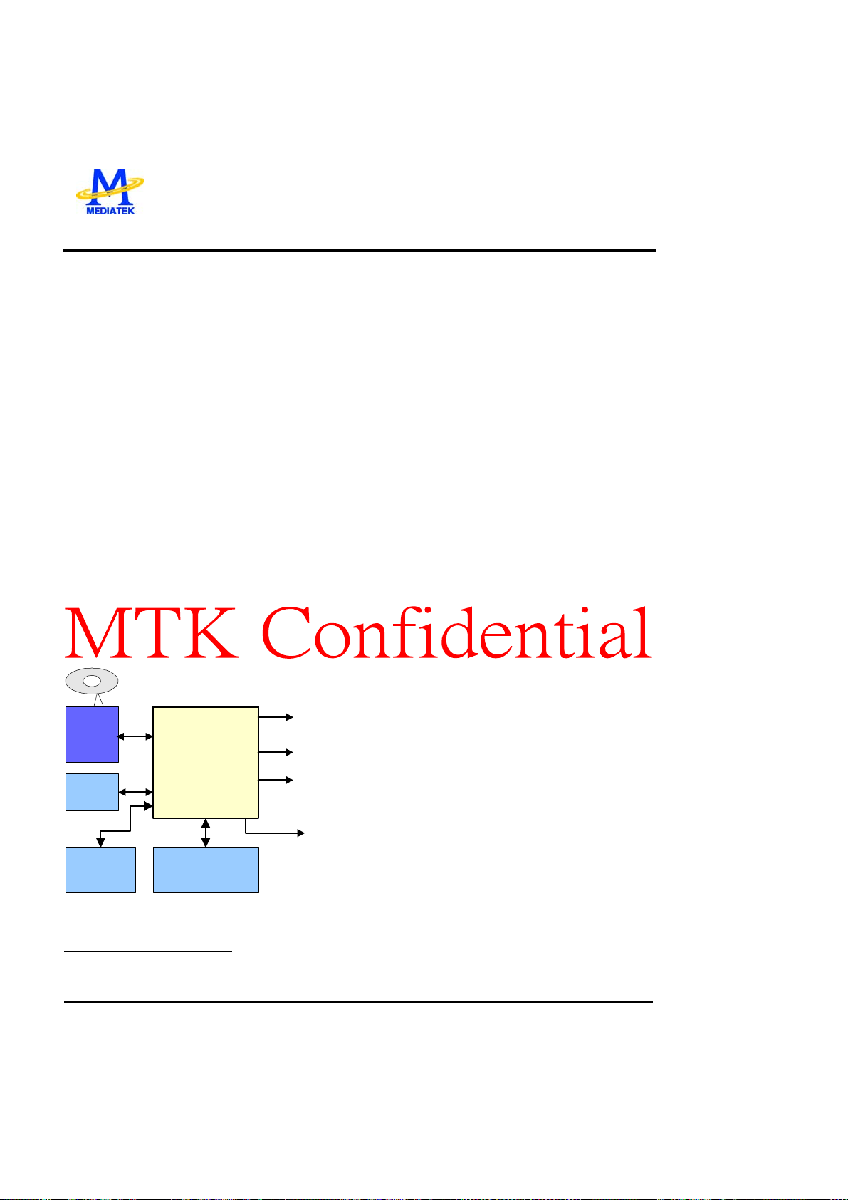
DVD
PUH
Module
FLASH
MT1389L
Desktop
CVBS, Y/C,
Component
SDPIF
Analog
Audio
Output
USB 2.0
High Speed
Front-panel
Remote
DRAM
DVD Player System Diagram Using MT1389L
1
DivX is a trademark of DivXNetworks
2
USB High Speed : 480Mbit/sec. USB Full Speed : 12Mbit/sec.
All information contained herein is the exclusive property of MediaTek Inc. and shall not be distributed, reproduced
or disclosed in whole or in part without prior written permission of MediaTek Inc
2
RF/Servo/MPEG Integration
DivX Home Theater Level MPEG4 ASP Video decoder
Support Nero-Digital
Support DivX Ultra
High Performance Audio Processor
Progressive Scan
108MHz/12-bit, 4 CH TV Encoder
Internal 6CH Audio DAC
Internal 2CH Audio ADC
USB2.0 High Speed (Host/Device)
3-in-1 MS/SD/MMC reader
Applications
Standard DVD Players
Page 9

V1.2
Desktop DVD Player SOC
PRELIMINARY, SUBJECT TO CHANGE WITHOUT NOTICE MTK CONFIDENTIAL, NO DISCLOSURE
5-2 Key Features
RF/Servo/MPEG Integration
Embedded 6ch Audio DAC
Embedded 2ch Audio ADC for Karaoke
High Performance Audio Processor
High Performance Progressive Video Processor
Support Nero-Digital
Support DivX Ultra
High Quality 108MHz/12-bit, 4 CH TV Encoder
USB 2.0 High-Speed
5-3 Applications
MT1389L
Standard DVD Players
DVD Players Home Theater Application
Portable DVD Players
TV/DVD Combo Systems
All information contained herein is the exclusive property of MediaTek Inc. and shall not be distributed, reproduced
or disclosed in whole or in part without prior written permission of MediaTek Inc
3
Page 10

V1.2
Desktop DVD Player SOC
PRELIMINARY, SUBJECT TO CHANGE WITHOUT NOTICE MTK CONFIDENTIAL, NO DISCLOSURE
5-4 General Feature lists
Super Integration DVD player single chip
High performance analog RF amplifier
Servo controller and data channel processing
MPEG-1/MPEG-2/JPEG video
Dolby AC-3/DTS Decoder
Unified memory architecture
Versatile video scaling & quality enhancement
OSD & Sub-picture
Built-in clock generator
Built-in high quality TV encoder
Built-in progressive video processor
Audio effect post-processor
Built-in 5.1-ch Audio DAC
Built-in 2-ch Audio ADC for Karaoke
USB 2.0 High-Speed
MS/SD/MMC 3-in-1 card reader
Speed Performance on Servo/Channel
Decoding
DVD-ROM up to 4XS
CD-ROM up to 24XS
Channel Data Processor
Digital data slicer for small jitter capability
Built-in high performance data PLL for channel
data demodulation
EFM/EFM+ data demodulation
Enhanced channel data frame sync protection
& DVD-ROM sector sync protection
Servo Control and Spindle Motor Control
Programmable frequency error gain and phase
error gain of spindle PLL to control spindle
motor on CLV and CAV mode
Built-in ADCs and DACs for digital servo
control
Provide 2 general PWM
Tray control can be PWM output or digital
output
Embedded Micro controller
Built-in 8032 micro controller
Built-in internal 373 and 8-bit programmable
lower address port
1024-bytes on-chip RAM
All information contained herein is the exclusive property of MediaTek Inc. and shall not be distributed, reproduced
or disclosed in whole or in part without prior written permission of MediaTek Inc
Up to 2M bytes FLASH-programming interface
Supports 5/3.3-Volt. FLASH interface
Supports power-down mode
Supports additional serial port
DVD-ROM/CD-ROM Decoding Logic
High-speed ECC logic capable of correcting
one error per each P-codeword or Q-codeword
Automatic sector Mode and Form detection
Automatic sector Header verification
Decoder Error Notification Interrupt that signals
various decoder errors
Provide error correction acceleration
Buffer Memory Controller
Supports 16Mb/32Mb/64Mb SDRAM
Supports 16-bit SDRAM data bus
Provides the self-refresh mode SDRAM
Block-based se ct or addressing
Video Decode
Decodes MPEG1 video and MPEG2 main level,
main profile video (720/480 and 720x576)
Decodes MPEG-4 Advanced Simple Profile
Support DivX 3.11/4.x/5.x Home Theater
Profile
Support Nero-Digital
Support DivX Ultra
Smooth digest view function with I, P and B
picture decoding
Baseline, extended-sequential and progressive
JPEG image decoding
Support CD-G titles
Video/OSD/SPU/HLI Processor
Arbitrary ratio vertical/horizontal scaling of
video, from 0.25X to 256X
65535/256/16/4/2-color bitmap format OSD,
256/16 color RLC format OSD
Automatic scrolling of OSD image
Audio Effect Processing
Dolby Digit al (AC- 3)/EX decoding
DTS/DTS-ES decoding
MPEG-1 layer 1/layer 2 audio decoding
4
MT1389L
Page 11

V1.2
MT1389L
Desktop DVD Player SOC
PRELIMINARY, SUBJECT TO CHANGE WITHOUT NOTICE MTK CONFIDENTIAL, NO DISCLOSURE
High Definition Compatible Digital (HDCD)
Windows Media Audio (WMA)
Dolby ProLogic II
Concurrent multi-channel and downmix out
IEC 60958/61937 output
- PCM / bit stream / mute mode
- Custom IEC latency up to 2 frames
Pink noise and white noise generator
Karaoke functions
- Microphone echo
- Microphone tone control
- Vocal mute/vocal assistant
- Key shift up to +/- 8 keys
- Chorus/Flanger/Harmony/Reverb
Channel equalizer
3D surround processing include virtual
surround and speaker separation
TV Encoder
Four 108MHz/12bit DACs
Support NTSC, PAL-BDGHINM, PAL-60
Support 525p, 625p progressive TV format
Automatically turn off unconnected channels
Support PC monitor (VGA)
Support Macrovision 7.1 L1, Macrovision 525P
and 625P
CGMS-A/WSS
Closed Caption
Progressive Scan Video
Automatic detect film or video source
3:2 pull down source detection
Advanced Motion adaptive de-interlace
Minimum external memory requirement
External Interface
USB2.0 High Speed (Host/Device)
Memory-Stick, Secure Digital Memory Card, and
MultiMediaCard Interface
Outline
128-pin LQFP package
3.3/1.8-Volt. Dual operating voltages
5
All information contained herein is the exclusive property of MediaTek Inc. and shall not be distributed, reproduced
or disclosed in whole or in part without prior written permission of MediaTek Inc
Page 12

V1.2
Desktop DVD Player SOC
PRELIMINARY, SUBJECT TO CHANGE WITHOUT NOTICE MTK CONFIDENTIAL, NO DISCLOSURE
MT1389L
Dolby License
Supply of this Implementation of Dolby technology does not convey a license nor imply a right
under any patent, or any other industrial or intellectual property right of Dolby Laboratories, to
use this Implementation in any finished end-user or ready-to-use final product. It is hereby
notified that a license for such use is required from Dolby Laboratories.
6
All information contained herein is the exclusive property of MediaTek Inc. and shall not be distributed, reproduced
or disclosed in whole or in part without prior written permission of MediaTek Inc
Page 13
V1.2
MT1389L
Desktop DVD Player SOC
PRELIMINARY, SUBJECT TO CHANGE WITHOUT NOTICE MTK CONFIDENTIAL, NO DISCLOSURE
5-5 Pin Definitions
Abbreviations:
y SR: Slew Rate
y PU: Pull Up
y PD: Pull Down
y SMT: Schmitt Trigger
y 4mA~16mA: Output buffer driving strength.
Pin Main Alt. Type Description
Analog Interface (66)
125
126
127
128
1
2
3
4
5
6
7
8
9 XTALI Input
10 XTALO Output
11
12
13
14
15
RFIP Analog Input AC coupled DVD RF signal input RFIP
RFIN OPOUT Analog Input AC coupled DVD RF signal input RFIN
RFG OPINP Analog Input Main beam, RF AC input path
RFH OPINN Analog Input Main beam, RF AC input path
RFA Analog Input RF main beam input A
RFB Analog Input RF main beam input B
RFC Analog Input RF main beam input C
RFD Analog Input RF main beam input D
RFE Analog Input RF sub beam input E
RFF Analog Input RF sub beam input E
AVDD18_2 Analog power Analog 1.8V power
AVDD33_1 Analog Power Analog 3.3V power
27MHz crys tal input
27MHz crystal output
AGND33 Analog Ground Analog Ground
V20
V14
REXT Analog Input
MDI1 Analog Input Laser power monitor input
Analog output Reference voltage 2.0V
Analog output Reference voltage 1.4V
Current reference input. It generates reference current for
RF path. Connect an external 15K resistor to this pin and
AVSS
7
All information contained herein is the exclusive property of MediaTek Inc. and shall not be distributed, reproduced
or disclosed in whole or in part without prior written permission of MediaTek Inc
Page 14
V1.2
MT1389L
Desktop DVD Player SOC
PRELIMINARY, SUBJECT TO CHANGE WITHOUT NOTICE MTK CONFIDENTIAL, NO DISCLOSURE
Pin Main Alt. Type Description
16 MDI2 Analog Input Laser power monitor input
17
18
19
20
21
22
23
24
25
26
27
28
29
30
31
32
95 DACVDDC Power
96 VREF Analog
97 FS Analog
98 DACVSSC Ground
99 CVBS
100 DACVDDB Power
101 DACVDDA Power
102 Y/G
103 B/CB/PB
LDO1 Analog Output Laser driver output
LDO2 Analog Output Laser driver output
AVDD33_2 Analog Power Analog 3.3V power
DMO Ana log Outp ut Disk motor control output. PWM output
FMO Analog Output Feed motor control. PWM output
TRAY_OPEN
TRAY_CLOSE
TRO
FOO
FG
USB_DP
USB_DM
VDD33_USB
VSS33_USB
PAD_VRT
VDD18_USB
Analog Output Tray PWM output/Tray open output
Analog Output
GPIO2
Analog Output
Analog Output
Analog
Analog Inout USB port DPLUS analog pin
Analog Inout USB port DMINUS analog pin
USB Power USB Power pin 3.3V
USB Ground USB ground pin
Analog Inout USB generating reference current
USB Power USB Power pin 1.8V
Analog
Analog
Analog
Tray PWM output/Tray close output
Tracking servo output. PDM output of tracking servo
compensator
Focus servo output. PDM output of focus servo
compensator
1) Motor Hall sensor input
2) GPIO
3.3V power pin for video DAC circuitry
Bandgap reference voltage
Full scale adjustment (suggest to use 560 ohm)
Ground pin for video DAC circuitry
Analog composite output
3.3V power pin for video DAC circuitry
3.3V power pin for video DAC circuitry
Green, Y, SY, or CVBS
Blue, CB/PB, or SC
All information contained herein is the exclusive property of MediaTek Inc. and shall not be distributed, reproduced
8
or disclosed in whole or in part without prior written permission of MediaTek Inc
Page 15
V1.2
MT1389L
Desktop DVD Player SOC
PRELIMINARY, SUBJECT TO CHANGE WITHOUT NOTICE MTK CONFIDENTIAL, NO DISCLOSURE
Pin Main Alt. Type Description
104 R/CR/PR
105 AADVSS Ground
106 AKIN2 Analog
107 ADVCM Analog
108 AKIN1 Analog
109 AADVDD Power
110 APLLVDD3 Power
111 APLLCAP Analog InOut
112 ADACVSS2 Ground
113 ADACVSS1 Ground
114 ARF / LFE GPIO Analog Output
115 ARS GPIO Analog Output
Analog Red, CR/PR, CVBS, or SY
Ground pin for 2ch audio ADC circuitry
1) Audio ADC input 2
2) MS_CLK set B
3) MCDATA
4) Audio Mute
5) HSYN/VSYN output
6) C5
7) GPIO
1) 2ch audio ADC reference voltageC
2) C6
3) GPIO
1) Audio ADC input 1
2) MS_D0 set B
3) Audio Mute
4) HSYN/VSYN output
5) C7
6) GPIO
3.3V power pin for 2ch audio ADC circuitry
3.3V Power pin for audio clock circuitry
APLL external capacitance connection
Ground pin for audio DAC circuitry
Ground pin for audio DAC circuitry
1) Audio DAC sub-woofer channel output
2) While internal audio DAC not used:
a. ACLK
b. GPIO
1) Audio DAC right Surround channel output
2) While internal audio DAC not used:
a. ABCK
b. GPIO
All information contained herein is the exclusive property of MediaTek Inc. and shall not be distributed, reproduced
9
or disclosed in whole or in part without prior written permission of MediaTek Inc
Page 16
V1.2
MT1389L
Desktop DVD Player SOC
PRELIMINARY, SUBJECT TO CHANGE WITHOUT NOTICE MTK CONFIDENTIAL, NO DISCLOSURE
Pin Main Alt. Type Description
1) Audio DAC right channel output
116 AR GPIO Analog Output
117 AVCM Analog
118 AL GPIO Analog Output
119 ALS GPIO Analog Output
ALF /CENTER
120
121 ADACVDD1 Analog Power
122 ADACVDD2 Analog Power
123 AVDD18_1 Analog Power
124 AGND18 Analog Ground
GPIO Analog Output
2) While internal audio DAC not used:
a. SDATA2
b. GPIO
c. RXD2
Audio DAC reference voltage
1) Audio DAC left channel output
2) While internal audio DAC not used:
a. SDATA1
b. GPIO
c. RXD1
1) Audio DAC left Surround channel output
2) While internal audio DAC not used:
a. ALRCK
b. GPIO
1) Audio DAC center channel output
2) While internal audio DAC not used:
a. ASDATA0
b. GPIO
3.3V power pin for audio DAC circuitry
3.3V power pin for audio DAC circuitry
Analog 1.8V power
Analog Ground
General Power/Ground (7)
54, 90 DVDD18 Power
79 DVSS18 Ground
50, 68,84 DVDD33 Power
60 DVSS Ground
Micro Controller , Flash Interface and GPIO(12)
InOut
33 GPIO3 INT#
34 GPIO4
8mA, SR
PD, SMT
InOut
4mA, PD
1.8V power pin for internal digital circuitry
1.8V Ground pin for internal digital circuitry
3.3V power pin for internal digital circuitry
3.3V Ground pin for internal digital circuitry
1) General purpose IO 3
2) Microcontroller external interrupt 1
General purpose IO 4
10
All information contained herein is the exclusive property of MediaTek Inc. and shall not be distributed, reproduced
or disclosed in whole or in part without prior written permission of MediaTek Inc
Page 17
V1.2
MT1389L
Desktop DVD Player SOC
PRELIMINARY, SUBJECT TO CHANGE WITHOUT NOTICE MTK CONFIDENTIAL, NO DISCLOSURE
Pin Main Alt. Type Description
35 GPIO6
36 SF_CS_
37 SF_DO
38 SF_DI
39 SF_CK
40 UP1_6 SCL
41 UP1_7 SDA
42 ICE
43 PRST#
44 IR
InOut
4mA, PD
InOut
8mA, SR
PU, SMT
InOut
8mA, SR
PD, SMT
InOut
8mA, SR
PU, SMT
InOut
8mA, SR
PD, SMT
InOut
4mA, SR
PU, SMT
InOut
4mA, SR
PU, SMT
Input
PD, SMT
Input
PU, SMT
Input
SMT
General purpose IO 6
Serial Flash Chip Select
Serial Flash Dout
Serial Flash Din
Serial Flash Clock
1) Microcontroller port 1-6
2
C clock pin
2) I
1) Microcontroller port 1-7
2
2) I
C data pin
Microcontroller ICE mode enable
Power on reset input, active low
IR control signal input
带格式的:
带格式的:
带格式的:
带格式的:
项目符号和编号
项目符号和编号
项目符号和编号
项目符号和编号
Dram Interface (37) (Sorted by position)
45 RD0
InOut,
4mA
DRAM data 0
11
All information contained herein is the exclusive property of MediaTek Inc. and shall not be distributed, reproduced
or disclosed in whole or in part without prior written permission of MediaTek Inc
Page 18
V1.2
MT1389L
Desktop DVD Player SOC
PRELIMINARY, SUBJECT TO CHANGE WITHOUT NOTICE MTK CONFIDENTIAL, NO DISCLOSURE
Pin Main Alt. Type Description
46 RD1
47 RD2
48 RD3
49 RD4
51 RD5
52 RD6
53 RD7
55 DQM0
56 RD15
57 RD14
58 RD13
59 RD12
61 RD11
62 RD10
63 RD9
64 RD8
InOut
4mA
InOut
4mA
InOut
4mA
InOut
4mA
InOut
4mA
InOut
4mA
InOut
4mA
InOut
4mA, PD
InOut
4mA
InOut
4mA
InOut
4mA
InOut
4mA
InOut
4mA
InOut
4mA
InOut
4mA
InOut
4mA
DRAM data 1
DRAM data 2
DRAM data 3
DRAM data 4
DRAM data 5
DRAM data 6
DRAM data 7
Data mask 0
DRAM data 15
DRAM data 14
DRAM data 13
DRAM data 12
DRAM data 11
DRAM data 10
DRAM data 9
DRAM data 8
12
All information contained herein is the exclusive property of MediaTek Inc. and shall not be distributed, reproduced
or disclosed in whole or in part without prior written permission of MediaTek Inc
Page 19

V1.2
MT1389L
Desktop DVD Player SOC
PRELIMINARY, SUBJECT TO CHANGE WITHOUT NOTICE MTK CONFIDENTIAL, NO DISCLOSURE
Pin Main Alt. Type Description
65 DQM1
66 RCLK
67 RA11
69 RA9
70 RA8
71 RA7
72 RA6
73 RA5
74 RA4
75 RWE#
76 CAS#
77 RAS#
78 BA0
80 BA1
81 RA10
InOut
4mA, PD
InOut
4mA, PD
InOut
4mA, PD
InOut
4mA, PD
InOut
4mA, PD
InOut
4mA, PD
InOut
4mA, PD
InOut
4mA, PD
InOut
4mA, PD
Output
4mA, PD
Output
4mA, PD
Output
4mA, PD
InOut
4mA, PD
InOut
4mA, PD
InOut
4mA, PD
Data mask 1
Dram clock
DRAM address bit 11
DRAM address 9
DRAM address 8
DRAM address 7
DRAM address 6
DRAM address 5
DRAM address 4
DRAM Write enable, active low
DRAM column address strobe, active low
DRAM row address strobe, active low
DRAM bank address 0
DRAM bank address 1
DRAM address 10
All information contained herein is the exclusive property of MediaTek Inc. and shall not be distributed, reproduced
13
or disclosed in whole or in part without prior written permission of MediaTek Inc
Page 20

V1.2
MT1389L
Desktop DVD Player SOC
PRELIMINARY, SUBJECT TO CHANGE WITHOUT NOTICE MTK CONFIDENTIAL, NO DISCLOSURE
Pin Main Alt. Type Description
82 RA0
83 RA1
85 RA2
86 RA3
87 GPIO7 CKE
InOut
4mA, PD
InOut
4mA, PD
InOut
4mA, PD
InOut
4mA, PD
InOut
4mA, PD
DRAM address 0
DRAM address 1
DRAM address 2
DRAM address 3
1) GPIO 7
2) Dram Clock Enable
3) MS_CLK set A
4) Audio Mute
5) HSYN/VSYN input
6) C0
GPIO (6)
1) GPIO8
2) MS_BS set A
3) SD_CLK set A
88 GPIO8
89 GPIO9
InOut
4mA, PD
InOut
4mA, PU
4) ASDATA2
5) ACLK
6) Audio Mute
7) HSYN/VSYN input
8) C1
1) GPIO9
2) MS_D0 set A
3) SD_CMD set A
4) ASDATA1
5) ABCK
6) C2
7) RXD1
14
All information contained herein is the exclusive property of MediaTek Inc. and shall not be distributed, reproduced
or disclosed in whole or in part without prior written permission of MediaTek Inc
Page 21

V1.2
MT1389L
Desktop DVD Player SOC
PRELIMINARY, SUBJECT TO CHANGE WITHOUT NOTICE MTK CONFIDENTIAL, NO DISCLOSURE
Pin Main Alt. Type Description
1) GPIO10
2) SD_CLK set B
3) SD_D0 set A
91 GPIO10
92 GPIO11
93 SPDIF GPIO12
94 GPIO13
InOut
4mA, PD
InOut
4mA, PD
InOut
2mA, PD
InOut
4mA, PD
4) ASDATA0
5) ALRCK
6) HSYN/VSYN output
7) C3
8) TXD1
1) GPIO11
2) SD_CMD set B
3) MS_BS set B
4) Audio Mute
5) HSYN/VSYN output
6) C4
1) SPDIF output
2) GPIO12
1) GPIO13
2) SD_D0 set B
3) ALRCK
4) Audio Mute
5) YUVCLK
Note:
1. The Main column is the main function, Alt. means alternative function.
2. The multi-function GPIO pins are set to green characters.
15
All information contained herein is the exclusive property of MediaTek Inc. and shall not be distributed, reproduced
or disclosed in whole or in part without prior written permission of MediaTek Inc
Page 22

V1.2
MT1389L
Desktop DVD Player SOC
PRELIMINARY, SUBJECT TO CHANGE WITHOUT NOTICE MTK CONFIDENTIAL, NO DISCLOSURE
5-6 Functional Block
DVD
PUH
Module
Motor
Drive
FLASH
ROM
DRAM
GPIO
IR/VFD
RF Amplifier
Servo IO
Spindle
Control
Memory
Controller
System
CPU
Debug
Servo
Processor
Audio
DSP
System
Parser
CPPM/CPRM
DRM
32-bit
RISC
Port
108MHz
TV Encoder
Video
Processor
Audio
Ouptut
Video DAC
interlacer
MPEG-1/2/4
JPEG
Video Decoder
6ch Audio DACs
De-
Internal
PCM output
Internal
Audio ADC
CVBS, Y/C
Component
Video
6ch Audio Analog
outputs
Audio
DAC
SDPIF
Audio Mic1
Audio Mic2
USB 2.0 High
Speed
controller
MS/SD/MMC
Card
Controller
USB 2.0 High
/ Full Speed
Device
MS/SD/MMC
Flash Card
16
All information contained herein is the exclusive property of MediaTek Inc. and shall not be distributed, reproduced
or disclosed in whole or in part without prior written permission of MediaTek Inc
Page 23

V1.2
GPIO13
AudioAudioVid
DAC
ADC
DAC
_
DVDD18
INT RF
GPIO9
XTALI
GPIO8
XTALO
GPIO7 / CKE
V20
V14
REXT
USB
DVSS18
_
_
MT1389L
Desktop DVD Player SOC
PRELIMINARY, SUBJECT TO CHANGE WITHOUT NOTICE MTK CONFIDENTIAL, NO DISCLOSURE
6 Pin Assignment
AKIN1 / GPIO21 / Audio_mute
AKIN2 / GPIO19 / Audio_mute
ALF / CENTER / GPIO
RFH / OPINN /
RFIN / OPOUT /
RFG / OPINP /
128
127
126
1 96 VREF
RFA
2 95 DACVDDC
RFB
3 94
RFC
4
RFD
5
RFE
6 91 GPIO10
RFF
7 90
2
AVDD18
AVDD33_1
AGND33
AVDD33_2
TRAY
TRAY
FG / GPIO2 26 71 RA7
USB_DP 27 70 RA8
USB_DM 28 69 RA9
VDD33_USB 29 68 DVDD33
VSS33_USB 30 67 RA11
PAD_VRT 31 66 RCLK
VDD18_USB 32 65 DQM1
8
9 88
10 87
11 86 RA3
12 85 RA2
13 84 DVDD33
14 83 RA1
15 82 RA0
MDI1
16 81 RA10
MDI2
17 80 BA1
LDO1
18
LDO2
19 78 BA0
20 77 RAS#
DMO
21 76 CAS#
FMO
22 75 RWE#
OPEN
23 74 RA4
CLOSE
24 73 RA5
TRO
25 72 RA6
FOO
33343536373839404142434445464748495051525354555657585960616263
GPIO3 / INT#
GPIO4
GPIO6
RFIP
125
SF_CS_
AGND18
124
SF_DO
AVDD18_1
123
SF_DI
ADACVDD2
122
SF_CK
ADACVDD1
121
UP1_6 / SCL
120
UP1_7 / SDA
ALS / GPIO
119
ICE
AL / GPIO1
118
PRST#IRRD0
ARF / LFE / GPIO
ARS / GPIO
ADACVSS1
115
114
ADACVSS2
113
112
APLLCAP
111
AR / GPIO0
AVCM
117
116
MT1389L
Desktop
RD1
RD2
RD3
RD4
DVDD33
APLLVDD
110
RD5
AADVDD
109
RD6
108
RD7
ADVCM / GPIO20 /
107
DVDD18
106
DQM0
AADVSS
R
105
104
RD15
RD14
B
103
RD13
G
102
RD12
eo
DACVDDA
101
DVSS33
DACVDDB
100
RD11
DACVSSC
CVBS
FS
999897
93 SPDIF / GPIO12
92 GPIO11
89
79
64
RD10
RD9
RD8
17
All information contained herein is the exclusive property of MediaTek Inc. and shall not be distributed, reproduced
or disclosed in whole or in part without prior written permission of MediaTek Inc
Page 24

V1.2
MT1389L
Desktop DVD Player SOC
PRELIMINARY, SUBJECT TO CHANGE WITHOUT NOTICE MTK CONFIDENTIAL, NO DISCLOSURE
7 Absolute Maximum Ratin gs
Symbol Parameters Value Unit
VDD3 3.3V Supply voltage -0.3 to 3.6 V
VDD2 1.8V Supply voltage -0.3 to 2.1 V
VDDA Analog Supply voltage -0.3 to 3.6 V
VIN(3.3V) Input Voltage (3.3V IO) -0.3 to 3.63 V
VIN(5V-tolerance) Input Voltage (5V-tolerance IO) -0.3 to 5.5 V
V
Output Voltage -0.3 to VDD3+0.3 V
OUT
T
Storage Temperature -45 to 150
STG
o
C
8 Recommend Operation Condition
Symbol Parameters Min Typ Max Unit
TOP Operating Temperature 0 70 oC
TJ Junction Operation Temp. 0 25 115 oC
VDD3 3.3V Supply voltage 3.0 3.3 3.6 V
VDD2 1.8V Supply voltage 1.7 1.8 2.0 V
VDDA Analog Supply voltage 3.0 3.3 3.6 V
VIH (1.8V) Input voltage high (1.8V IO) 1.05 - - V
VIL (1.8V) Input voltage low (1.8V IO) - - 0.69 V
VIH (3.3V) Input voltage high (3.3V IO) 2.0 - - V
VIL (3.3V) Input voltage low (3.3V IO) - - 0.8 V
IIH High level input current 10 UA
IIL Low level input current -10 UA
PD Power dissipation 1.5 W
P
Power down mode 0.1 W
DOWN
fclk Input frequency of clock 27 MHz
18
All information contained herein is the exclusive property of MediaTek Inc. and shall not be distributed, reproduced
or disclosed in whole or in part without prior written permission of MediaTek Inc
Page 25

V1.2
MT1389L
Desktop DVD Player SOC
PRELIMINARY, SUBJECT TO CHANGE WITHOUT NOTICE MTK CONFIDENTIAL, NO DISCLOSURE
9 Electrical Characteristi cs
9-1 DC Characteristics
Symbol Parameters Min Typ Max Unit
VOH (1.8V)
VOL (1.8V)
VOH (3.3V)
VOL (3.3V)
Output voltage high (1.8V IO)
Output voltage low (1.8V IO)
Output voltage high (3.3V IO)
Output voltage low (3.3V IO)
(*IOH = 2 ~ 16mA)
(*IOL = 2 ~ 16mA)
(*IOH = 2 ~ 16mA)
(*IOL = 2 ~ 16mA)
Rpu Pull-up Resistance 40 75 190
Rpd Pull-down Resistance 40 75 190
FOO
Offset voltage between FOO zero output and V
OFF
TRO
Offset voltage between TRO zero output and V
OFF
DMO
Offset voltage between DMO zero output and V
OFF
-50 0 50 mV
REF
-40 0 40 mV
REF
-30 0 30 mV
REF
Note * : The driving current of some IO pad are programmable according to the different application and
environment . All setting will be defined according to the F/W progress and test result.
Built-in Audio- DAC Characteristics
9-2
Note *: All parameters is measured on MediaTek’s DVD player reference DVD board, the actual performance depends on
different PCB desig n.
SYMBOL PARAMETER MIN. TYP. MAX. UNIT
Output swing level:
V
out
Digital i/p level =0 dBFS , ADACVDD =3.3V
= 1.0 * ADACVDD / 3.3)
(V
out
Ro Output impedance @ 1kHz 50 100
RL_
Minimum resister load 5 K
min
CL_
Maximum capacitor load 20 PF
max
S/(THD+N)
S/(THD+N) @ 0 dBFS;
= 1kHz; Fs = 48kHz, A-weighted
f
in
DR Dynamic Range 88 dBr(A)
SNR Signal to noise ratio; A-weighted 95 dBr(A)
Channel
Separation
Close-talk of Left and Right Channel 85 dB
9-3 Built-in Video-DAC Specifications
Input Codes for Video Application:
NTSC NTSC w/setup 525_I 525_I w/setup 525_P
WHITE (235) Programable, Programable, Programable, Programable, Programable,
19
All information contained herein is the exclusive property of MediaTek Inc. and shall not be distributed, reproduced
or disclosed in whole or in part without prior written permission of MediaTek Inc
1.22 - - V
- - 0.4 V
2.4 - - V
- - 0.4 V
KΩ
KΩ
0.9 1.0 1.1 V
P
90 dBr(A)
带格式的:
带格式的:
项目符号和编号
项目符号和编号
Page 26

V1.2
MT1389L
Desktop DVD Player SOC
PRELIMINARY, SUBJECT TO CHANGE WITHOUT NOTICE MTK CONFIDENTIAL, NO DISCLOSURE
Current setting:
3297
Current setting:
3297
Current setting:
3297
Current setting:
3297
Current setting:
3290
BLACK (16) 960 1120 960 1120 1008
PEDESTAL 960 960 960 960 1008
SYNC TIP 64 64 64 64 64
525_P w/s PAL 625_I 625_P RGB
WHITE (235) ---
Programable,
Current setting:
3290
Programable,
Current setting:
3290
Programable,
Current setting:
3290
Programable,
Current setting:
2282
BLACK (16) --- 1008 1008 1008 0
PEDESTAL --- 1008 1008 1008 -
SYNC TIP --- 64 64 64 -
9-4 Video Output Voltage Level:
High Impedance Mode:
I
(max) = 19.4152 / R
OUT
(max) = R
V
OUT
= D
V
OUT
/ 4095 * V
IN
LOAD
, R
REF
* I
(max) = 1.3237 V, R
OUT
(max) = D
OUT
= 2.2 KOhm
REF
* R
IN
LOAD
= 150 Ohm
LOAD
* 0.0047412 / R
REF
Low Impedance Mode:
I
(max) = 19.4152 / R
OUT
(max) = R
V
OUT
= D
V
OUT
/ 4095 * V
IN
LOAD
, R
REF
* I
(max) = 1.3 V, R
OUT
(max) = D
OUT
= 560 Ohm
REF
* R
IN
= 37.5 Ohm ( 75 Ohm || 75 Ohm )
LOAD
* 0.0047412 / R
LOAD
REF
9-5 Video DAC DC Electrical Characteristics
(Operating Free-Air Temperature, AVDD 3.3V, DVDD = 3.3V).
Analog Output MIN TYP MAX UNIT
Full Scale Output Current CVBS/Y/C/R/G/B (low impedance mode) 33.6 34.6 34.9 mA
Full Scale Output Current CVBS/Y/C/R/G/B (high impedance mode) 8.40 8.65 8.73 mA
LSB current CVBS/Y/C/R/G/B (low impedance mode) 32.8 33.8 34.1 uA
LSB current CVBS/Y/C/R/G/B (high impedance mode) 8.20 8.45 8.52 uA
DAC-to-DAC Mis-Matching -- 1.28 -- %
Output Compliance 0 -- 1.35 V
带格式的:
项目符号和编号
All information contained herein is the exclusive property of MediaTek Inc. and shall not be distributed, reproduced
20
or disclosed in whole or in part without prior written permission of MediaTek Inc
Page 27

V1.2
MT1389L
Desktop DVD Player SOC
PRELIMINARY, SUBJECT TO CHANGE WITHOUT NOTICE MTK CONFIDENTIAL, NO DISCLOSURE
DAC Output Delay -- 1.5 10 ns
DAC Rise/Fall Time -- 2.1 5
Voltage Reference
Reference Voltage Output 1.27 V
Reference Input Current 2.267 MA
Static Performance
DAC Resolution 12 Bits
DNL Differential Non-Linearity +/-0.2 */-0.25 +/-0.3 LSB
INL Integral Non-Linearity +/-0.35 */-0.4 +/-0.49 LSB
Dynamic Performance
Differential Gain 0.8 1.5 %
Differential Phase 0.6 1.5 ∘
S/N Ratio 70 dB
Power Supply
Supply Voltage 3.0 3.3 3.6 V
RF specification
9-6
带格式的:
项目符号和编号
Item Designator Conditions Min Typ Max Unit
3.3V POWER 3.00 3.30 3.60 Volts
Power Down Mode
Reference Voltage V20 Force current =0A 1.85 1.99 2.15 Volts
Reference Voltage VREFO Force current =0A 1.25 1.39 1.55 Volts
Reference Voltage V2REFO Force current =0A 2.65 2.78 2.95 Volts
MDI1
APC1(CD)
APC2(DVD)
LDO1 0Ah=00 ;APC1 off 3.00 3.28 V
MDI1→LDO1
MDI2
Enable power down 10 27 50 mA
Chip Reset 90 151 200 mA
0Ah=10 ;APC1 on
MDI1=180mV
0Ah=10; APC1 on 212 254 295 V/V
0Bh=10 ;APC2 on
MDI2=180mV
166 184 202 mV
166 184 202 mV
21
All information contained herein is the exclusive property of MediaTek Inc. and shall not be distributed, reproduced
or disclosed in whole or in part without prior written permission of MediaTek Inc
Page 28

V1.2
MT1389L
Desktop DVD Player SOC
PRELIMINARY, SUBJECT TO CHANGE WITHOUT NOTICE MTK CONFIDENTIAL, NO DISCLOSURE
Item Designator Conditions Min Typ Max Unit
LDO2 0Bh=00 ;APC2 off 3.00 3.28 V
Focusing Error Ga in
Focusing Error Frequency
Response
Focusing Error Commo n
Mode Gain
Focusing Error H/L Gain
Focusing Error off set
Adjustment step
Focusing Error THD
Central Servo Gain
Central Servo Frequency
Response
Central Servo Common
Mode Gain
MDI2→LDO2
MA → FEO
MA → FEO
MA → FEO
MB → FEO
MA → FEO
Input Floating
Measure FEO
MA → FEO
MA → CSO
MA → CSO
MA → CSO
MB → CSO
0Bh=10; APC2 on
High gain
05h=30; low gain
With 10KHz Sin Input
05h=7C; low gain
With 10KHz, 300KHz Sin Input
R=G(10kHz)-G(300Khz)
05h=3F; low gain
With 10KHz Sin Input
Toggle 05h bit5 : FELG
With 10KHz Sin Input
Toggle 4Dh : FEOS[6:0] 65 103 140 mV
05h=7C; low gain
With 10KHz Sin Input
06h=F0; low gain
With 10KHz Sin Input
06h=FF; low gain
With 10KHz, 300KHz Sin Input
R=G(10kHz)-G(300Khz)
06h=F0; low gain
With 10KHz Sin Input
210 265 298 V/V
7.5 10.3 11.5 dB
16 23.9 dB
-34 -20 dB
2.75 2.99 3.25 V/V
30 54 dB
12.5 14.1 15.5 dB
14 21.4 dB
-30 -10 dB
Central Servo H/L Gain
Central Servo offset
Adjustment step
MA → CSO
Input Floating
Measure CSO
Toggle 06h bit5 : CSOLG
With 10KHz Sin Input
Toggle 4Eh : CSOOS[6:0] 65 108 140 mV
2.75 2.97 3.25 V/V
22
All information contained herein is the exclusive property of MediaTek Inc. and shall not be distributed, reproduced
or disclosed in whole or in part without prior written permission of MediaTek Inc
Page 29

V1.2
MT1389L
Desktop DVD Player SOC
PRELIMINARY, SUBJECT TO CHANGE WITHOUT NOTICE MTK CONFIDENTIAL, NO DISCLOSURE
Item Designator Conditions Min Typ Max Unit
Central Servo THD
Tracking Error Gain
Tracking Error Frequency
Response
Tracking Error Common
Mode Gain
Tracking Error H/L Gain
Tracking Error offset
Adjustment step
Tracking Error THD
RFL Gain
RFL Frequency Response
RFL H/L Gain I
RFL H/L Gain II
RFL offset Adjustment
step
RFL THD
MA → CSO
MA → TEO
MA → TEO
MA → TEO
MB → TEO
MA → TEO
Input Floating
Measure TEO
MA → TEO
MA → LVL
MA → LVL
MA → LVL
SA → LVL
Input Floating
Measure LVL
MA → LVL
06h=F0; low gain
With 10KHz Sin Input
07h=70; low gain
With 10KHz Sin Input
07h=70; low gain
With 10KHz, 300KHz Sin Input
R=G(10kHz)-G(300Khz)
07h=7F; low gain
With 10KHz Sin Input
Toggle 07h bit6, 5
With 10KHz Sin Input
Toggle 4Fh : TEOS[6:0] 65 110 140 mV
07h=7F; low gain
With 10KHz Sin Input
08h=60; low gain
With 10KHz Sin Input
08h=7F; low gain
With 10KHz, 300KHz Sin Input
R=G(10kHz)-G(300Khz)
Toggle 09h bit1 : LVLATN
With 10KHz Sin Input
Toggle 09h bit2 : SBADHG
With 10KHz Sin Input
Toggle 50h : LVLOS[6:0] 65 113 140 mV
08h=7F; low gain
With 10KHz Sin Input
30 53 dB
13 15 17 dB
16 24.2 dB
-22 -10 dB
4 5.8 8 V/V
30 42 dB
-6.5 -4.6 -3.5 dB
14 22.7 dB
0.3 0.52 0.7 V/V
2.5 2.77 3.1 V/V
30 44 dB
23
All information contained herein is the exclusive property of MediaTek Inc. and shall not be distributed, reproduced
or disclosed in whole or in part without prior written permission of MediaTek Inc
Page 30

V1.2
MT1389L
Desktop DVD Player SOC
PRELIMINARY, SUBJECT TO CHANGE WITHOUT NOTICE MTK CONFIDENTIAL, NO DISCLOSURE
Micro Controller Interface
9-7
Parameter Symbol Min. Max. Units
Oscillator Frequency 1/Tf 0 23.3 MHz
ALE Pulse Width T0 1.5Tf-5 ns
ALE Low to Valid Instruction T1 2.5Tf-20 ns
ALE Low to PSEN Low T5 0.5Tf-5 ns
Address Valid to ALE Low T2 0.5Tf-5 ns
Address Hold After ALE Low T9 0.5Tf-5 ns
PSEN Pulse Width T3 2.0Tf-5 ns
PSEN Low to Valid Instruction T4 2.0Tf-20 ns
Input Instruction Hold Aft e r PSE N high T8 0 ns
Input Instruction Float After PSEN high T6 1.0Tf-5 ns
Port 0 Address to Valid Instruction T10 3.0Tf-20 ns
Port 2 Address to Valid Instruction T11 3.5Tf-20 ns
PSEN Low to Address Float T7 0 ns
带格式的:
项目符号和编号
All information contained herein is the exclusive property of MediaTek Inc. and shall not be distributed, reproduced
24
or disclosed in whole or in part without prior written permission of MediaTek Inc
Page 31

V1.2
Desktop DVD Player SOC
PRELIMINARY, SUBJECT TO CHANGE WITHOUT NOTICE MTK CONFIDENTIAL, NO DISCLOSURE
t0 t1
MT1389L
ALE
PSEN
Port 0
Port 2
Program Memory Read Cycle Timing Diagram
Digital Video Output Interface
9-8
Parameter Symbol Min Typ Max Units
Oscillator Frequency 1/T1 27 MHz
YUV digital output delay T2 15 ns
HSYNC Rising delay T3 15 ns
VSYNC Rising delay T4 15 ns
HSYNC Falling delay T5 20 ns
VSYNC Falling delay T6 20 ns
t2
t3
t4
t5
t7
t9
ADR[7:0] Ins t. ADR[7:0]
t10
t11
ADR[15:8]
t6
t8
带格式的:
项目符号和编号
All information contained herein is the exclusive property of MediaTek Inc. and shall not be distributed, reproduced
25
or disclosed in whole or in part without prior written permission of MediaTek Inc
Page 32

V1.2
MT1389L
Desktop DVD Player SOC
PRELIMINARY, SUBJECT TO CHANGE WITHOUT NOTICE MTK CONFIDENTIAL, NO DISCLOSURE
t1
XTALI
YUV[7:0]
t2
YUV[7:0]
t3
t5
YUV[7:0]
HSYNC
t
6
VSYNC
t
4
Digital Video Output Interface Timing Diagram
SPDIF I/O Interface
9-9
带格式的:
项目符号和编号
Parameter Symbol Min Typ Max Units
BCK negative edge to ASDATA valid T1 1.0 3.0 ns
ASDATA/LRCK input setup T2 3.0 ns
ASDATA/LRCK input hold T3 1.2 ns
BCK
1
t
ASDATA/LRCK
ASDATA/LRCK
SPLIN_BCK
ASDATA/LRCK
(input)
t2
ASDATA/LRCK
t3
ASDATA/LRCK
SPDIF Input/Output Timing Diagram
DRAM Interface
9-10
带格式的:
项目符号和编号
All information contained herein is the exclusive property of MediaTek Inc. and shall not be distributed, reproduced
26
or disclosed in whole or in part without prior written permission of MediaTek Inc
Page 33

V1.2
MT1389L
Desktop DVD Player SOC
PRELIMINARY, SUBJECT TO CHANGE WITHOUT NOTICE MTK CONFIDENTIAL, NO DISCLOSURE
0 1 2 3 4 5 6 7 8 9 1 0 1 1 1 2 1 3 1 4 15 1 6 1 7 18 1 9 2 0 2 1 2 2 2 3 2 4 25
CLK
CS
RAS
tRCD
tR A S
tR P
CAS
WE
tS H
ADR
BA
AP
DQ
tS S
BS BS BS BS
Ra
Ca CbRa
Qa Db
Rb
BS
Rb
DQM
tW R
CKE
R o w A c tive R e ad W rite P re c h ar g e R o w A c tiv e
Parameter Symbol
CLK cycle time
CAS latency = 3 7.5 7.5 8
tCC
CAS latency = 2
SDRAM input setup time tSS 1.5 1.75 2 ns
SDRAM input hold time tSH 1 1 1 ns
Active to Precharge command period tRAS 42 100K 49 100K 48 100K ns
Precharge to Active command period tRP 18 20 20 ns
Active to read/write command delay tRCD 18 20 20 ns
Write recovery time
CL = 3 6 7 8
tWR
CL = 2
-6 -7 -8
Min Max Min Max Min Max
8
10
10
10
10
10
Units
- ns
ns
All information contained herein is the exclusive property of MediaTek Inc. and shall not be distributed, reproduced
27
or disclosed in whole or in part without prior written permission of MediaTek Inc
Page 34

V1.2
MT1389L
Desktop DVD Player SOC
PRELIMINARY, SUBJECT TO CHANGE WITHOUT NOTICE MTK CONFIDENTIAL, NO DISCLOSURE
FREQUENCY vs. AC PARAMETER RELATIONSHIP TABLE
-6T
(Unit: number of clock)
Frequency
133MHz (7.5ns) 3 6 3 3 1
125MHz (8ns) 2 6 3 3 1
100MHz (10ns) 2 5 2 2 1
-7T
133MHz (7.5ns) 3 7 3 3 1
125MHz (8ns) 3 6 3 3 1
100MHz (10ns) 2 5 2 2 1
-7.5T
(Unit: number of clock)
Frequency
(Unit: number of clock)
Frequency
CAS
Latency
CAS
Latency
CAS
Latency
tRAS tRP tRCD tWR
42ns 18ns 18ns 6ns/10ns
tRAS tRP tRCD tWR
49ns 20ns 20ns 7ns/10ns
tRAS tRP tRCD tWR
45ns 20ns 20ns 7.5ns/10ns
133MHz (7.5ns) 3 6 3 3 1
125MHz (8ns) 3 6 3 3 1
100MHz (10ns) 2 5 2 2 1
-8T
125MHz (8ns) 3 6 3 3 1
100MHz (10ns) 3 5 2 2 1
(Unit: number of clock)
Frequency
CAS
Latency
tRAS tRP tRCD tWR
48ns 20ns 20ns 8ns/10ns
28
All information contained herein is the exclusive property of MediaTek Inc. and shall not be distributed, reproduced
or disclosed in whole or in part without prior written permission of MediaTek Inc
Page 35

V1.2
Desktop DVD Player SOC
PRELIMINARY, SUBJECT TO CHANGE WITHOUT NOTICE MTK CONFIDENTIAL, NO DISCLOSURE
MT1389L
10 Marking on Devices
Date Code (Year+Week)
MediaTek Logo
MTK Production Code
MT1389 FE
YYWW- LXXL
LLLLL
Lot No.
Product Name
Lead Free Product
11 Package Description
11-1 Package Outline Dimension
The bend lead are controlled under the criteria 0.075mm (2.5mil).
29
All information contained herein is the exclusive property of MediaTek Inc. and shall not be distributed, reproduced
or disclosed in whole or in part without prior written permission of MediaTek Inc
带格式的:
项目符号和编号
Page 36

V1.2
Desktop DVD Player SOC
PRELIMINARY, SUBJECT TO CHANGE WITHOUT NOTICE MTK CONFIDENTIAL, NO DISCLOSURE
MT1389L
All information contained herein is the exclusive property of MediaTek Inc. and shall not be distributed, reproduced
30
or disclosed in whole or in part without prior written permission of MediaTek Inc
Page 37

V1.2
MT1389L
Desktop DVD Player SOC
PRELIMINARY, SUBJECT TO CHANGE WITHOUT NOTICE MTK CONFIDENTIAL, NO DISCLOSURE
11-2 Weight of the chip
0.65g
Material and Finish of Lead Terminals
11-3
For Normal Package, (Materials of terminal is Sn(85%) and Pb (15%)and thickness is 300~600u inch.
For Lead-free Package, (Materials of terminal is Sn(98%) and Bi (2%)and thickness is 300~600u inch,
similar as SnPb.
Package Material
11-4
Lead frame: Cu
Epoxy: 1033BF
Molding compound: G700
带格式的:
带格式的:
带格式的:
项目符号和编号
项目符号和编号
项目符号和编号
12 Packing Description
Package Pin / Ball count EA / Tray Tray / Box Full Box Q’ty Box / Carton Full carton Q’ty
LQFP 128 90 10 900 6 5400
Tray Description
12-1
40ea/ Hard Tray (150oC resistance).
All information contained herein is the exclusive property of MediaTek Inc. and shall not be distributed, reproduced
or disclosed in whole or in part without prior written permission of MediaTek Inc
31
带格式的:
带格式的:
项目符号和编号
项目符号和编号
Page 38

V1.2
Desktop DVD Player SOC
PRELIMINARY, SUBJECT TO CHANGE WITHOUT NOTICE MTK CONFIDENTIAL, NO DISCLOSURE
MT1389L
32
All information contained herein is the exclusive property of MediaTek Inc. and shall not be distributed, reproduced
or disclosed in whole or in part without prior written permission of MediaTek Inc
Page 39

V1.2
MT1389L
Desktop DVD Player SOC
PRELIMINARY, SUBJECT TO CHANGE WITHOUT NOTICE MTK CONFIDENTIAL, NO DISCLOSURE
Desiccants
12-2
Size: 110*120 mm.
Weight: 66g
Aluminum Foil Bag
12-3
Size: 250*500 mm.
Thickness: 0.12 +/- 0.005 mm.
8
Surface impedance: 10
-1012 Ohm/SQ
Box Description
12-4
Material: 3 Layer B corrugated paper.
Strength: 1176000 PA.
Box size: 355(L)*157(W)*90.5(H) mm.
Printing: Black (words, warning, index)
带格式的:
带格式的:
带格式的:
项目符号和编号
项目符号和编号
项目符号和编号
Side Plank
12-5
Material: 5 Layer AB corrugated paper
Strength: 1793400 PA.
Size: 405(L)*237(W) mm.
Fixture: 3 pieces of EPE (recyclable material).
Thickness: 20 mm.
Carton Description
12-6
Material: 5 Layer AB corrugated paper.
Strength: 1793400 PA.
Carton size: 558(L)*428(W)*264(H) mm.
Printing: Black (words, warning, index)
All information contained herein is the exclusive property of MediaTek Inc. and shall not be distributed, reproduced
or disclosed in whole or in part without prior written permission of MediaTek Inc
33
带格式的:
带格式的:
项目符号和编号
项目符号和编号
Page 40

V1.2
Desktop DVD Player SOC
PRELIMINARY, SUBJECT TO CHANGE WITHOUT NOTICE MTK CONFIDENTIAL, NO DISCLOSURE
MT1389L
12-7 Packing Flow
Pin No. 1
direction
40pcs per tray
Empty tray
10 tray
带格式的:
项目符号和编号
Label is on top of the
Aluminum foil bag.
Aluminum foil bag
34
All information contained herein is the exclusive property of MediaTek Inc. and shall not be distributed, reproduced
or disclosed in whole or in part without prior written permission of MediaTek Inc
Page 41

V1.2
Desktop DVD Player SOC
PRELIMINARY, SUBJECT TO CHANGE WITHOUT NOTICE MTK CONFIDENTIAL, NO DISCLOSURE
MT1389L
Air cap
Box with the Aluminum foil bag
6 box per carton
Side plank
Label is on top
of the BOX.
Fill with empty box if the
quantity is less than 6 box
35
All information contained herein is the exclusive property of MediaTek Inc. and shall not be distributed, reproduced
or disclosed in whole or in part without prior written permission of MediaTek Inc
Page 42

V1.2
MT1389L
Desktop DVD Player SOC
PRELIMINARY, SUBJECT TO CHANGE WITHOUT NOTICE MTK CONFIDENTIAL, NO DISCLOSURE
13 Solder-Reflow Condition
13-1 Reflow Condition
MTK can guarantee 3 times IR reflow base on the reflow curve.
Average ramp-up rate (217
Preheat : 150~200
o
C、60~180 seconds
Temperature maintained above 217
o
Time within 5
C of actual peak temperature : 20 ~ 40 sec.
Peak temperature : 250+0/-5
o
Ramp-down rate : 6
o
Time 25
C to peak temperature : 8 minutes max.
C /sec. max.
Cycle interval : 5 minus
o
217
C
o
C to peak) : 3 oC /sec. max.
o
C : 60~150 seconds
o
C
Slope: Max. 3
o
(217
C to peak)
o
C /sec
Peak: 250+0/-5
o
C
Ramp down rate :
o
Max. 6
C /sec.
带格式的:
项目符号和编号
Preheat: 150~200
o
C
20~40 sec.
60 ~ 180 sec. 60 ~150sec
o
25
C
All information contained herein is the exclusive property of MediaTek Inc. and shall not be distributed, reproduced
36
or disclosed in whole or in part without prior written permission of MediaTek Inc
Time (sec)
Page 43

V1.2
MT1389L
Desktop DVD Player SOC
PRELIMINARY, SUBJECT TO CHANGE WITHOUT NOTICE MTK CONFIDENTIAL, NO DISCLOSURE
13-2 Pre-process and Heat Treatment
Procedure: (MRT L3)
[Package opening] Æ [Baking] Æ [Humidification] Æ [Reflow]
A. Conditions between each step of procedure
o
Be lift for duration of 2 hours or longer at temperature of 30
C or lower and a humidity of 60% R.H.
or lower.
o
B. Baking 125
C. Humidification: 30
C, 24 hours.
o
C, 60% R.H., 192 Hours
D. Reflow: 3 x 260oC
14 Manual Solder Condition
The specimen should be in the as-delivered condition. Set the soldering iron at a temperature of 300 +/- 10 oC
(at the iron bit). Place the iron and flux-cored solder in parallel with each and every terminal/lead on the back
of the board for a duration which does not exceed 5 seconds without applying any mechanical stress on the
component body.
o
It can also be applied under 350 +/- 10
condition.
C at the iron bit within 3 seconds, please treat it carefully under such
带格式的:
带格式的:
项目符号和编号
项目符号和编号
The chip can’t do DIP soldering.
37
All information contained herein is the exclusive property of MediaTek Inc. and shall not be distributed, reproduced
or disclosed in whole or in part without prior written permission of MediaTek Inc
Page 44

2-1-3 Serial EEPROM, 2K (256 x 8) (24C02) or 16 K (2048 x 8) (24C16)
24C02 is used for DVD player while 24C16 is for DVD receiver. The capacity is the only difference between
two kinds of serial EEPROM. Both of them use same package and have same pin configuration.
* Features
z Low-Voltage and Standard-Voltage Operation
-5.0 (V CC = 4.5V to 5.5V)
-2.7 (V CC = 2.7V to 5.5V)
-2.5 (V CC = 2.5V to 5.5V)
-1.8 (V CC = 1.8V to 5.5V)
z Internally Organized 128 x 8 (1K), 256 x 8 (2K), 512 x 8 (4K), 1024 x 8 (8K) or 2048 x 8 (16K)
z 2-Wire Serial Interface
z Schmitt Trigger, Filtered Inputs for Noise Suppression
z Bi-directional Data Transfer Protocol
z 100 kHz (1.8v, 2.5V, 2.7V) and 400 kHz (5V) Compatibility
z Write Protect Pin for Hardware Data Protection
z 8-Byte Page (1K, 2K), 16-Byte Page (4K, 8K, 16K) Write Modes
z Partial Page Writes Are Allowed
z Self-Timed Write Cycle (10 ms max)
z High Reliability
- Endurance: 1 Million Write Cycles
- Data Retention: 100 Years
-
- ESD Protection: >3000V
z Automotive Grade and Extended Temperature Devices Available
z 8-Pin and 14-Pin JEDEC SOIC, 8-Pin PDIP, 8-Pin MSOP, and 8-Pin TSSOP Packages
* Pin Configurations
* Pin Description
Pin Name Function
A0-A2 Address Inputs
SDA Serial Data
SCL Serial Clock input
WP Write Protect
NC No Connect
- 19 -
Page 45

2-1-4:
Boot Sector Flash Memory
A29L800 Series
1M X 8 Bit / 512K X 16 Bit CMOS 3.0 Volt-only,
Features
n Single power supply operation
- Full voltage range: 2.7 to 3.6 volt read and write
operations for battery-powered applications
n Access times:
- 70/90 (max.)
n Current:
- 9 mA typical active read current
- 20 mA typical program/erase current
- 200 nA typical CMOS standby
- 200 nA Automatic Sleep Mode current
n Flexible sector architecture
- 16 Kbyte/ 8 KbyteX2/ 32 Kbyte/ 64 KbyteX15 sectors
- 8 Kword/ 4 KwordX2/ 16 Kword/ 32 KwordX15 sectors
- Any combination of sectors can be erased
- Supports full chip erase
- Sector protection:
A hardware method of protecting sectors to prevent
any inadvertent program or erase operations within
that sector. Temporary Sector Unprotect feature
allows code changes in previously locked sectors
n Extended operating temperature range: -45°C ~ +85°C
for -U series
n Unlock Bypass Program Command
- Reduces overall programming time when issuing
multiple program command sequence
n Top or bottom boot block configurations available
n Embedded Algorithms
- Embedded Erase algorithm will automatically erase
the entire chip or any combination of designated
sectors and verify the erased sectors
- Embedded Program algorithm automatically writes
and verifies data at specified addresses
n Typical 100,000 program/erase cycles per sector
n 20-year data retention at 125°C
n Compatible with JEDEC-standards
- Pinout and software compatible with single-power-
n
n Ready /
- Provides a hardware method of detecting completion
n Erase Suspend/Erase Resume
n Hardware reset pin (
n Package options
- Reliable operation for the life of the system
supply Flash memory standard
- Superior inadvertent write protection
Polling and toggle bits
Data
- Provides a software method of detecting completion
of program or erase operations
pin (RY / BY)
BUSY
of program or erase operations (not available on 44pin SOP)
- Suspends a sector erase operation to read data from,
or program data to, a non-erasing sector, then
resumes the erase operation
RESET
- Hardware method to reset the device to reading array
data
- 44-pin SOP or 48-pin TSOP (I) or 48-ball TFBGA
)
-20-
Page 46

General Description
The A29L800 is an 8Mbit, 3.0 volt-only Flash memory
organized as 1,048,576 bytes of 8 bits or 524,288 words of
16 bits each. The 8 bits of data appear on I/O0 - I/O7; the 16
bits of data appear on I/O0~I/O15. The A29L800 is offered in
48-ball TFBGA, 44-pin SOP and 48-Pin TSOP packages.
This device is designed to be programmed in-system with the
standard system 3.0 volt VCC supply. Additional 12.0 volt
VPP is not required for in-system write or erase operations.
However, the A29L800 can also be programmed in standard
EPROM programmers.
The A29L800 has the first toggle bit, I/O6, which indicates
whether an Embedded Program or Erase is in progress, or it
is in the Erase Suspend. Besides the I/O6 toggle bit, the
A29L800 has a second toggle bit, I/O2, to indicate whether
the addressed sector is being selected for erase. The
A29L800 also offers the ability to program in the Erase
Suspend mode. The standard A29L800 offers access times
of 70 and 90ns, allowing high-speed microprocessors to
operate without wait states. To eliminate bus contention the
device has separate chip enable (CE), write enable (WE)
and output enable (OE) controls.
The device requires only a single 3.0 volt power supply for
both read and write functions. Internally generated and
regulated voltages are provided for the program and erase
operations.
The A29L800 is entirely software command set compatible
with the JEDEC single-power-supply Flash standard.
Commands are written to the command register using
standard microprocessor write timings. Register contents
serve as input to an internal state-machine that controls the
erase and programming circuitry. Write cycles also internally
latch addresses and data needed for the programming and
erase operations. Reading data out of the device is similar to
reading from other Flash or EPROM devices.
Device programming occurs by writing the proper program
command sequence. This initiates the Embedded Program
algorithm - an internal algorithm that automatically times the
program pulse widths and verifies proper program margin.
Device erasure occurs by executing the proper erase
command sequence. This initiates the Embedded Erase
algorithm - an internal algorithm that automatically
preprograms the array (if it is not already programmed)
before executing the erase operation. During erase, the
device automatically times the erase pulse widths and
verifies proper erase margin. The Unlock Bypass mode
facilitates faster programming times by requiring only two
write cycles to program data instead of four.
The host system can detect whether a program or erase
operation is complete by observing the RY / BY pin, or by
reading the I/O7 (
After a program or erase cycle has been completed, the
device is ready to read array data or accept another
command.
The sector erase architecture allows memory sectors to be
erased and reprogrammed without affecting the data
contents of other sectors. The A29L800 is fully erased when
shipped from the factory.
The hardware sector protection feature disables operations
for both program and erase in any combination of the
sectors of memory. This can be achieved via programming
equipment.
The Erase Suspend/Erase Resume feature enables the user
to put erase on hold for any period of time to read data from,
or program data to, any other sector that is not selected for
erasure. True background erase can thus be achieved.
The hardware
progress and resets the internal state machine to reading
array data. The
circuitry. A system reset would thus also reset the device,
enabling the system microprocessor to read the boot-up
firmware from the Flash memory.
The device offers two power-saving features. When
addresses have been stable for a specified amount of time,
the device enters the automatic sleep mode. The system can
also place the device into the standby mode. Power
consumption is greatly reduced in both these modes.
Polling) and I/O6 (toggle) status bits.
Data
RESET
RESET
pin terminates any operation in
pin may be tied to the system reset
-21-
Page 47

Pin Configurations
n SOP n TSOP (I)
A18
A17
A7
A6
A5
A4
A3
A2
A1
A0
CE
VSS
OE
I/O0
I/O1
I/O9
I/O2
I/O10
I/O3
I/O11
1
2
3
4
5
6
7
8
9
10
11
12
13
14
15
16 29
17
18
19
20
21
22
RY/BY
44
43
42
41
40
39
38
37
36
35
34
33
A29L800
32
31
30
28
27
26
25
24
23
RESET
WE
A8
A9
A10
A11
A12
A13
A14
A15
A16
BYTE
VSS
I/O15 (A-1)
I/O7
I/O14I/O8
I/O6
I/O13
I/O5
I/O12
I/O4
VCC
1
2
A14
3
A13
4
A12
5
A11
6
A10
7
A9
8
A8
9
NC
10
NC
11
WE
RESET
12
13
NC
14
NC
15
RY/BY
16
A18
17
A17
18
A7
19
A6
20
A5
21
A4
22
A3
23
A2
24 25
A1
n TFBGA
TFBGA
Top View, Balls Facing Down
A29L800V
48
A16A15
47
BYTE
46
VSS
45
I/O15 (A-1)
44
I/O7
43
I/O14
42
I/O6
41
I/O13
40
I/O5
39
I/O12
38
I/O4
37
VCC
36
I/O11
35
I/O3
34
I/O10
33 I/O2
32 I/O9
31
I/O1
30
I/O8
29
I/O0
28
OE
27
VSS
26
CE
A0
A6 B6 C6 D6 E6 F6
G6
H6
A13 A12 A14 A15 A16 BYTE I/O15(A-1) VSS
A5 B5 C5 D5 E5 F5
G5
H5
A9 A8 A10 A11 I/O7 I/O14 I/O13 I/O6
A4 B4 C4 D4 E4 F4
G4
H4
WE RESET NC NC I/O5 I/O12 VCC I/O4
A3 B3 C3 D3 E3 F3
G3
H3
RY/BY NC A18 NC I/O2 I/O10 I/O11 I/O3
A2 B2 C2 D2 E2 F2
G2
H2
A7 A17 A6 A5 I/O0 I/O8 I/O9 I/O1
A1 B1 C1 D1 E1 F1
G1
H1
A3 A4 A2 A1 A0 CE OE VSS
-22-
Page 48

Block Diagram
WE
BYTE
VCC
VSS
RESET
BYTE
A0-A18
WE
CE
OE
RY/BY
State
Control
Command
Register
VCC Detector
PGM Voltage
Generator
Timer
Sector Switches
Erase Voltage
Generator
STB
Chip Enable
Output Enable
Logic
Y-Decoder
X-decoder
Address Latch
STB
I/O0 - I/O
15
Input/Output
Buffers
Data Latch
Y-Gating
Cell Matrix
(A-1)
Pin Descriptions
A0 - A18 Address Inputs
I/O0 - I/O14 Data Inputs/Outputs
I/O15 (A-1)
RESET
Pin No. Description
I/O15
Data Input/Output, Word Mode
A-1 LSB Address Input, Byte Mode
CE
OE
RY/BY
Chip Enable
Write Enable
Output Enable
Hardware Reset
Selects Byte Mode or Word Mode
Ready/
BUSY
- Output
VSS Ground
VCC Power Supply
NC Pin not connected internally
-23-
Page 49

2-1-5
2 Banks x 512K x 16 Bit Synchronous DRAM
HY57V161610E
DESCRIPTION
THE Hynix HY57V161610E is a 16,777,216-bits CMOS Synchronous DRAM, ideally suited for the main memory and graphic applications which require large memory density and high bandwidth. HY57V161610E is organized as 2banks of 524,288x16.
HY57V161610E is offering fully synchronous operation referenced to a positive edge clock. All inputs and outputs are synchronized
with the rising edge of the clock input. The data paths are internally pipelined to achieve very high bandwidth. All input and output
voltage levels are compatible with LVTTL.
Programmable options include the length of pipeline (Read latency of 1,2 or 3), the number of consecutive read or write cycles initiated by a single control command (Burst length of 1,2,4,8 or full page), and the burst count sequence(sequential or interleave). A
burst of read or write cycles in progress can be terminated by a burst terminate command or can be interrupted and replaced by a
new burst read or write command on any cycle. (This pipeline design is not restricted by a `2N` rule.)
FEATURES
• Single 3.0V to 3.6V power supply
• All device pins are compatible with LVTTL interface
• Auto refresh and self refresh
• 4096 refresh cycles / 64ms
• JEDEC standard 400mil 50pin TSOP-II with 0.8mm of pin
pitch
• All inputs and outputs referenced to positive edge of system
clock
• Data mask function by UDQM/LDQM
• Internal two banks operation
ORDERING INFORMATION
Part No. Clock Frequency Organization Interface Package
HY57V161610ET-5 200MHz
HY57V161610ET-55 183MHz
HY57V161610ET-6 166MHz
HY57V161610ET-7 143MHz
HY57V161610ET-8 125MHz
HY57V161610ET-10 100MHz
HY57V161610ET-15 66MHz
• Programmable Burst Length and Burst Type
- 1, 2, 4, 8 and Full Page for Sequence Burst
- 1, 2, 4 and 8 for Interleave Burst
• Programmable CAS Latency ; 1, 2, 3 Clocks
2Banks x 512Kbits x 16 LVTTL
400mil
50pin TSOP II
Note :
1. VDD(min) of HY57V161610ET-5/55 is 3.15V
-24-
Page 50

PIN CONFIGURATION
V
V
DD
DD
DQ0
DQ0
DQ1
DQ1
V
V
SSQ
SSQ
DQ2
DQ2
DQ3
DQ3
V
V
DDQ
DDQ
DQ4
DQ4
DQ5
DQ5
V
V
SSQ
SSQ
DQ6
DQ6
DQ7
DQ7
VDDQ
VDDQ
LDQM
LDQM
/WE
/WE
/CAS
/CAS
/RAS
/RAS
/CS
/CS
A11
A11
A10
A10
A0
A0
A1
A1
A2
A2
A3
A3
V
V
DD
DD
1
1
2
2
3
3
4
4
5
5
6
6
7
7
8
8
9
9
10
10
11
11
12
12
13
13
14
14
15
15
16
16
17
17
18
18
19
19
20
20
21
21
22
22
23
23
24
24
25
25
50pin TSOP II
50pin TSOP II
400mil x 825mil
400mil x 825mil
0.8mm pin pitch
0.8mm pin pitch
50
50
49
49
48
48
47
47
46
46
45
45
44
44
43
43
42
42
41
41
40
40
39
39
38
38
37
37
36
36
35
35
34
34
33
33
32
32
31
31
30
30
29
29
28
28
27
27
26
26
V
V
SS
SS
DQ15
DQ15
DQ14
DQ14
VSSQ
VSSQ
DQ13
DQ13
DQ12
DQ12
VDDQ
VDDQ
DQ11
DQ11
DQ10
DQ10
VSSQ
VSSQ
DQ9
DQ9
DQ8
DQ8
VDDQ
VDDQ
NC
NC
UDQM
UDQM
CLK
CLK
CKE
CKE
NC
NC
A9
A9
A8
A8
A7
A7
A6
A6
A5
A5
A4
A4
VSS
VSS
PIN DESCRIPTION
PIN PIN NAME DESCRIPTION
CLK Clock
CKE Clock Enable
CS
BA Bank Address Select either one of banks during both RAS
A0 ~ A10 Address
RAS
, CAS, WE
LDQM, UDQM Data Input/Output Mask DQM control output buffer in read mode and mask input data in write mode
DQ0 ~ DQ15 Data Input/Output Multiplexed data input / output pin
V
DD/VSS Power Supply/Ground Power supply for internal circuit and input buffer
DDQ/VSSQ Data Output Power/Ground Power supply for DQ
V
NC No Connection No connection
Chip Select Command input enable or mask except CLK, CKE and DQM
Row Address Strobe,
Column Address Strobe, Write
Enable
The system clock input. All other inputs are referenced to the SDRAM on the rising
edge of CLK.
Controls internal clock signal and when deactivated, the SDRAM will be one of the
states among power down, suspend or self refresh.
and CAS activity.
Row Address : RA0 ~ RA10, Column Address : CA0 ~ CA7
Auto-precharge flag : A10
RAS
, CAS and WE define the operation.
Refer function truth table for details
-25-
Page 51

FUNCTIONAL BLOCK DIAGRAM
1Mx16 Synchronous DRAM
Self Refresh Counter
Refresh
Interval Timer
Address[0:10]
CLK
CKE
BA(A11)
CS
RAS
CAS
WE
UDQM
LDQM
Column Active
State Machine
Auto/Self Refresh
Precharge
Row Active
Refresh
Counter
Ref. Addr.[0:11]
Address
Register
Burst Length
Counter
Row Decoder
Row Addr. Latch/Predecoder
Sense AMP & I/O gates
Column Decoder
Overflow
Column Decoder
Sense AMP & I/O gates
512Kx16
Bank 0
Column Addr.
Latch & Counter
Data Input/Output Buffers
DQ0
DQ1
DQ2
DQ3
DQ4
DQ5
DQ6
DQ7
DQ8
DQ9
DQ10
DQ11
DQ12
DQ13
DQ14
DQ15
Row Addr. Latch/Predecoder
512Kx16
Bank 1
I/O ControlTest ModeMode Register
-26-
Page 52

ABSOLUTE MAXIMUM RATINGS
Parameter Symbol Rating Unit
Ambient Temperature T
Storage Temperature T
Voltage on Any Pin relative to V
Voltage on V
Short Circuit Output Current I
Power Dissipation P
Soldering Temperature·Time T
Note : Operation at above absolute maximum rating can adversely affect device reliability.
DD relative to VSS VDD -1.0 ~ 4.6 V
SS VIN, VOUT -1.0 ~ 4.6 V
A 0 ~ 70 °C
STG -55 ~ 125 °C
OS 50 mA
D 1W
SOLDER 260·10 °C ·Sec
DC OPERATING CONDITION (TA=0°C to 70°C)
Parameter Symbol Min Typ. Max Unit Note
Power Supply Voltage V
Input high voltage V
Input low voltage V
Note :
1.All voltages are referenced to V
2.V
DD(min) is 3.15V when HY57V161610ET-7 operates at CAS latency=2
3.V
DD(min) of HY57V161610ET-5/55 is 3.15V
4.Vih(Max) : 4.6V AC pulse width with < 3ns of duration.
5.Vil(min) : -1.5V AC pulse width with < 3ns of duration.
DD, VDDQ 3.0 3.3 3.6 V 1, 2, 3
IH 2.0 3.0 VDD + 0.3 V 1, 4
IL -0.3 0 0.8 V 1, 5
SS = 0V.
AC OPERATING CONDITION (TA=0°C to 70°C, VDD=3.0V to 3.6V, VSS=0V)
Parameter Symbol Val ue Unit Note
AC input high / low level voltage V
Input timing measurement reference level voltage Vtrip 1.4 V
Input rise / fall time tR / tF 1 ns
Output timing measurement reference level Voutref 1.4 V
Output load capacitance for access time measurement CL 30 pF 1
Note :
1. Output load to measure access times is equivalent to two TTL gates and one capacitance(30pF).
For details, refer to AC/DC output load circuit.
2. V
(min) is 3.15V when HY57V161610ET-7 operates at CAS latency=2 and tCK2=8.9ns
DD
3. V
DD(min) of HY57V161610ET-5/55 is 3.15V‘
IH / VIL 2.4/0.4 V
-27-
Page 53

Troubleshooting
Before resorting to maintenance service, please kindly check by yourself with the following chart.
Symptom Cause(s)
No Power
Picture
There is no picture or
the picture is
distorted.
Sound
There is no sound or
the sound is
distorted.
Unable to play a
disc
The player breaks
down when a USB
drive is inserted
into the player.
The buttons on the
unit doesn't work.
The remote control
does not function.
The AC power cord is not connected to the power
supply or is not connected to a power supply
securely.
The video cable isn't connected securely.
Video output mode of the unit isn't correctly set.
Video input mode of the connected TV isn't
correctly set.
The audio cables aren't connected securely.
The volume is set to the minimum level.
The sound is switched off.
The disc is in fast forward/reverse playback.
This disc is placed in the disc tray in a wrong way.
The rating of the disc is higher than the rate
set in the parental control item.
The unit isn't compatible with the disc.
The disc is dirty.
The connected USB drive is probably not a
certified one.
The unit is being interfered with static electricity
etc.
There is no battery in the remote control.
The batteries are out of charge.
The remote control isn't pointed to the remote
sensor.
The remote control is out of its operating area.
The unit is shut down.
Please check that the AC power cord
is connected securely.
Connect the video cable securely.
Press [V-MODE] repeatedly until the
picture becomes normal again.
Set an appropriate video input mode.
Connect the audio cables securely.
Turn up the volume.
Press [MUTE] on the remote control to
switch on the sound.
Press [PLAY/PAUSE].
Check that the disc is placed in the disc
tray with its label side upwards.
Reset the settings in the parental control
item.
/
Clean the disc.
The player cannot play any uncertified USB drive.
In case the player breaks down, turn it off, disconnect
the power cord from the AC outlet and unplug the USB
drive from the player. Then, power on the player again.
The player will resume the normal status.
Switch off and unplug the unit.
Then connect the plug to the power supply
and switch it on again.
Install two AAA/1.5V batteries in it.
Replace the batteries with new ones.
Make sure that the remote control is
pointed to the remote control sensor.
Make sure the remote control is within
the operating area.
Switch off the unit and disconnect it from
the AC outlet. Then power on the unit again.
Remedy
-24-
Page 54

Specifications
Power supply
Power consumption
Working
environment
Disc output
Tuner
Power output (Max)
Frequency response
Temperature
Relative humidity
TV System
Frequency Response
S/N(A weight)
Frequency Range
THD+NOISE
WOW FLUTTER
FM band Range
AC ~100 240V/5~ 0Hz/60Hz
75W
-10~+40
5%~90%
PAL/NTSC
20Hz~20KHz
80dB( )1KHz
70dB( )1KHz
-60dB(1KHz)
Below the limit of apparatus measure
87.5MHz~108MHz
12WX2
1.5dB(20Hz~20KHz)
-25-
Page 55

4. Upgrading System and Changing the Region
Code
MTK upgrade:
1. Name upgrade file as "MTK.BIN"(must be in big caps)
2. Record it in a CD-R/W (It can be enclosed a sub-directory which size is about 30M, and the file content can
be letter or non used file.)
disc Format: (advise to use the tool NERO burning ROM)
Disc volume: MEDIATEK, ISO9660 LEVEL1, MODE1,not JOILET.
3. Put the recorded disc into the DVD player, on the TV will show "upgrade?" after loading. Press PLAY button,
the player will automatically upgrade.
4. Do not shut down the player during upgrade, it will restart automatically after upgrade.
5. Upgrade finish!
How to change the region code:
1. Power on the machine, and press OPEN button to push the tray out.
2.Press "1.3.6.9" buttons,the screen display “XXXX”, you can change the region code to 0-6 with 0-6
button, the number 0 means REGION FREE.
- 29 -
Page 56

5. Operating Instruction
Please refer to the User’s Manual for the operating instruction
of the system.
Maintenance & Troubleshooting
How to handle discs Disc Compatibility
To handle, clean and protect discs
● Do not touch the playing side of a disc
● Do not stick any paper or glue strip on a
disc.
How to clean discs
● Finger prints and dust on surface can
affect the sound and picture quality.
Clean discs regularly with a soft cotton
cloth from disc center to outside.
● For sticky dust, wipe it with wet cloth and
with dry cloth, Any kind of solvent, such
as diluting agent, gasoline, liquid
detergent, gasoline liquid detergent anti
– static aerosol used for vinylon LP, may
cause disc damage.
How to protect discs
● Keep away from the direct sunshine or
any heat source.
● Do not put discs in damp or dirty places,
such as bathroom or near humidifiers.
Store discs vertically in disc box and
store in a dry place. Piling discs on to top
of each other or excess weight load on
disc box may cause the disc to warp.
● Some DVD discs may have special
requirements for playing, with which this player
may not be compatible. Please refer to
specifications on individual disc.
DISC
TYPE
DVD
CD-DA AUDIO 12CM About 74 minutes
MP3 AUDIO 12CM About 300 minutes
Content Size Total Play time
About 2hrs.
(Single side & single
layer)
About 4hrs.
(Single side & double
AUDIO/
VIDEO
12CM
layer)
About 4hrs.
(Double side & Single
layer)
About 8hrs.
(Double side & double
layer)
Discs types
This DVD player can play the following types of
discs: Discs other than listed above cannot be
player by this player.
This player uses NTSC/PAL color system. It cannot
play discs recorded with other systems, such as
SECAM.
Region code
When play the region disc with player unconf
-ormity,the screen display "WRONG REGION",
you can change the region code,please referr
-ence the "How to change the region code".
.
Copyright
According to the related law, DVD discs without
proper authorization are not allowed to be copied
broadcast cable broadcast, played publicly or
rented. As DVD discs are anti-piracy the copied
content is distorted.
TV system
Connect this player to a PAL/NTSC compatible TV.
- 30 -
Page 57

5
D D
12
12
D504
D503
1 2
50MH2A
L501
C501 275v224
R189 510K
R516
10K
1
+
1 3
1N5399
C503
275v224
3 4
34
1
Q502
3904
2 3
Q501
8550
2 3
ZD503
5.1V
A_MUTE
1
R25 4.7K
2
D502
1N5399
1 2
12
12
R190 510K
R519
470R
1
Q503
3904
2 3
R524
4.7K
LOUT
ROUT
1
Q11
3904
2 3
1N5399
275v102
CY3
CY4
275v102
1
1
2
C C
B B
A A
1
2P3.96 AC 220V
CN501
1
改开关电源芯片为
在功放输入加静音三极管解决开关机有冲击声
2
改功放输出脚,相位反。
3
2
1
2P3.96 SW
CN502
2
FUSE1
1 2
12
+13V
R518
3.3K
2
FSDM0565 。
T2AL 250V
D512
4148
100U25V
MUTE AMP
+
TC15
R520 10K
D514 4148
Q29
8050
R517
10K
ZD504
5.1V
TC14
220U25V
1N5399
MUTE
68U400V
D501
R522 10K
2 3
+
TC1
U7
FSDM0565
4148
D513
681
R521
C518
4.7K
Q8
3904
4
T1
EC2828
18
FR107
17
VCC
45T
两线并绕
4
Z204
5.1V
220U25V
3
OUT1
OUT2
OUT3
OUT4
14
1
2
17
16
3
15
3
14
4
6
+
7
9
5
8
C1
250V102
TC3
1UF
23
1
+13V
C515
104
Q207
8050
13
12
11
3T
10
23
1
+
R223
470R
1 3
9T
R69
3.3k
U502
4
817
TC20
1
VCC
2
18
19
+13V
R222 5K1
FB
L57
R503
56K2W
C504
1KV101
1
1
2
2
3
3
4
4
5
5
6
6
R523
10K
+
TC16
47U25V
R525
10K
C506
104
R40
30k
STBYMUTE AMP
4
C91
10U
5
+
15
16
+
C105
10U
C523
104
47U25V
TC19
FR107
L502
FB
IN1
IN2
IN3
IN4
D505
R504
22R
+
10U50V
C316
473
C317
473
9
7
7
STBY
REF1011
810111213
+
1 2
TC2
R63
22R
6
U4
STA540
C505
1KV222
D506
6
DIAG1314
14T
7T
两线并绕
Q22
8550
1 3
2
2
C207
R507
1UF
1K
1 2
R222
D511
HER303
C511
1KV102
TL431
D5
HER303
C510
1KV102
D515
HER303
R508
680
C509
104
3
U503
2K
3
POWER +5V
R222 10K
MUTE
+
R505
10K
1
2
3
4
NC
TC11
2200U25V
L504
22uH
+
TC9
1000U16V
R506
10K
WP1
1
2
3
4
WP
STBY
L505
8uH
TC12
2200U25V
TC10
2200U10V
D508 FR107
D510 FR107
D509
POWER +5V
+
+
C514
104
C513
104
FR107D507
FR204
IR
LED
R114 10K/NC
R512
NC
+
220U/50V
+
220U/35V
1 2
+
TC5
470U/25V
R27 10K
2
7T
五线并绕
R513
20K1/4W
3T
三线并绕
1 3
TC4
R514
20K
-24V
R509 4R7
TC7
C204
104
220U/35V
L503
20uH/1A
C206
104
IR
10K/NC
R117
10K/NC
R119
10K/NC
R121
+12V
-12V
CD5V
RCH
LCH
+13V
POWER +5V
F+
Q17
F+
8050
Q27
R142 2.2K
TC8
2
Z203
12V/1W
R1131K
R148
10K
-24V
+
+
TC6
470U/25V
R123100R
R118 10K/NC
R120 10K/NC
+P12V
-P12V (1)
5V
RCH
LCH
F-
C205
104
+12V
R110
20K
R122 10K/NC
(1)
(1)
8550
2
2
1 3
8550
Q23
R217 5K1
13
R147 10K
R138 470R
Q21
80550
1 3
R14610K
R511 560R/1W
Q25
8550
1 3
2
MUTE
CD-POWER STB
1
1
2
2
3
3
4
4
5
5
6
6
7 8
78
IC1 JA5956
R137
R515
1 3
5K1
2
R139 2K
2
+12V
2
Q26
8550
13
1K
+12V
14
14
13
13
12
12
11
11
10
10
9
9
Q19
B772
CD-POWER STB
-12V
ZD502
12V
R129
10K/NC
R130
1K
FF+
GND
-24V
+
220U/16V
TC13
220U25V
R144
+
E217
CD5V
470R
R115
100R
KEY
CN503
1
2
3
4
4P2.0mm
R127
10K/NC
R128
1K
Q24
8050
10R
R231
C215 104
E211
1UF/16V
1 2
J9
4 3
R231 10K
+
2
1 3
IR
KEY
LED
GND
POWER+5VPOWER+5V
R145
10K
1
CD5V
POWER +5V
CN2
5
4
3
2
1
5P2.0mm
MT1389L+AMP+TUNER+POWER
Title
VTREK
5
4
3
2
Size Document Number Rev
Date: Sheet
C
制作:
RF & MPEG
VTREK DM801
罗学华
1
审核:
原理图
1.2
25
of
Page 58

5
4
3
2
1
C173 1u
IN1_R
R152 27k
R158
D D
TUNER-L
C168 1u
R156
100k
C C
TUNER-R
C179 1u
R163
100k
B B
R154 1k
C171
1000p
R161 1k
C184
1000p
C166 82p
-12V
-
2
+
3
8 4
+12V
R159 27k
C177 82p
-12V
-
6
+
5
8 4
+12V
U14A
1
NJM4558 OPA
U14B
7
NJM4558 OPA
C169 1u
C181 1u
R162
TUN_L
100
R160 100
TUN_ R
TUNER-RST
TUNER-SEN
TUNER-RCLK
TUNER-RSDIO
100k
DV33
R167 10K(NC)
AUXR
AUXL
R168 10K
R169 10K
R170 10K
IN1R
R31
R29
100k
100k
R171 47K
FMI
AMI
R172 22
R175 22
R173 22
R174 22
C175
1U
C176
L509
100UH
L506
470UH
1U
0R
AKIN2
AKIN1
L507
T-SEN
T-RCLK
IN1_L
C517 1u
C516 1u
R2
100k
T-RST
T-SDIO
33P(NC)
C82
C172 1u
R4
100k
AUX1R
AUX1L
C194
30P
C195
0.47uF
R157
100k
R180
100R
R181
100R
33P(NC)
C87
C192
22P
IN1L
IN1_L
IN1_R
P3
3
2
1
1
2
3
4
5
SI4730
MIC
CP2
3
2
1
U508
+12V
NC
FMI
FRGND
AMI
RST
P1
P2
NC
SEN
SCLK
SDIO
678910
Y2
32.768
CN16
3P,2mm
1
2
3
CN15
3P,2mm
1
2
3
AV2X2
P3
1617181920
P3P2P1
LOUT
ROUT
GND
VDD
RCLK
C193
22P
URST#
AKIN1
AKIN2
AUDIO_MUTE
SCART1
SCART2
URST# (1)
AKIN1 (5)
AKIN2 (5)
AUDIO_MUTE (5)
SCART1 (5)
SCART2 (5)
IO
AKIN1
AKIN2
TUNER-RST
TUNER-RCLK
TUNER-RSDIO
TUNER-SEN
AIN_SW1
AIN_SW2
5V
+12V
AKIN1 (2)
AKIN2 (2)
TUNER-RST (2)
TUNER-RCLK (2)
TUNER-RSDIO (2)
TUNER-SEN (2)
AIN_SW1 (2)
AIN_SW2
5V
+12V
(2)
(6)
(1)
IO
10K
R183
+
C519
220u
R182
R166
R184
10K(NC)
10K(NC)
10K(NC)
L508
C68
104uF
FB 0805
AMI
FMI
L5V
U504
1
1
2
78L05
2
1
2
3
4
5
3
CN1
+P12V
3
R179
R177
10K
10K
L5V
NC
15
NC
VIO
R178
10K
R178
0R(NC)
14
13
12
11
R176
10K
TUNER-L
TUNER-R
TUNER-SEN
A A
VTREK
5
4
3
2
MT1389L+AMP+TUNER+POWER
Title
Size Document Number Rev
B
制作:
Date: Sheet
RF & MPEG
VTREK DM801
罗学华
审核:
1
原理图
of
25
1.2
Page 59

5
4
3
2
1
+12V -12V
+12V
C95
C96
C97
0.1u
0.1u
D D
C98
0.1u
0.1u
DV33
MUTE_Circuit
AUDIO_MUTE
+
C88
1U
D8
1N4148
R89
C122 100pF
30k
C C
B B
A A
C123
10uF/16v
+
AL
R96
100k
C131
10uF/16v
+
AR
R107
100k
R91
10k
R104
10k
C125
1000pF
C133
1000pF
R92
5.1k
R100
30k
R105
5.1k
-12V
U11A
-
2
+
3
NJM4558 OPA
8 4
+12V
C128 100pF
-12V
U11B
-
6
+
5
NJM4558 OPA
8 4
+12V
ASPECT
RGB/CVBS
LCH
RCH
B/U_OUT
G/Y_OUT
R/V_OUT
CVBSO
C124
1
7
10uF/16v
C132
+
10uF/16v
A_MUTE
A_MUTE
470
R106
470
CN10
16PIN1.0MM
1
1
16
15
14
13
12
11
10
9
8
7
6
5
4
3
2
1
R95
+
3 2
3 2
Q13
2N3904
Q16
2N3904
LCH
R97
100k
R108
100k
C126
1000pF
RCH
C134
1000pF
+12V
+
R86 NC
D10 1N4148
R82
100k
R87 47k
C119
47uF/16v
R102 100
R103
100
DV33
R81
4.7k
SCART1
SCART2
1
C129 0.1uF
C130
330pF
R77 75
R84 2.2k
R93
2.2k
R98
2.2k
1
Q14
2N3904
R70
10k
R75 470
32
Q20
2N3906
+12V
R90
2.2k
3 2
COAXIALASPDIF
Q10
2N3906
3 2
1
ASPECT
+
100uF/16v
-12V
C99
C100
0.1u
0.1u
R71
510
32
Q9
1
2N3906
C155
R140 100k
R141 470
RGB/CVBS
R94
NC
R99 NC
1
Q15
3 2
NC
C101
0.1u
R85
10k
Q12
2N3906
SCART3
1
C522
220uF/10v
A_MUTE
C102
0.1u
VCC
D7
1N4148
32
+
-12V
SC
R/V_OUT
COAXIAL
B/U_OUT
RCH
G/Y_OUT
LCH
V_R
V_B
V_G
CVBS_OUT
L48 1.8FB
R88
75 1%
L50 1.8uH
L51 1.8uH
L52 1.8uH
L53 1.8uH
L54 1.8uH
L55 1.8uH
R62
75 1%
R68
75 1%
R78
75 1%
C103
100pF
C108
100pF
C114
100pF
L28 1.8uH
C120
100pF
L25 1.8uH
C104
100pF
L26 1.8uH
C109
100pF
L27 1.8uH
C115
100pF
C121
100pF
4 6
CP4
S-video
5
5
6
6
9
9
3
3
4
4
8
8
1
1
2
2
7
7
359
CP1
AV3X2
SY
R/V_OUT
D12
D13
D19
1N4148
D15
D17
CVBSO
1N4148
1N4148
1N4148
VCC
VCC
G/Y_OUT
VCC
VCC
CVBSO
L49 fb
1N4148
SC
B/U_OUT
D14
1N4148
D16
1N4148
D18
1N4148
87
21
L50 1.8uH
AR
AL
ASPDIF
CVBS_OUT
V_R
V_B
V_G
AUDIO_MUTE
SCART1
SCART2
SCART3
SY
AR (2)
AL (2)
ASPDIF (2)
CVBS_OUT (2)
V_R (2)
V_B (2)
V_G (2)
AUDIO_MUTE (2)
SCART1 (2)
SCART2 (2)
SCART3
(2)
LCH
LCH
RCH
RCH
MT1389L+AMP+TUNER+POWER
Title
VTREK
5
4
3
2
Size Document Number Rev
Date: Sheet
C
制作:
RF & MPEG
VTREK DM801
罗学华
1
审核:
原理图
1.2
25
of
Page 60

5
4
3
2
1
SDRAM (Dual Layout)
U5
MA0
23
MA1
D D
SD33
C C
R50 10k
R51 10k
R52 33
DCLK
BA1 DBA1
RAS#
CAS#
SDCKE
DCS#
SDCLK
DBA0BA0
DRAS#
DCAS#
DWE#WE#
MA2
MA4
MA5
MA6
MA7
MA8
MA9
MA10
MA11
DBA0
DBA1
SDCLK
SDCKE
DCS#
DRAS#
DCAS#
DWE#
DQM0
DQM1
A0
24
A1
25
A2
26
A3
29
A4
30
A5
31
A6
32
A7
33
A8
34
A9
22
A10/AP
35
A11
20
BA0/A13
21
BA1/A12
38
CLK
37
CKE
19
CS
18
RAS
17
CAS
16
WE
15
DQML
39
DQMH
36
NC
40
NC
54
VSS
41
VSS
28
VSS
ESMT M12L64164A/N.C
DQ0
DQ1
DQ2
DQ3
DQ4
DQ5
DQ6
DQ7
DQ8
DQ9
DQ10
DQ11
DQ12
DQ13
DQ14
DQ15
VCC
VCC
VCC
VCCQ
VCCQ
VCCQ
VCCQ
VSSQ
VSSQ
VSSQ
VSSQ
DQ0
2
DQ1
4
DQ2
5
DQ3MA3
7
DQ4
8
DQ5
10
DQ6
11
DQ7
13
DQ8
42
DQ9
44
DQ10
45
DQ11
47
DQ12
48
DQ13
50
DQ14
51
DQ15
53
SD33
1
14
27
SD33
3
9
43
49
6
12
46
52
DV33 SD33
L23 FB
C77
+
47uF/10v
SD33
C79
C80
0.1uF
0.1uF
SD33
C83
0.1uF
C84
0.1uF
C85
0.1uF
C78
+
100uF/10v
C81
0.1uF
C86
0.1uF
DQ[0..15]
MA[0..11]
DQM[0..1]
BA[0..1]
DCLK
RAS#
CAS#
WE#
DRAM I/F
SF_CK
SF_CS
SF_DI
SF_DO
S-FLASH
USB_DP
USB_DM
USB
DQ[0..15] (2)
MA[0..11] (2)
DQM[0..1] (2)
BA[0..1] (2)
DCLK (2)
RAS# (2)
CAS# (2)
WE# (2)
SF_CK (2)
SF_CS (2)
SF_DI (2)
SF_DO (2)
USB_DP (2)
USB_DM (2)
S-FLASH
SF_CK
SF_DI
DV33
R57 10k
C92
0.1uF
DV33
DV33
SF_CS
DV33
B B
SF_DO
R58 10k
R59 10k
U9
1
CE#
VDD
2
SO
HOLD#
3
WP#
SCK
4 5
VSS SI
SST25VF040B
512KB
NexFlash 25P16S1
SF_CS
8
7
6
R60 10k/NC
A A
VTREK
5
4
3
MT1389L+AMP+TUNER+POWER
Title
Size Document Number Rev
Custom
制作:
Date: Sheet
2
RF & MPEG
VTREK DM801
罗学华
审核:
25
1
of
原理图
1.2
Page 61

5
4
3
2
1
DV33
VCC
IR
CN4
4P,2mm
1
2
3
4
96
95
94
93
92
91
90
89
88
87
86
85
8413
83
82
81
80
79
78
77
76
75
74
73
72
71
70
69
68
67
66
65
16
15
14
13
12
11
10
R3 10
R5 10
R8 1k
R9 1k
R10 1k
C44
0.1uF
Chip Decap.
89L_3V3
VREF
DACVDD3
GPIO13
GPIO12
GPIO11
GPIO10
GPIO9
GPIO8
GPIO7
MA3
MA2
MA1
MA0
MA10
BA1
BA0
RAS#
CAS#
WE#
MA4
MA5
MA6
MA7
MA8
MA9
MA11
DCLK
DQM1
VDD
OEN
Q5
Q6
Q7
Q8
OSA
U6
CD4094B
TUNER-SEN
113
114
ADACVSS1
ARF / GPIO
ARS / GPIO
RD1
RD2
RD3
DQ2
DQ3
L13 FB
+
C27
10uF/16v
+
C36 100uF/6.3v
C41 0.1uF
C48 1500pF
GPIO21
AADVDD
APLLVDD3
111
110
109
108
112
AADVDD
APLLCAP
APLLVDD
ADACVSS2
RD4
RD5
RD6
DVDD33
DQ5
DQ6
DQ7
DQ4
V1889L_3V3
89L_3V3
GPIO20
107
AKIN1 / GPIO21 / Audio_Mute
RD7
ADVCM / GPIO20
DVDD18
GPIO19
106
AKIN2 / GPIO19 / Audio_Mute
DQM0
DQM0
DV33
105
AADVSS
RD15
DQ15
VCC
V_R
V_B
104
103
R
RD14
DQ13
DQ14
C28
100pF
DV33
GPIO9
RxD
GPIO10
TxD
V_G
102
B
G
RD13
RD12
DQ12
DACVDD3
R16
FS
560
CVBS_OUT
DACVDD3
101
1009998
97
FS
CVBS
DACVSSC
DACVDDA
DACVDDB
VREF
DACVDDC
GPIO13
SPDIF / GPIO12
GPIO11
GPIO10
DVDD18
GPIO9
GPIO8
GPIO7 / CKE
RA3
RA2
DVDD33V14
RA1
RA0
RA10
BA1
DVSS18
BA0
RAS#
CAS#
RWE#
RA4
RA5
RA6
RA7
RA8
RA9
DVDD33
RA11
RCLK
DQM1
RD11
RD10
RD9
DVSS33
RD8
MT1389L/K/SMD
LQFP128/SMD/D14X14
DQ10
DQ11
DQ8
DQ9
R6 NC
R7 0
Q5 4094_SCK
Q6
Q4
C26
1uF
2
V18
V18 RFV18-1
L9 FB
V18
L12 FB
CN3
6P,2mm
D
2
2SK3018
E
3
S
1
R13 100k
32
1
Q2
R19
0
C60 0.1uF
TT+
FMSO
TRSO
V1P4
STBY
R46
10K
5
SP-A
2
C
C
B
2SB1132
3 2
32
1
Q3
2SK3018
R20
0
C62
120pF
C76
0.1u
15
16
17
18
19
20
21
22
23
24
25
26
27
28
6
5
4
3
2
1
E
Q1
2N3904
3
1
R17 100k
L17
10uH
U2
VOTK+
VOTKVOLD+
VOLDVCC2
OP1OUT
PVCC2
PREGND
VINLD
OP1INOP1IN+
VINTK
BIAS
STBY
AM5888
2
C
1
3
E
B
2N3904
R14 10k
R15 10k
L15
FB
C55
0.1uF
L18
10uH
Q4
2SB1132
3 2
R23 4.7
R24 4.7
32
Q5
2SB1132
OP2OUT
AVCC
IOA
AVCC
C54
+
100uF/10v
Very Important to
reduce Noise
1
1
14
VOFC+
13
VOFC-
12
VOSL-
11
VOSL+
10
VOTR+
9
VOTR-
8
VCC
2930
G1G2
7
REV
6
FWD
5
4
VINSL
3
OP2IN+
2
OP2IN-
1
VINFC
C75
47u
+
C64
47uF/6.3v
C67
+
47uF/6.3v
RFV33
F+
F-
R39 10k
R41 10k
R47 10k
+
LDO2
LDO1
FOSO
SP+
LOAD+
LOAD-
C37
0.1uF
R11 1
SPSP+
D D
LIMIT
SL-
SL+
G
1
2SK3018
F-
1
F+
2
T+
3
T-
4
C/c
5
D/d
6
CD/DVD SW
7
RF
8
A/a
9
B/b
10
F
11
GND-PD
12
Vc(Vref)
13
Vcc
14
E
15
NC
16
VR-CD
17
VR-DVD
18
CD-LD
19
MD
20
HFM
21
C C
B B
1
A A
NC
22
DVD-LD
23
GND-LD
24
SANYO HD6x
24
LD-DVD
23
22
AVCC1
21
MDI1
20
LD-CD
19
18
17
16
15
AVCC1
14
V20
13
12
F
11
B
10
TOP
A
9
RFO
8
IOA
7
D
6
C
5
T-
4
T+
3
F+
2
F-
1
CN5
SMD24P0.5mm
SL+ SPSL-
C73
0.1u
C22 0.1uF
RFV18-2
C23 0.1uF
SERVO RF DeCAP.
V20
+
C33
47uF/6.3v
RF Reference
SP-
R134 10k
SP-A
R136 10k
XI
C56
22pF
L16 FB
89L_3V3
L19 FB
89L_3V3
L20 FB
V18
VCC
VCC
MO_VCCMO_VCC
TRCLOSE
TROPEN
DMSO
R36
20.0k
R44
12k
4
C163
0.1uF
C164
0.1uF
4.7uF/10v
10uF/10v
10uF/10v
V1P4
C38
+
C34
47uF/6.3v
0.1uF
R18 100k
Y1
27MHz
C58
C61
C65
L21 FB
L22 FB
D2 IN5399
1 2
PV33
Q6
8550
32
1
89L_3V3
89L_3V3
1
D11
BAT54C
3
C57
22pF
AVDD33
C59
0.1uF
USB_V33
C63
0.1uF
USB_V18
C66
0.1uF
AVCC
D3 IN5399
1 2
L10
RFVDD3
C25
C24
FB
RFV33
OP-
DV33
2
OP+
XO
AVCC
MO_VCC
Q7
8550
3 2
1
4.7uF
ADVCM
PV18
0.1uF
L14
AADVDD
150uH
C35
C32
+
6800pF
C
B
A
D
F
E
RFV18-2
RFVDD3
XI
XO
R21 15k
AVDD33
USB_V33
R22 5.1k
USB_V18
R37
4.7k
R45
10k
470uF/6.3v
C47 10uF/10v
C49 0.1uF
U1
1
2
3
4
5
6
7
8
9
10
11
V20
12
V1P4
14
MDI1
15
MDI2
16
LDO1
17
LDO2
18
19
DMO
20
FMO
21
GPO_A
22
GPO_B
23
TRO
24
FOO
25
GPIO2
26
USB_DP
27
USB_DM
28
29
30
31
32
FOSO FOO
TRSO
FMSO
DMSO
DV33
C70
C69
330pF
330pF
C74 0.1uF
R48 10k
R49 10k
ADACVDD
APLLVDD3
DACVDD3DACVDD3
C29
0.1uF
RFO
OP-
OP+
C161 1uF
128
127
126
125
RFG / OPINP
RFA
RFH / OPINN
RFIN / OPOUT
RFB
RFC
RFD
RFE
RFF
AVDD18
AVDD33
XTALI
XTALO
AGND
V20
REXT
MDI1
MDI2
LDO1
LDO2
AVDD33
DMO
FMO
TRAY_OPEN
TRAY_CLOSE
TRO
FOO
FG / GPIO2
USB_DP
USB_DM
USB_V33
USB_GND
PAD_VRT
USB_V18
GPIO3 / INT#
GPIO4
GPIO6
33343637383940414243444546474849515253505556575458596162636064
35
GPIO6
GPIO4
GPIO3
SF_CS
R26 27k
R28 27k
R30 15k
R32 10k
C71
C72
0.1uF
0.015uF
LOADLOAD+
TROUT
TRIN
3
L8 150uH
L11 47uH
C30
C31
0.1uF
0.1uF
C40470uF/10v
+
C39 0.1uF
C43 4.7uF
AL
ADACVDD
RFV18-1
TUNER-RST
TUNER-RCLK
C162 220pF
124
123
118
117
122
121
120
119
RFIP
AGND18
AVDD18
ADACVDD2
ALF / GPIO
ALS / GPIO
ADACVDD1
AVCM
AL / GPIO1
MT1389L/K
LQFP 128
Desktop
SF_CS_
SF_DO
SF_DI
SF_CK
UP1_6 / SCL
UP1_7 / SDA
ICE
PRST#IRRD0
IR
SF_CK
UP1_6
UP1_7
URST#
SF_DI
SF_DO
TRO
FMO
DMO
V1P4
CN6
5P,2mm
1
2
3
4
5
C42 10uF/10v
AR
TUNER-RSDIO
116
115
AR / GPIO0
V1.0
DQ1
DQ0
VCC
C45
C46
0.1uF
0.1uF
C53 0.1uF
V18
1
STROBE
2
DATA
3
CLOCK
4
Q1
5
Q2
6
Q3
7
Q4
89
VSSOSB
VTREK
C21 100uF/10v
VFDVCC
VSCK
VSTB
VSDA
+
USB_DP
USB_DM
V1889L_3V3
C50
0.1uF
GPIO7
GPIO8
GPIO9
GPIO10
DV33
CN2
6P,2mm
1
2
3
4
5
6
CN7
4P,2mm
1
2
3
4
DQ[0..15]
MA[0..11]
DQM[0..1]
BA[0..1]
DCLK
RAS#
CAS#
WE#
DRAM I/F
SF_CK
SF_CS
SF_DI
SF_DO
S-FLASH
C51
0.1uF
C52
0.1uF
CN14
6P,2mm
1
2
3
4
5
6
ASPDIF
AR
AL
AUDIO I/F
CVBS_OUT
V_R
V_B
V_G
VIDEO I/F
USB_DP
USB_DM
USB I/F
AUDIO_MUTE
罗学华
URST#
AKIN1
AKIN2
AUDIO_MUTE
SCART1
SCART2
SCART3
IO
AKIN1
AKIN2
TUNER-RST
TUNER-RCLK
TUNER-RSDIO
TUNER-SEN
AIN_SW1
AIN_SW2
IO
1
GPIO19 AKIN2
GPIO20 ADVCM
GPIO21 AKIN1
GPIO12
GPIO6 TRCLOSE
GPO_A STBY
GPIO3 4094_STB
GPIO11
GPO_B
4094_STB
4094_SDA
Q2
Q3
ASPDIF
VSTBGPIO13
TRINGPIO2
LIMIT
TROUTGPIO4
VSCKUP1_6 4094_SCK
VSDAUP1_7 4094_SDA
IOA TROPEN
Q2 AIN_SW1
Q3 AIN_SW2
Q4 SCART1
Q5 SCART2
Q6 SCART3
MT1389L+AMP+TUNER+POWER
Title
Size Document Number Rev
Date: Sheet
C
制作:
RF & MPEG
VTREK DM801
MA[0..11] (4)
DQM[0..1] (4)
BA[0..1] (4)
DCLK (4)
RAS# (4)
CAS# (4)
WE# (4)
SF_CK (4)
SF_CS (4)
SF_DI (4)
SF_DO (4)
ASPDIF (6)
AR (5)
AL (5)
CVBS_OUT (6)
V_R (6)
V_B (6)
V_G (6)
USB_DP (7)
USB_DM (7)
URST# (1)
AKIN1 (5)
AKIN2 (5)
AUDIO_MUTE (5)
SCART1 (5)
SCART2 (5)
SCART3 (5)
AKIN1 (5)
AKIN2 (5)
TUNER-RST (5)
TUNER-RCLK (5)
TUNER-RSDIO (5)
TUNER-SEN (5)
AIN_SW1 (5)
AIN_SW2 (5)
审核:
25
DQ[0..15] (4)
原理图
1.2
of
Page 62

5
4
3
2
1
COMMON1389L/K_RECEIVER_HD65_V1.0
MT1389L Receiver General GPIO List
MT1389L/K (LQFP128) DVD Receiver Board For Sanyo HD 6x Series PUH s
D D
1 INDEX & POWER, RESET
2 MT1389L/K LQFP128
3 MEMORY & CARDS
4 AV PORT
C C
B B
-P12V
C521
0.1uF
-12V
-12V
L3
FB
C8
+
47uF/16v
5V
L4
FB
+
C9
220uF/10v
MT1389L V6 Full Function GPIO List
PIN
33
34GPIO4
35
87
22
23
26
89
91
92
93
94
106
107
108
27
28
31
40
41
114
115
119
C5
0.1uF
GAME_SW
LIMIT
TRCLOSE
MS_CLK
STBY
TROPEN
TRINGPIO2
MS_BS88
MS_D0
SD_D0
SCART1
ASPDIF
VSTB
SCART2
ADVCM
AKIN1
USB_DP
USB_DM
PAD_VRT
VSCK
VSDA
AUDIO_ARF
AUDIO_ARS
AUDIO_ALSALS
AUDIO_ALF
PV33
PV33
+
C3
220uF/6.3v
VCC
C11
0.1uF
Name
GPIO3
GPIO6
GPIO7
GPO_A
GPO_B
GPIO8
GPIO9
GPIO10
GPIO11
GPIO12
GPIO13
GPIO19
GPIO20
GPIO21
GPIOK0
GPIOK1
GPIOK2
UP1_6
UP1_7
ARF
ARS
ALF
VCC
Features
SCART3
TROUT
IOA
SD_CLK
SD_CMD
HSYNC
VSYNC
AUDIO_MUTE
GAME_LOAD
GAME_CLK
GAME_DA1
GAME_DA2120
L1 FB
C10
220uF/6.3v
L2 FB
C4
47uF/6.3v
89L_3V3
89L_3V3
C2
+
0.1uF
DV33
DV33
+
C6
0.1uF
MT1389L Receiver GPIO List
Name
GPIO3
GPIO4
GPIO6
GPIO7
GPO_A
GPO_B
GPIO2
GPIO8 MS_BS
GPIO9
GPIO10
GPIO11
GPIO12
GPIO13
GPIO19
GPIO20
GPIO21
UP1_6
UP1_7
4094_GPO 4094 GPO Features
Q1
Q2
Q3
Q4
Q5
Q6
Q7
Q8
RESET Circuit
PIN
33
34
35
87
22
23
26
88
89
91
92
93
94
106
107
108
40
41
4094_PIN
4
5
6
7
14
13
12
11
DV33
2
2
1
1
Q504
78L05
Features
4094_STB
LIMIT
TRCLOSE
MS_CLK
STBY
TROPEN
TRIN
MS_D0
SD_D0
ASPDIF
VSTB
AKIN2
ADVCM
AKIN1
VSCK
VSDA
AUDIO_MUTE
AIN_SW1
AIN_SW2
SCART1
SCART2
PLL_CE
PLL_CL
PLL_DO
3
3
URST#
C20
104
TROUT
IOA
SD_CLK
SD_CMD
RDS_DATPLL_DI
4094_SCK
4094_SDA
RDS_SCK
PV18
+P12V
L6
FB
+
C16
47uF/16v
A A
5
C17
0.1uF
+12V
+12V
L7
FB
C18
+
47uF/6.3v
RFV33DV33
RFV33
C19
0.1uF
4
C14
0.1uF
+
L5 FB
C12
220uF/6.3v
3
C13
47uF/6.3v
+
C15
0.1uF
V18
V18
H1
HOLE
H2
1
HOLE
1
VTREK
MT1389L+AMP+TUNER+POWER
Title
Size Document Number Rev
C
Date: Sheet
1
1
2
-P12V
+P12V
VTREK DM801
制作:
URST#
-P12V
+P12V
5V
5V
RF & MPEG
罗学华
URST# (2)
-P12V (6)
+P12V
(6)
5V
(6)
原理图
1.2
审核:
25
1
of
Page 63

 Loading...