

P45 Neo2 / P43 Neo2
Series
MS-7558 (V1.X) Mainboard
G52-75581X3
i

Copyright Notice
The material in this document is the intellectual property of MICRO-STAR
INTERNATIONAL. We take every care in the preparation of this document, but no
guarantee is given as to the correctness of its contents. Our products are under
continual improvement and we reserve the right to make changes without notice.
Trademarks
All trademarks are the properties of their respective owners.
NVIDIA, the NVIDIA logo, DualNet, and nForce are registered trademarks or trade-
marks of NVIDIA Corporation in the United States and/or other countries.
AMD, Athlon™, Athlon™ XP, Thoroughbred™, and Duron™ are registered trade-
marks of AMD Corporation.
Intel® and Pentium® are registered trademarks of Intel Corporation.
PS/2 and OS®/2 are registered trademarks of International Business Machines
Corporation.
Windows® 2000/NT/XP/Vista are registered trademarks of Microsoft Corporation.
Netware® is a registered trademark of Novell, Inc.
Award® is a registered trademark of Phoenix Technologies Ltd.
AMI® is a registered trademark of American Megatrends Inc.
Revision History
Revision Revision History Date
V1.0 First release September 2008
Technical Support
If a problem arises with your system and no solution can be obtained from the user’s
manual, please contact your place of purchase or local distributor. Alternatively,
please try the following help resources for further guidance.
Visit the MSI website for FAQ, technical guide, BIOS updates, driver updates,
and other information: http://global.msi.com.tw/index.php?
func=service
Contact our technical staff at: http://ocss.msi.com.tw
ii
Safety Instructions
1. Always read the safety instructions carefully.
2. Keep this User’s Manual for future reference.
3. Keep this equipment away from humidity.
4. Lay this equipment on a reliable flat surface before setting it up.
5. The openings on the enclosure are for air convection hence protects the equipment from overheating. DO NOT COVER THE OPENINGS.
6. Make sure the voltage of the power source and adjust properly 110/220V before connecting the equipment to the power inlet.
7. Place the power cord such a way that people can not step on it. Do not place
anything over the power cord.
8. Always Unplug the Power Cord before inserting any add-on card or module.
9. All cautions and warnings on the equipment should be noted.
10. Never pour any liquid into the opening that could damage or cause electrical
shock.
11. If any of the following situations arises, get the equipment checked by a service
personnel:
† The power cord or plug is damaged.
† Liquid has penetrated into the equipment.
† The equipment has been exposed to moisture.
† The equipment has not work well or you can not get it work according to
User’s Manual.
† The equipment has dropped and damaged.
† The equipment has obvious sign of breakage.
12. DO NOT LEAVE THIS EQUIPMENT IN AN ENVIRONMENT UNCONDITIONED, STORAGE TEMPERATURE ABOVE 600 C (1400F), IT MAY DAMAGE THE EQUIPMENT.
CAUTION: Danger of explosion if battery is incorrectly replaced.
Replace only with the same or equivalent type recommended by the
manufacturer.
iii

FCC-B Radio Frequency Interference Statement
This equipment has been
tested and found to comply
with the limits for a Class B
digital device, pursuant to Part
15 of the FCC Rules. These limits are designed to provide reasonable protection
against harmful interference in a residential installation. This equipment generates,
uses and can radiate radio frequency energy and, if not installed and used in accor-
dance with the instructions, may cause harmful interference to radio communications.
However, there is no guarantee that interference will not occur in a particular
installation. If this equipment does cause harmful interference to radio or television
reception, which can be determined by turning the equipment off and on, the user is
encouraged to try to correct the interference by one or more of the measures listed
below.
† Reorient or relocate the receiving antenna.
† Increase the separation between the equipment and receiver.
† Connect the equipment into an outlet on a circuit different from that to
which the receiver is connected.
† Consult the dealer or an experienced radio/television technician for help.
Notice 1
The changes or modifications not expressly approved by the party responsible for
compliance could void the user’s authority to operate the equipment.
Notice 2
Shielded interface cables and A.C. power cord, if any, must be used in order to
comply with the emission limits.
VOIR LA NOTICE D ’INSTALLATION AVANT DE RACCORDER AU RESEAU.
Micro-Star International
MS-7558
This device complies with Part 15 of the FCC Rules. Operation is subject to the
following two conditions:
(1) this device may not cause harmful interference, and
(2) this device must accept any interference received, including interference that
may cause undesired operation.
iv
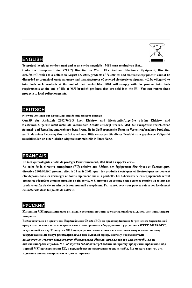
WEEE (Waste Electrical and Electronic Equipment) Statement
v
vi
vii

CONTENTS
Copyright Notice.........................................................................................................ii
Trademarks..................................................................................................................ii
Revision History.........................................................................................................ii
Technical Support......................................................................................................ii
Safety Instructions...................................................................................................iii
FCC-B Radio Frequency Interference Statement.............................................iv
WEEE (Waste Electrical and Electronic Equipment) Statement.......................v
English......................................................................................................................En-1
Mainboard Specifications.................................................................................En-2
Quick Components Guide..................................................................................En-4
CPU (Central Processing Unit)..........................................................................En-5
Memory...............................................................................................................En-9
Power Supply...................................................................................................En-11
Back Panel........................................................................................................En-12
Connectors......................................................................................................En-14
Buttons.............................................................................................................En-21
Switch..............................................................................................................En-22
Slots..................................................................................................................En-23
LED Status Indicators......................................................................................En-25
BIOS Setup.......................................................................................................En-26
Software Information......................................................................................En-36
Deutsch....................................................................................................................De-1
Spezifikationen..................................................................................................De-2
Komponenten-Übersicht...................................................................................De-4
CPU (Central Processing Unit)..........................................................................De-5
Speicher.............................................................................................................De-9
Stromversorgung............................................................................................De-11
Rücktafel..........................................................................................................De-12
Anschlüsse......................................................................................................De-14
Tasten...............................................................................................................De-21
Switch..............................................................................................................De-22
Steckplätze......................................................................................................De-23
LED Statusdikatoren........................................................................................De-25
BIOS Setup.......................................................................................................De-26
Software-Information......................................................................................De-36
viii

Français.....................................................................................................................Fr-1
Spécifications de la Carte Mère........................................................................Fr-2
Guide rapide des composants..........................................................................Fr-4
Processeur : CPU...............................................................................................Fr-5
Mémoire...............................................................................................................Fr-9
Connecteur d’alimentation...............................................................................Fr-11
Panneau arrière................................................................................................Fr-12
Connecteurs.....................................................................................................Fr-14
Boutons.............................................................................................................Fr-21
Interrupteur.......................................................................................................Fr-22
Slots...................................................................................................................Fr-23
Indicateurs de statuts de LED.........................................................................Fr-25
Réglages BIOS..................................................................................................Fr-26
Information de Logiciel.....................................................................................Fr-36
Русский ....................................................................................................................Ru-1
Характеристики ...............................................................................................Ru-2
Руководство по размещению компонентов ..............................................Ru-4
CPU (Центральный процессор).....................................................................Ru-5
Память ..............................................................................................................Ru-9
Разъем питания .............................................................................................Ru-11
Задняя панель ...............................................................................................Ru-12
Разъемы ..........................................................................................................Ru-14
Кнопки .............................................................................................................Ru-21
Переключатели ..............................................................................................Ru-22
Слоты ...............................................................................................................Ru-23
Световые индикаторы .................................................................................Ru-25
Настройка BIOS..............................................................................................Ru-26
Сведения о программном обеспечении ...................................................Ru-36
ix

P45 Neo2 /
P43 Neo2 Series
User’s Guide
Engli sh
English
En-1
MS-7558 Mainboard
Mainboard Specifications
Processor Support
- Intel® Core 2 Extreme, Core 2 Quad, Core 2 Duo, Pentium Dual-Core
and Celeron Dual-Core processors in the LGA775 package
- Intel® next generation 45 nm Multi-core CPU
(For the latest information about CPU, please visit http://global.
msi.com.tw/index.php?func=cpuform)
Supported FSB
- 1600*(OC)/ 1333/ 1066/ 800 MHz
Chipset
- North Bridge: Intel® P45/P43 chipset
- South Bridge: Intel® ICH10/ICH10R chipset
Memory Support
- 4 DDR2 DIMMs support DDR2 1066**(OC)/ 800/ 667 SDRAM
(240pin / 1.8V / 16GB Max)
(For more information on compatible components, please visit http:/
/global.msi.com.tw/index.php?func=testreport)
LAN
- Supports PCIE Single or Dual LAN 10/100/1000 Fast Ethernet by
Realtek 8111C
Audio
- Chip integrated by Realtek® ALC888
- Flexible 8-channel audio with jack sensing
- Compliant with Azalia 1.0 Spec
- Meet Microsoft Vista Premium spec
IDE
- 1 IDE port by JMicron JMB 363
- Supports Ultra DMA 66/100/133 mode
- Supports PIO, Bus Master operation mode
SATA
- 6 SATAII ports by ICH10/ICH10R (SATA1~6)
- 2 SATAII ports by JMicron JMB363 (SATA7~8)
- Supports storage and data transfers at up to 3 Gb/s
RAID
- Supports Intel Martix Storage Technology (AHCI + RAID 0/1/5/10) by
ICH10R
- Supports RAID 0, RAID 1 and JBOD by JMicron 363
1394 (optional)
- Supports 1394 by JMicron JMB381
FDD
- 1 floppy port
- Supports 1 FDD with 360KB, 720KB, 1.2MB, 1.44MB and 2.88MB
En-2
Connectors
Back panel
- 1 PS/2 mouse port
- 1 PS/2 keyboard port
- 1 Serial port (COM1)
- 6 USB 2.0 Ports
- 1 LAN jack or 2 LAN jacks
- 6 flexible audio jacks
- 1 1394 port (optional)
On-Board Pinheaders / Connectors
- 3 USB 2.0 pinheaders
- 1 1394 pinheader (optional)
- 1 chassis intrusion connector
- 1 SPDIF-out pinheader
- 1 CD-in connector
- 1 front audio pinheader
- 1 TPM Module connector
- 1 Hardware Overclock FSB Switch
- 1 Reset button
- 1 Power button
- 1 Clear CMOS button
Slots
- 2 PCI Express x16 slots
- 2 PCI Express x1 slots
- 2 PCI slots, support 3.3V/ 5V PCI bus Interface
Form Factor
- ATX (30.5cm X 24.4cm)
Mounting
- 9 mounting holes
Engli sh
En-3
MS-7558 Mainboard
ON
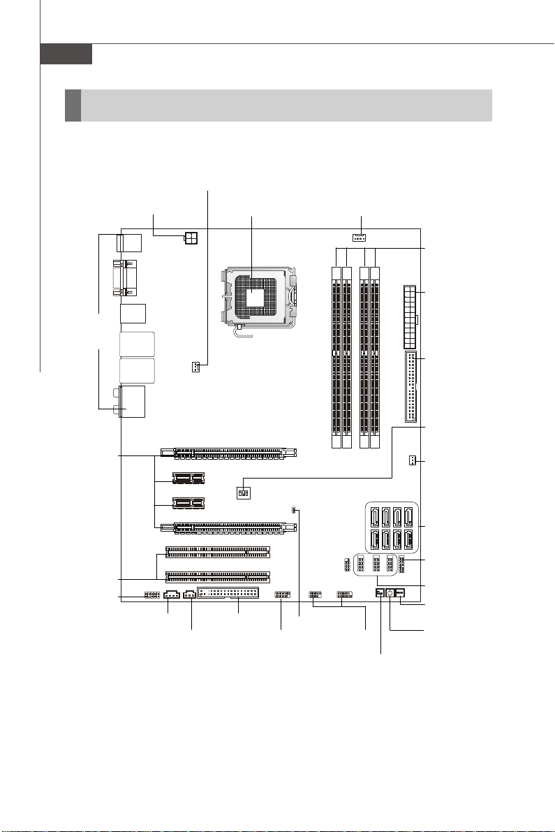
Quick Components Guide
SYSFAN2,
En-16
Back Panel,
En-12
PCIE,
En-23
PCI,
En-23
JAUD1,
En-19
JPWR2, En-11
JCD1,
En-18
JSP1,
En-17
CPU, En-5
123
FDD1,
En-14
JCI1, En-16
J1394_1,
En-17
CPUFAN1, En-16
JFP2, JFP1
En-18
CLR_CMOS1,
En-21
DDR2 DIMMs,
En-9
JPWR1,
En-11
IDE1,
En-14
OC_SW1,
En-22
SYSFAN1,
En-16
SATA,
En-15
JTPM1,
En-19
JUSB1~3,
En-20
RESET1,
En-21
POWRE1,
En-21
En-4
CPU (Central Processing Unit)
When you are installing the CPU, make sure to install the cooler to prevent
overheating. If you do not have the CPU cooler, consult your dealer before turning
on the computer.
For the latest information about CPU, please visit http://global.msi.com.tw/index.php?
func=cpuform
Important
Overheating
Overheating will seriously damage the CPU and system. Always make sure
the cooling fan can work properly to protect the CPU from overheating. Make
sure that you apply an even layer of thermal paste (or thermal tape) between
the CPU and the heatsink to enhance heat dissipation.
Replacing the CPU
While replacing the CPU, always turn off the ATX power supply or unplug the
power supply’s power cord from the grounded outlet first to ensure the safety
of CPU.
Overclocking
This mainboard is designed to support overclocking. However, please make
sure your components are able to tolerate such abnormal setting, while
doing overclocking. Any attempt to operate beyond product specifications is
not recommended. We do not guarantee the damages or risks caused
by inadequate operation or beyond product specifications.
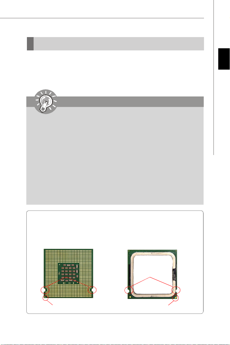
Introduction to LGA 775 CPU
The pin-pad side of LGA 775
CPU.
The surface of LGA 775 CPU.
Remember to apply some thermal paste on it for better heat
dispersion.
Engli sh
Alignment Key Alignment Key
Yellow triangle is the Pin 1 indicator
Yellow triangle is the Pin 1 indicator
En-5
MS-7558 Mainboard
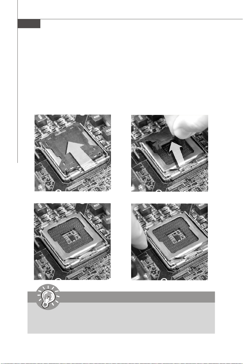
CPU & Cooler Installation
When you are installing the CPU, make sure the CPU has a cooler attached on
the top to prevent overheating. Meanwhile, do not forget to apply some thermal
paste on CPU before installing the heat sink/cooler fan for better heat dispersion.
Follow the steps below to install the CPU & cooler correctly. Wrong installation will
cause the damage of your CPU & mainboard.
1.The CPU socket has a plastic cap on
it to protect the contact from damage.
Before you install the CPU, always
cover it to protect the socket pin.
3.The pins of socket reveal.
2.Remove the cap from lever hinge
side (as the arrow shows).
4.Open the load lever.
Important
1.Confirm if your CPU cooler is firmly installed before turning on your system.
2. Do not touch the CPU socket pins to avoid damaging.
3. The availability of the CPU land side cover depends on your CPU packing.
En-6
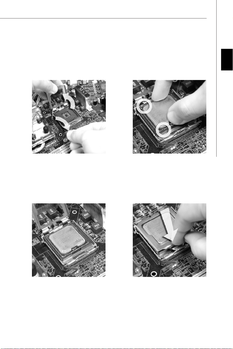
5.Lift the load lever up and open the
load plate.
6.After confirming the CPU direction
for correct mating, put down the
CPU in the socket housing frame.
Be sure to grasp on the edge of
the CPU base. Note that the alignment keys are matched.
alignment
key
Engli sh
7.Visually inspect if the CPU is
seated well into the socket. If not,
take out the CPU with pure vertical
motion and reinstall.
8.Cover the load plate onto the
package.
En-7
MS-7558 Mainboard
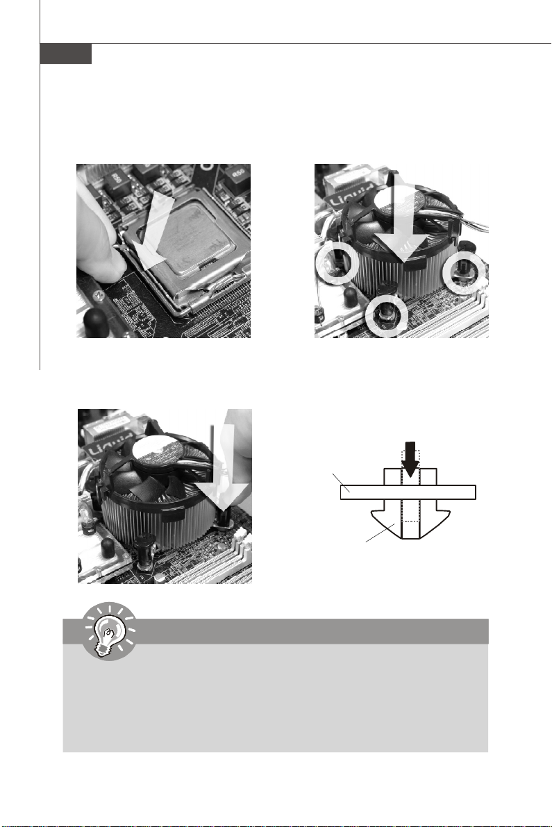
9.Press down the load lever lightly
onto the load plate, and then secure the lever with the hook under
retention tab.
11.Press the four hooks down to fasten
the cooler. Then rotate the locking
switch (refer to the correct direction
marked on it) to lock the hooks.
10. Align the holes on the mainboard
with the heatsink. Push down the
cooler until its four clips get
wedged into the holes of the
mainboard.
12.Turn over the mainboard to confirm that the clip-ends are correctly
inserted.
Mainboard
locking
switch
Hook
Important
1. Read the CPU status in BIOS.
2. Whenever CPU is not installed, always protect your CPU socket pin with the
plastic cap covered (shown in Figure 1) to avoid damaging.
3. Mainboard photos shown in this section are for demonstration of the CPU/
cooler installation only. The appearance of your mainboard may vary depending on the model you purchase.
En-8
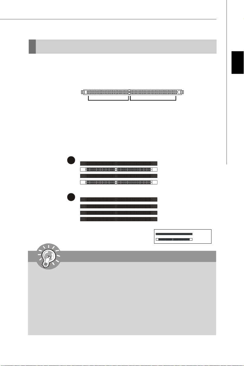
Memory
1
2
Installed
These DIMM slots are used for installing memory modules.
For more information on compatible components, please visit http://global.msi.com.
tw/index.php?func=testreport
DDR2
240-pin, 1.8V
64x2=128 pin56x2=112 pin
Dual-Channel Memory Population Rules
In Dual-Channel mode, the memory modules can transmit and receive data with two
data bus lines simultaneously. Enabling Dual-Channel mode can enhance the system
performance. Please refer to the following illustrations for population rules under
Dual-Channel mode.
DIMM1
DIMM2
DIMM3
DIMM4
DIMM1
DIMM2
DIMM3
DIMM4
Engli sh
Empty
Important
-DDR2 memory modules are not interchangeable with DDR and the DDR2
standard is not backwards compatible. You should always install DDR2
memory modules in the DDR2 DIMM slots.
-In Dual-Channel mode, make sure that you install memory modules of the
same type and density in different channel DIMM slots.
-To enable successful system boot-up, always insert the memory modules
into the DIMM1 first.
- Due to the chipset resource deployment, the system density will only be
detected up to 15+GB (not full 16GB) when each DIMM is installed with a 4GB
memory module.
En-9
MS-7558 Mainboard
Installing Memory Modules
1. The memory module has only one notch on the center and will only fit in the right
orientation.
2. Insert the memory module vertically into the DIMM slot. Then push it in until the
golden finger on the memory module is deeply inserted in the DIMM slot. The plastic
clip at each side of the DIMM slot will automatically close when the memory module
is properly seated.
Important
You can barely see the golden finger if the memory module is properly inserted
in the DIMM slot.
3. Manually check if the memory module has been locked in place by the DIMM slot
clips at the sides.
En-10
Volt
Notch
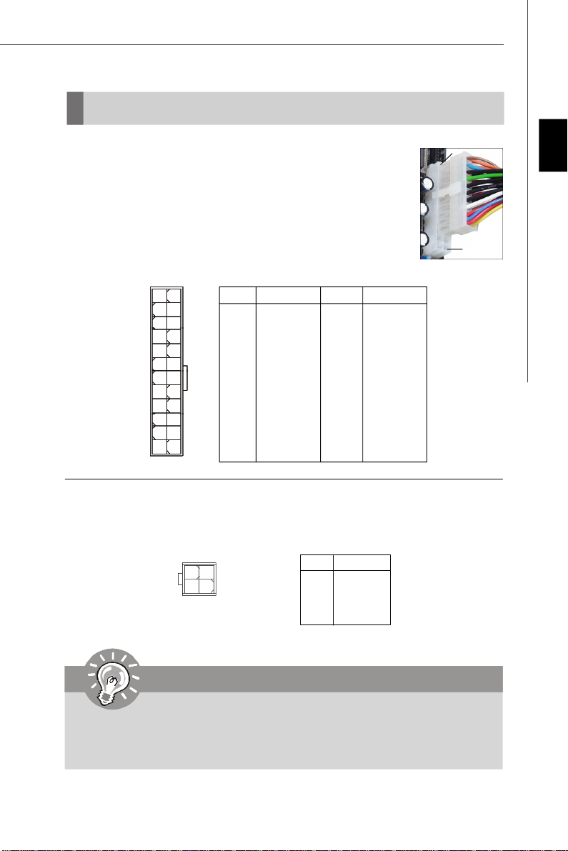
Power Supply
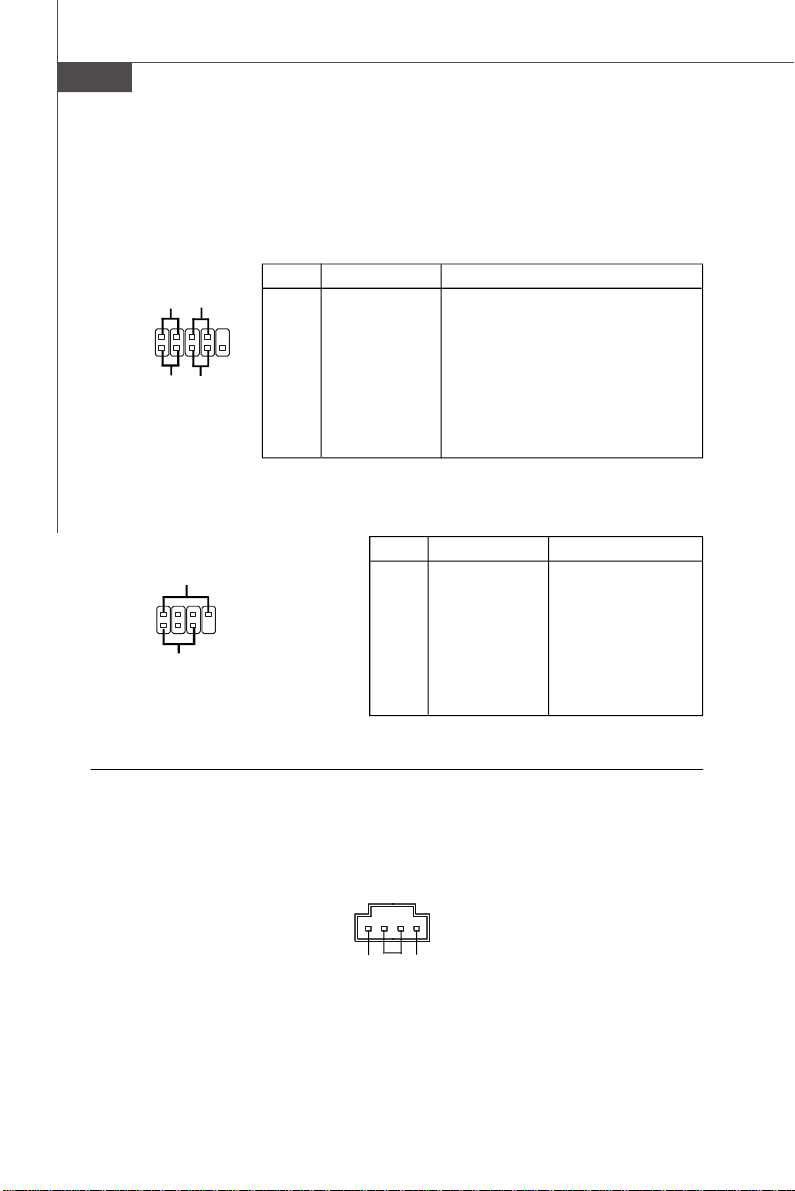
ATX 24-Pin Power Connector: JPWR1
This connector allows you to connect an ATX 24-pin power supply.
To connect the ATX 24-pin power supply, make sure the plug of the
power supply is inserted in the proper orientation and the pins are
aligned. Then push down the power supply firmly into the connector.
You may use the 20-pin ATX power supply as you like. If you’d like
to use the 20-pin ATX power supply, please plug your power supply along with pin 1 & pin 13 (refer to the image at the right hand).
Pin Definition
PIN SIGNAL
13 +3.3V
14 -12V
15 GND
16 PS-ON#
17 GND
18 GND
19 GND
20 Res
21 +5V
22 +5V
23 +5V
24 GND
JPWR1
12
1
24
13
PIN SIGNAL
1 +3.3V
2 +3.3V
3 GND
4 +5V
5 GND
6 +5V
7 GND
8 PWR OK
9 5VSB
10 +12V
11 +12V
12 +3.3V
ATX 4-pin Power Connector: JPWR2
This power connector is used to provide power to the CPU.
4 2
JPWR2
13
Pin Definition
PIN SIGNAL
1 GND
2 GND
3 12V
4 12V
pin 13
pin 12
English
Important
1. Make sure that all the connectors are connected to proper ATX power supplies to ensure stable operation of the mainboard.
2. Power supply of 400 watts (and above) is highly recommended for system
stability.
En-11
MS-7558 Mainboard
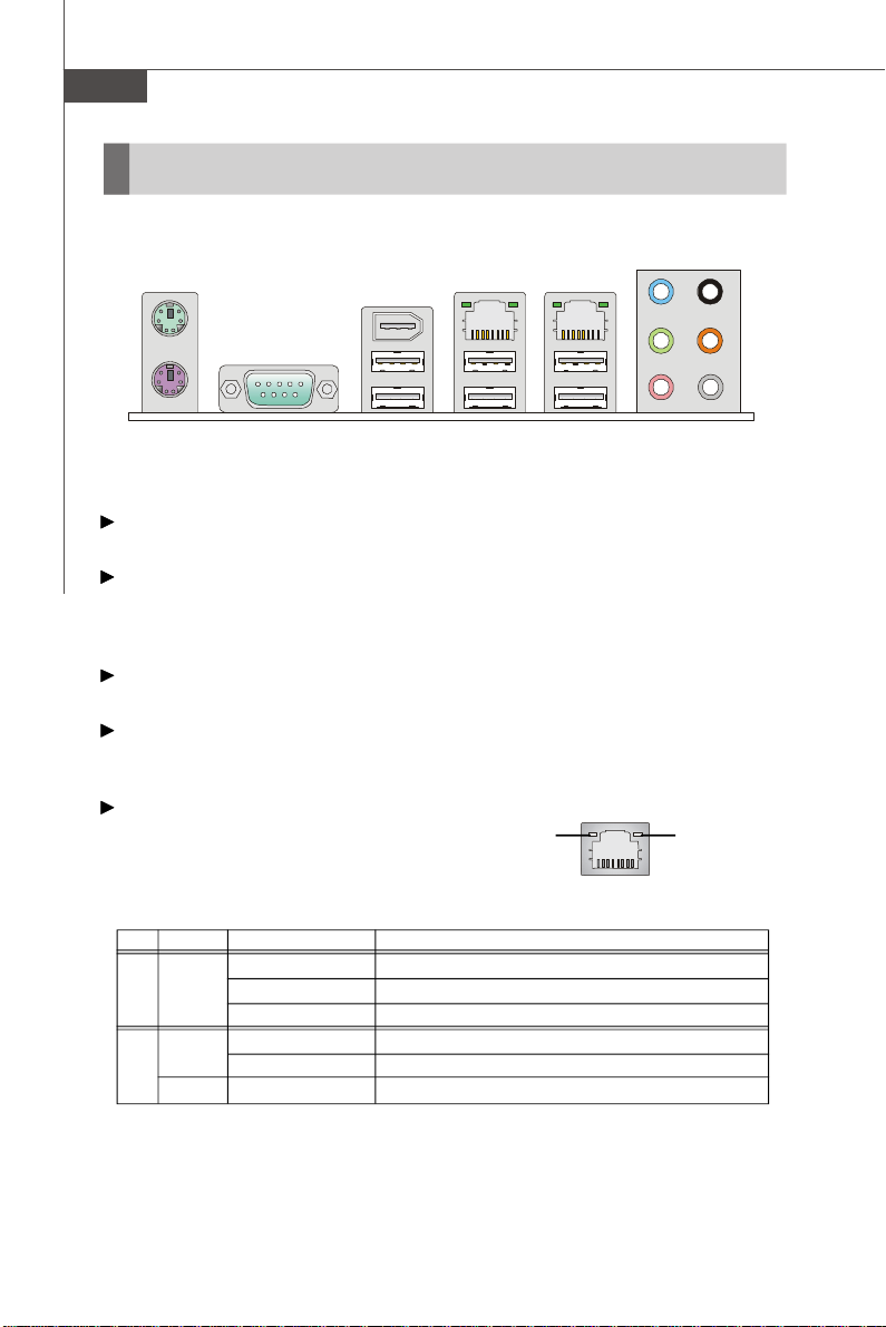
Back Panel
Mouse
Keyboard Mic
Serial Port
1394 Port
(optional)
USB Port
LAN
(optional)
USB Port USB Port
LAN
Line-In
Line-Out
RS-Out
CS-Out
SS-Out
Mouse/Keyboard
The standard PS/2® mouse/keyboard DIN connector is for a PS/2® mouse/keyboard.
Serial Port
The serial port is a 16550A high speed communications port that sends/ receives 16
bytes FIFOs. You can attach a serial mouse or other serial devices directly to the
connector.
1394 Port (optional)
The IEEE1394 port on the back panel provides connection to IEEE1394 devices.
USB Port
The USB (Universal Serial Bus) port is for attaching USB devices such as keyboard,
mouse, or other USB-compatible devices.
LAN
The standard RJ-45 LAN jack is for connection to
Green / OrangeYellow
the Local Area Network (LAN). You can connect a
network cable to it.
LED Color LED State Condition
Off LAN link is not established.
Left Yellow On (steady state) LAN link is established.
On (brighter & pulsing)The computer is communicating with another computer on the LAN.
Green Off 10 Mbit/sec data rate is selected.
Right On 100 Mbit/sec data rate is selected.
Orange On 1000 Mbit/sec data rate is selected.
En-12

Audio Ports
These audio connectors are used for audio devices. It is easy to differentiate between audio effects according to the color of audio jacks.
Line-In (Blue) - Line In is used for external CD player, tapeplayer or
other audio devices.
Line-Out (Green) - Line Out, is a connector for speakers or headphones.
Mic (Pink) - Mic, is a connector for microphones.
RS-Out (Black) - Rear-Surround Out in 4/ 5.1/ 7.1 channel mode.
CS-Out (Orange) - Center/ Subwoofer Out in 5.1/ 7.1 channel mode.
SS-Out (Gray) - Side-Surround Out 7.1 channel mode.
English
En-13
MS-7558 Mainboard
Connectors
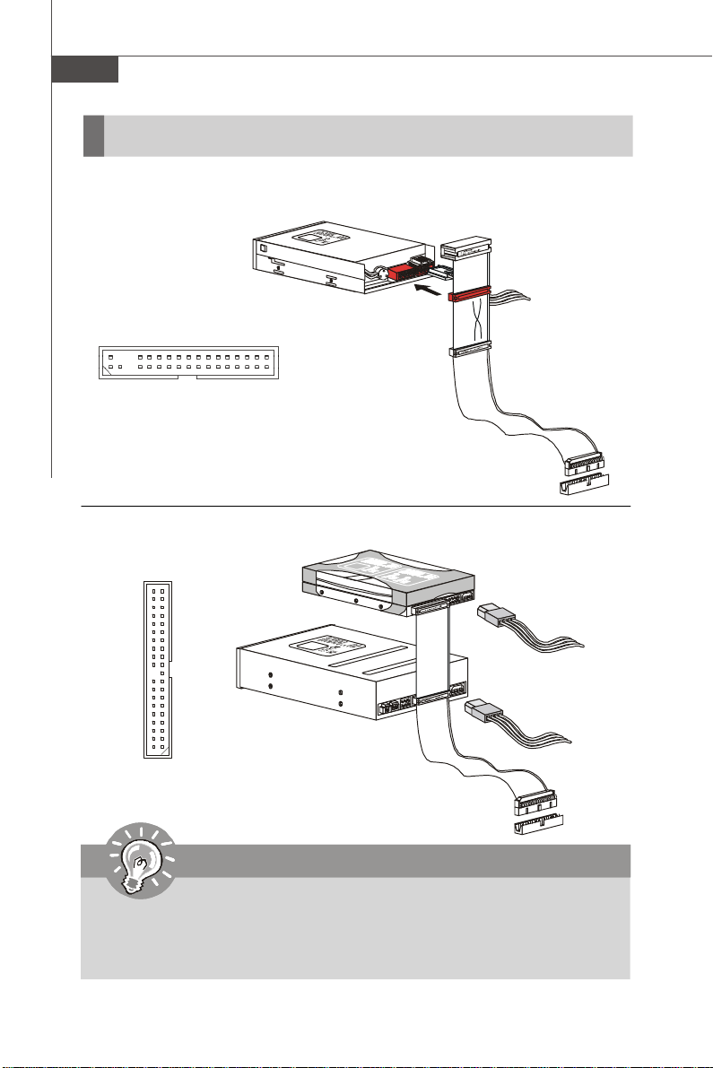
Floppy Disk Drive Connector: FDD1
This connector supports 360KB, 720KB, 1.2MB, 1.44MB or 2.88MB floppy disk drive.
IDE Connector: IDE1
This connector supports IDE hard disk drives, optical disk drives and other IDE devices.
Important
If you install two IDE devices on the same cable, you must configure the
drives separately to master / slave mode by setting jumpers. Refer to IDE
device’s documentation supplied by the vendors for jumper setting
instructions.
En-14
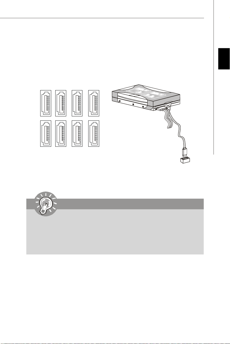
Serial ATA Connector: SATA1~8
This connector is a high-speed Serial ATA interface port. Each connector can connect
to one Serial ATA device.
English
SATA6 SATA2
SATA5
SATA4
SATA3
SATA1
SATA8
SATA7
Important
1. Please do not fold the Serial ATA cable into 90-degree angle. Otherwise,
data loss may occur during transmission.
2. SATA1~6 controlled by ICH10/ICH10R, and ICH10R supports RAID 0/ 1/ 5/
10 mode.
3. SATA7~8 controlled by JMB 363 and they support RAID 0/ 1 and JBOD
mode.
En-15
MS-7558 Mainboard
Fan Power Connectors: CPUFAN1, SYSFAN1/2
The fan power connectors support system cooling fan with +12V. When connecting
the wire to the connectors, always note that the red wire is the positive and should
be connected to the +12V; the black wire is Ground and should be connected to GND.
If the mainboard has a System Hardware Monitor chipset on-board, you must use a
specially designed fan with speed sensor to take advantage of the CPU fan control.
SENSOR
+12V
GND
CONTROL
CPUFAN1
SENSOR
+12V
GND
SYSFAN1/2
Important
1.Please refer to the recommended CPU fans at processor’s official website
or consult the vendors for proper CPU cooling fan.
2.CPUFAN supports fan control. You can install Dual Core Center utility that
will automatically control the CPU fan speed according to the actual CPU
temperature.
3. Fan cooler set with 3 or 4 pins power connector are both available for
CPUFAN1.
Chassis Intrusion Connector: JCI1
This connector connects to the chassis intrusion switch cable. If the chassis is
opened, the chassis intrusion mechanism will be activated. The system will record
this status and show a warning message on the screen. To clear the warning, you
must enter the BIOS utility and clear the record.
GND
2
1
CINTRU
JCI1
En-16
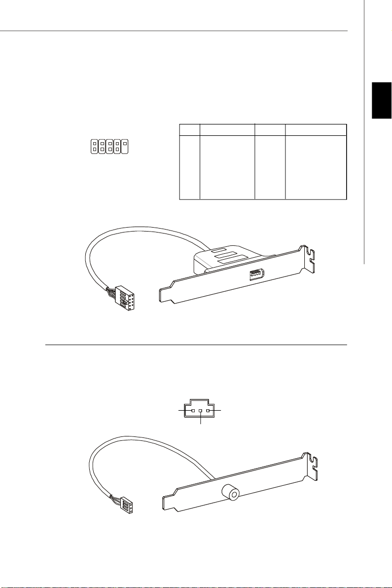
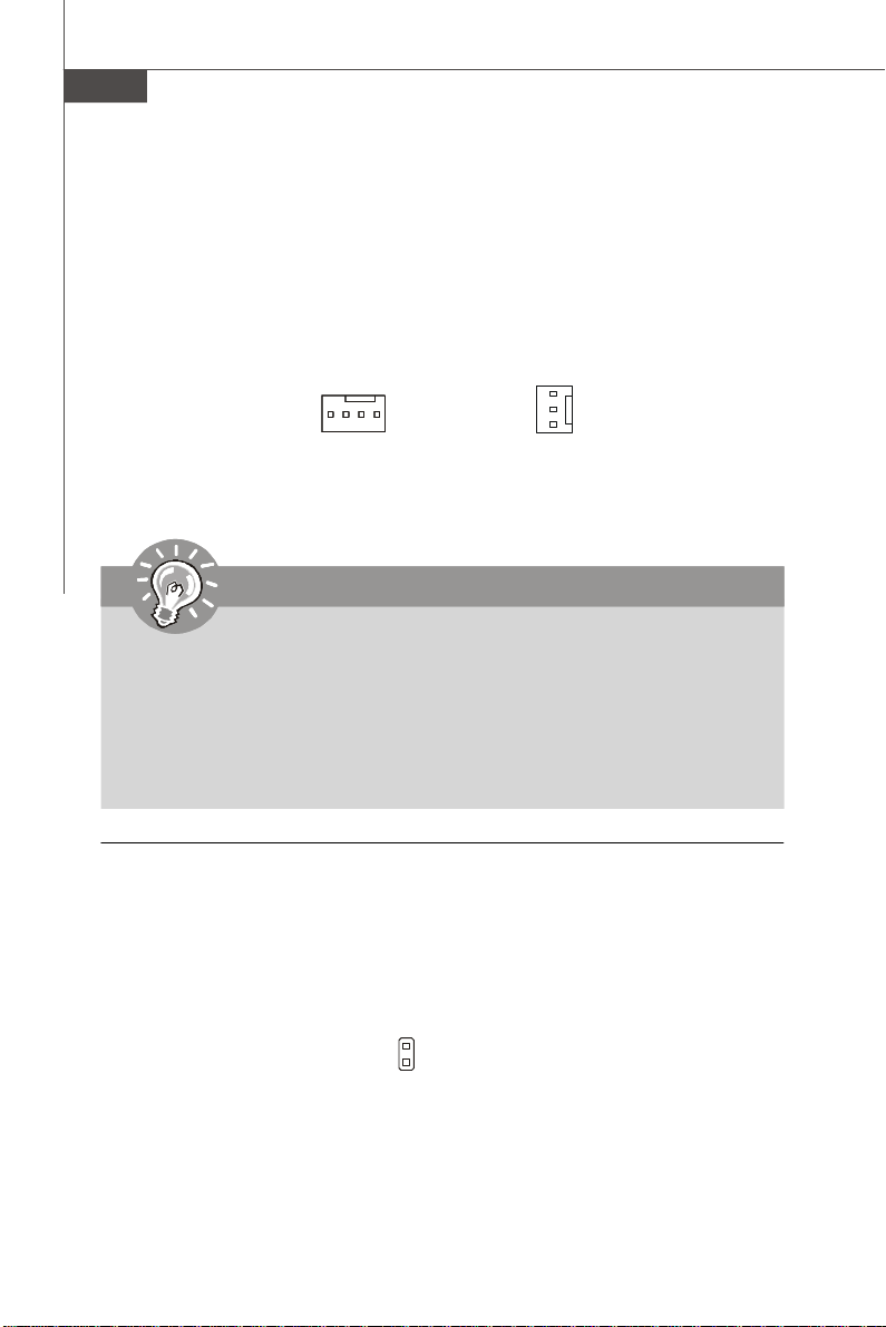
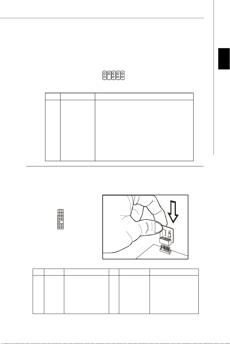
IEEE1394 Connector: J1394_1 (optional)
This connector allows you to connect the IEEE1394 device via an optional IEEE1394
bracket.
Pin Definition
PIN SIGNAL PIN SIGNAL
2
1
J1394_1
10
9
1 TPA+ 2 TPA-
3 Ground 4 Ground
5 TPB+ 6 TPB-
7 Cable power 8 Cable power
9 Key (no pin) 10 Ground
IEEE1394 Bracket (optional)
S/PDIF-Out Connector: JSP1
This connector is used to connect S/PDIF (Sony & Philips Digital Interconnect Format)
interface for digital audio transmission.
JSP1
English
VCC
GND
SPDIF
S/PDIF Bracket (optional)
En-17
MS-7558 Mainboard
Front Panel Connectors: JFP1, JFP2
These connectors are for electrical connection to the front panel switches and LEDs.
The JFP1 is compliant with Intel® Front Panel I/O Connectivity Design Guide.
JFP1 Pin Definition
PIN SIGNAL DESCRIPTION
1 HD_LED + Hard disk LED pull-up
2 FP PWR/SLP MSG LED pull-up
10
3 HD_LED - Hard disk active LED
9
4 FP PWR/SLP MSG LED pull-up
5 RST_SW - Reset Switch low reference pull-down to GND
6 PWR_SW + Power Switch high reference pull-up
7 RST_SW + Reset Switch high reference pull-up
8 PWR_SW - Power Switch low reference pull-down to GND
9 RSVD_DNU Reserved. Do not use.
JFP2 Pin Definition
PIN SIGNAL DESCRIPTION
1 GND Ground
2 SPK- Speaker-
8
7
3 SLED Suspend LED
4 BUZ+ Buzzer+
5 PLED Power LED
6 BUZ- Buzzer-
7 NC No connection
8 SPK+ Speaker+
JFP1
JFP2
Power
LED
2
1
2
1
-
+
HDD
LED
Speaker
+
Power
LED
Power
Switch
-
+
-
+
Reset
Switch
+
-
CD-In Connector: JCD1
This connector is provided for external audio input.
JCD1
R
L
GND
En-18
Front Panel Audio Connector: JAUD1
This connector allows you to connect the front panel audio and is compliant with
Intel® Front Panel I/O Connectivity Design Guide.
JAUD1
9
10
HD Audio Pin Definition
PIN SIGNAL DESCRIPTION
1 MIC_L Microphone - Left channel
2 GND Ground
3 MIC_R Microphone - Right channel
4 NC
5 LINE out_R Analog Port - Right channel
6 MIC_JD Jack detection return from front panel microphone JACK1
7 Front_JD Jack detection sense line from the High Definition Audio CODEC
8 NC No control
9 LINE out_L Analog Port - Left channel
10 LINEout_JD Jack detection return from front panel JACK2
jack detection resistor network
1
2
TPM Module Connector: JTPM1
This connector connects to a TPM (Trusted Platform Module) module (optional). Please
refer to the TPM security platform manual for more details and usages.
2
1
English
1413
Pin Signal Description Pin Signal Description
1 LCLK LPC clock 2 3V_STB 3V standby power
3 LRST# LPC reset 4 VCC3 3.3V power
5 LAD0 LPC address & data pin0 6 SIRQ Serial IRQ
7 LAD1 LPC address & data pin1 8 VCC5 5V power
9 LAD2 LPC address & data pin2 10 KEY No pin
11 LAD3 LPC address & data pin3 12 GND Ground
13 LFRAME# LPC Frame 14 GND Ground
En-19
MS-7558 Mainboard
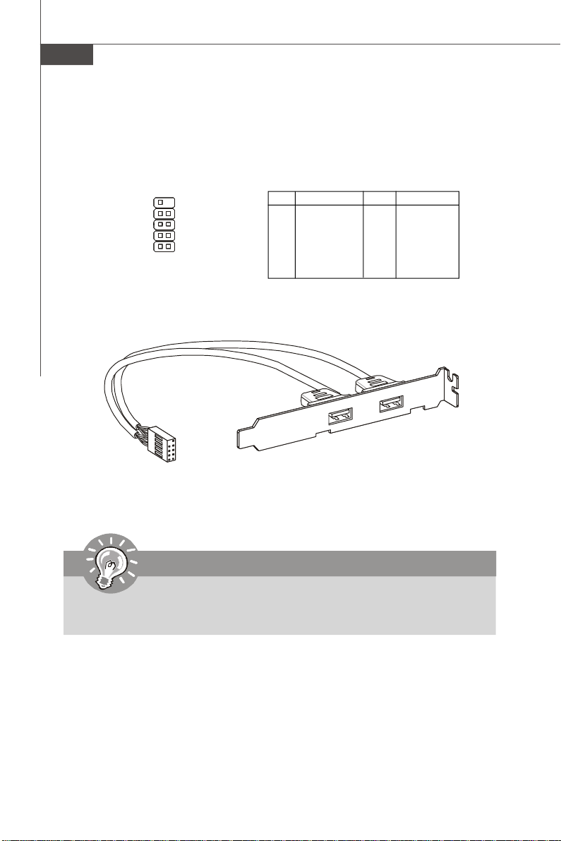
Front USB Connector: JUSB1~3
These connectors, compliant with Intel® I/O Connectivity Design Guide, is ideal for
connecting high-speed USB interface peripherals such as USB HDD, digital cameras,
MP3 players, printers, modems and the like.
Pin Definition
10 9
1 2
JUSB1~3
PIN SIGNAL PIN SIGNAL
1 VCC 2 VCC
3 USB0- 4 USB1-
5 USB0+ 6 USB1+
7 GND 8 GND
9 Key (no pin) 10 NC
USB 2.0 Bracket
(optional)
Important
Note that the pins of VCC and GND must be connected correctly to avoid
possible damage.
En-20
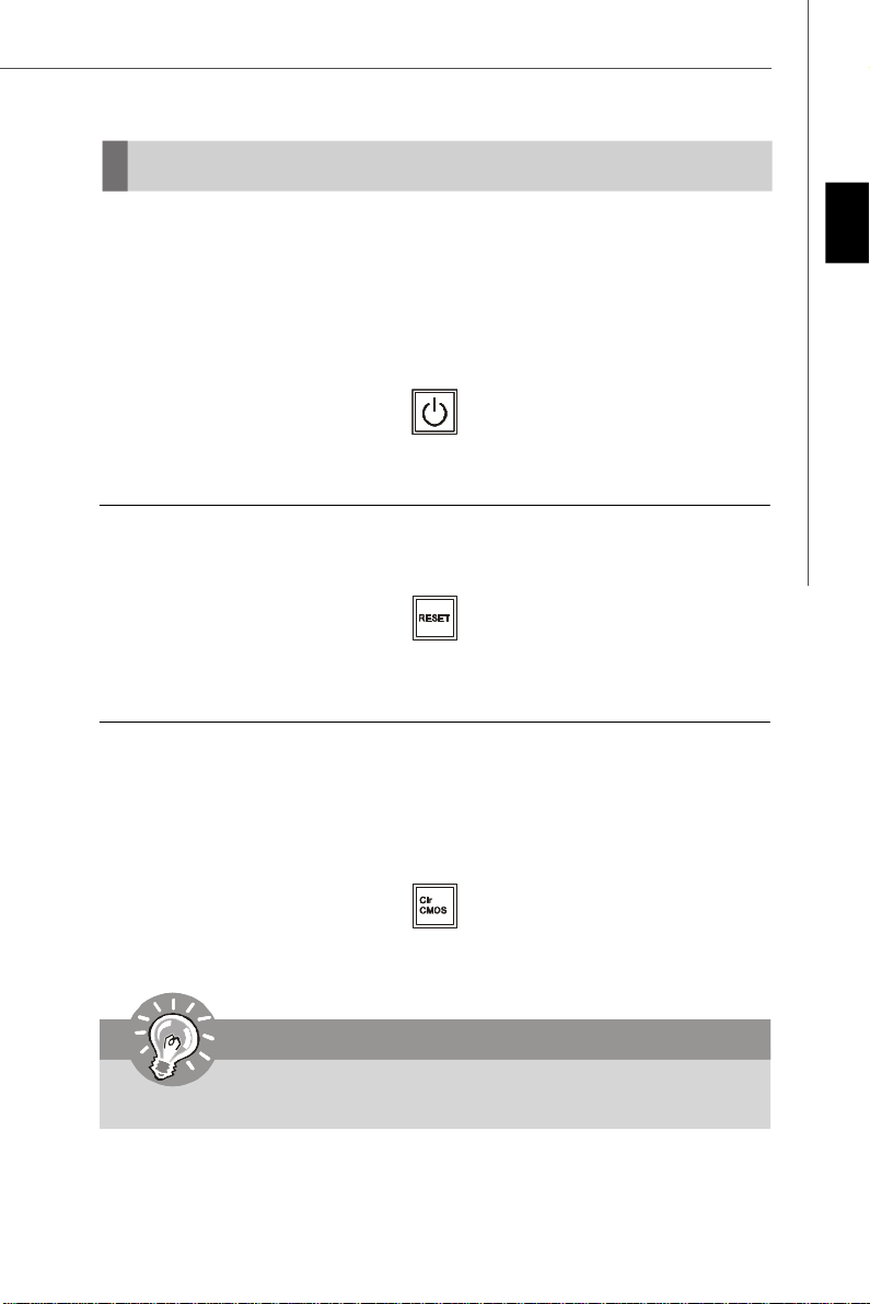
Buttons
The motherboard provides the following buttons(optinoal) for you to set the computer’s
function. This section will explain how to change your motherboard’s function through
the use of button.
Power Button: POWER1
This power button is used to turn-on or turn-off the system. Press the button to turnon or turn-off the system.
POWER1
Reset Button: RESET1
This reset button is used to reset the system. Press the button to reset the system.
RESET1
Clear CMOS Button: CLR_CMOS1
There is a CMOS RAM onboard that has a power supply from an external battery to
keep the data of system configuration. With the CMOS RAM, the system can automatically boot OS every time it is turned on. If you want to clear the system configuration,
simply press the button to clear data.
English
CLR_CMOS1
Important
Make sure that you power off the system before press the clear CMOS button.
En-21

MS-7558 Mainboard
Switch
Hardware Overclock FSB Switch: OC_SW1
You can overclock the FSB to increase the processor frequency by changing the
switch OC_SW1. Follow the instructions below to set the FSB.
ON
123
Default
ON
123
200->266 MHz 200->333 MHz 200->400 MHz
ON
123
ON
123
266->333 MHz
ON
123
266->400 MHz
333->400 MHz
Important
1. Make sure that you power off the system before changing the switch.
2. Overclocking may cause instability or crash during boot, then please set
the switch to default setting.
En-22

Slots
PCI (Peripheral Component Interconnect) Express Slot
The PCI Express slot supports the PCI Express interface expansion card.
The PCI Express 2.0x 16 supports up to 8.0 GB/s transfer rate.
The PCI Express x 1 supports up to 250 MB/s transfer rate.
PCI Express x16 Slot
PCI Express x 1 Slot
PCI (Peripheral Component Interconnect) Slot
The PCI slot supports LAN card, SCSI card, USB card, and other add-on cards that
comply with PCI specifications.
32-bit PCI Slot
English
Important
When adding or removing expansion cards, make sure that you unplug the
power supply first. Meanwhile, read the documentation for the expansion card
to configure any necessary hardware or software settings for the expansion
card, such as jumpers, switches or BIOS configuration.
En-23

MS-7558 Mainboard
PCI Interrupt Request Routing
The IRQ, acronym of interrupt request line and pronounced I-R-Q, are hardware lines
over which devices can send interrupt signals to the microprocessor. The PCI IRQ
pins are typically connected to the PCI bus pins as follows:
Order 1 Order 2 Order 3 Order 4
PCI Slot 1 INT A# INT B# INT C# INT D#
PCI Slot 2 INT E# INT F# INT G# INT H#
En-24

LED Status Indicators
3
LED4
LED1
LED2
1 2
ON
LED3
English
Blue Light Off
LED1 LED2 LED3 LED4 Mode
CPU is in 1 phase power mode.
CPU is in 2 phase power mode.
CPU is in 3 phase power mode.
CPU is in 4 phase power mode.
En-25

MS-7558 Mainboard
BIOS Setup
This chapter provides basic information on the BIOS Setup program and allows you to
configure the system for optimum use. You may need to run the Setup program
when:
* An error message appears on the screen during the system booting up, and requests you to run BIOS SETUP.
* You want to change the default settings for customized features.
Important
1.The items under each BIOS category described in this chapter are under
continuous update for better system performance. Therefore, the description
may be slightly different from the latest BIOS and should be held for reference
only.
2.Upon boot-up, the 1st line appearing after the memory count is the BIOS
version. It is usually in the format:
1st digit refers to BIOS maker as A = AMI, W = AWARD, and P = PHOENIX.
2nd - 5th digit refers to the model number.
6th refers to the Chipset vender as A = AMD, I = Intel, V = VIA, N = Nvidia, U =
ULi.
7th - 8th digit refers to the customer as MS = all standard customers.
V1.1 refers to the BIOS version.
082208 refers to the date this BIOS was released.
A7558IMS V1.1 082208 where:
En-26

Entering Setup
Power on the computer and the system will start POST (Power On Self Test) process.
When the message below appears on the screen, press <DEL> key to enter Setup.
Press DEL to enter SETUP
If the message disappears before you respond and you still wish to enter Setup,
restart the system by turning it OFF and On or pressing the RESET button. You may
also restart the system by simultaneously pressing <Ctrl>, <Alt>, and <Delete> keys.
Getting Help
After entering the Setup menu, the first menu you will see is the Main Menu.
Main Menu
The main menu lists the setup functions you can make changes to. You can use the
arrow keys (↑↓ ) to select the item. The on-line description of the highlighted setup
function is displayed at the bottom of the screen.
Sub-Menu
If you find a right pointer symbol (as shown in the right view)
appears to the left of certain fields that means a sub-menu
containing additional options can be launched from this field.
You can use control keys (↑↓ ) to highlight the field and
press <Enter> to call up the sub-menu. Then you can use the control keys to enter
values and move from field to field within a sub-menu. If you want to return to the
main menu, just press <Esc >.
General Help <F1>
The BIOS setup program provides a General Help screen. You can call up this screen
from any menu by simply pressing <F1>. The Help screen lists the appropriate keys
to use and the possible selections for the highlighted item. Press <Esc> to exit the
Help screen.
English
En-27

MS-7558 Mainboard
The Main Menu
Once you enter AMI® or AWARD® BIOS CMOS Setup Utility, the Main Menu will appear
on the screen. The Main Menu allows you to select from ten setup functions and two
exit choices. Use arrow keys to select among the items and press <Enter> to accept
or enter the sub-menu.
Standard CMOS Features
Use this menu for basic system configurations, such as time, date etc.
Advanced BIOS Features
Use this menu to setup the items of special enhanced features.
Integrated Peripherals
Use this menu to specify your settings for integrated peripherals.
Power Management Setup
Use this menu to specify your settings for power management.
H/W Monitor
This entry shows your PC health status.
GreenPower
Use this menu to specify the power phase.
BIOS Setting Password
Use this menu to set the Password.
Cell Menu
Use this menu to specify your settings for frequency/voltage control and overclocking.
USER SETTINGS
Use this menu to save/ load your settings to/ from CMOS for BIOS.
Load Fail-Safe Defaults
Use this menu to load the default values set by the BIOS vendor for stable system
performance.
Load Optimized Defaults
Use this menu to load the default values set by the mainboard manufacturer specifically for optimal performance of the mainboard.
Save & Exit Setup
Save changes to CMOS and exit setup.
Exit Without Saving
Abandon all changes and exit setup.
En-28

When enter the BIOS Setup utility, follow the processes below for general use.
1. Load Optimized Defaults : Use control keys (↑↓) to highlight the Load Opti-
mized Defaults field and press <Enter> , a message as below appears:
Select [Ok] and press Enter to load the default settings for optimal system
performance.
2. Setup Date/ Time : Select the Standard CMOS Features and press <Enter> to
enter the Standard CMOS Features-menu. Adjust the Date, Time fields.
3. Save & Exit Setup : Use control keys (↑↓) to highlight the Save & Exit Setup
field and press <Enter> , a message as below appears:
English
Select [Ok] and press Enter to save the configurations and exit BIOS Setup utility.
Important
The configuration above are for general use only. If you need the detailed
settings of BIOS, please see the manual in English version on MSI website.
En-29

MS-7558 Mainboard
4. Cell Menu Introduction : This menu is for advanced user who want to overclock
the mainboard.
Important
Change these settings only if you are familiar with the chipset.
Current CPU / DRAM Frequency
These items show the current clocks of CPU and Memory speed. Read-only.
Multi-step OC Booster
This item is used to avoid the BIOS might crash with overclocking.
Disabled Disable this item, apply OC settings during POST.
Mode 1 Slight OC during POST and then apply full OC when loading
Mode 2 Load the OS then apply the OC settings.
En-30
the OS

D.O.T. Control
D.O.T. (Dynamic Overclocking Technology) is an automatic overclocking function,
included in the MSITM’s newly developed Dual CoreCell
TM
Technology. It is designed to
detect the load balance of CPU while running programs, and to adjust the best frequency automatically. When the mainboard detects system is running programs, it
will speed up automatically to make the program run smoothly and faster. When the
system is temporarily suspending or staying in the low load balance, it will restore the
default settings instead. Usually the Dynamic Overclocking Technology will be powered only when users' PC need to run huge amount of data like 3D games or the video
process, and the CPU and PCIE frequency need to be boosted up to enhance the
overall performance.
Important
Even though the Dynamic Overclocking Technology is more stable than
manual overclocking, basically, it is still risky. We suggest user to make
sure that your CPU / memory modules can afford to overclocking regularly
first. If you find the PC appears to be unstable or reboot incidentally, it's
better to disable the Dynamic Overclocking or to lower the level of
overclocking options. By the way, if you need to conduct overclocking
manually, you also need to disable the Dynamic OverClocking first.
Intel EIST
The Enhanced Intel SpeedStep technology allows you to set the performance level of
the microprocessor whether the computer is running on battery or AC power. This
field will appear after you installed the CPU which support speedstep technology.
English
Adjust CPU FSB Frequency (MHz)
This item allows you to set the CPU FSB frequency (in MHz).
Adjusted CPU Frequency (MHz)
It shows the adjusted CPU frequency (FSB x Ratio). Read-only.
Advance DRAM Configuration
Press <Enter> to enter the sub-menu and the following screen appears.
En-31

MS-7558 Mainboard
MEMORY-Z
Press <Enter> to enter the sub-menu and the following screen appears.
DIMM1~4 Memory SPD Infromation
Press <Enter> to enter the sub-menu and the following screen appears.
DIMM1~4 Memory SPD Infromation
These items display the current status of the current DIMM Memory speed
information such as memory type, max bandwidth, manufacture, part number,
serial number, SDRAM cycle time, DRAM TCL, DRAM TRCD, DRAM TRP, DRAM
TRAS, DRAM TRFC, DRAM TWR, DRAM TWTR, DRAM TRRD and DRAM TRTP.
They are read only.
CAS# Latency (CL)
This controls the CAS latency, which determines the timing delay (in clock cycles)
before SDRAM starts a read command after receiving it.
tRCD
When DRAM is refreshed, both rows and columns are addressed separately.
This setup item allows you to determine the timing of the transition from RAS
(row address strobe) to CAS (column address strobe). The less the clock
cycles, the faster the DRAM performance.
tRP
This setting controls the number of cycles for Row Address Strobe (RAS) to be
allowed to precharge. If insufficient time is allowed for the RAS to accumulate its
charge before DRAM refresh, refresh may be incomplete and DRAM may fail to
retain data. This item applies only when synchronous DRAM is installed in the
system.
En-32

tRAS
This setting determines the time RAS takes to read from and write to memory
cell.
1N/2N Memory Timing
This item controls the SDRAM command rate. Select [1N] makes SDRAM signal
controller to run at 1N (N=clock cycles) rate. Selecting [2N] makes SDRAM signal
controller run at 2N rate.
Advance Memory Setting
Setting to [Auto] enables the advance memory timing automatically to be determined by BIOS. Setting to [Manual] allows you to set advanced memory timings.
TRFC
When the Advance Memory Setting sets to [Manual], the field is adjustable.
This setting determines the time RFC takes to read from and write to a memory
cell.
TWR
When the Advance Memory Setting sets to [Manual], the field is adjustable.
Minimum time interval between end of write data burst and the start of a precharge
command. Allows sense amplifiers to restore data to cells.
TWTR
When the Advance Memory Setting sets to [Manual], the field is adjustable.
Minimum time interval between the end of write data burst and the start of a
column-read command. It allows I/O gating to overdrive sense amplifiers before
read command starts.
TRRD
When the Advance Memory Setting sets to [Manual], the field is adjustable.
Specifies the active-to-active delay of different banks.
English
TRTP
When the Advance Memory Setting sets to [Manual], the field is adjustable.
Time interval between a read and a precharge command.
CHA TRD/ TRD2RD/ TWR2WR/ TWR2RD/ /TWD2WR/ TRD Phase
When the Advance Memory Setting sets to [Manual], these fields are
adjustable. These items is used to set the memory timings for memory channel A.
CHB TRD/ TRD2RD/ TWR2WR/ TWR2RD/ TRD2WR/ TRD Phase
When the Advance Memory Setting sets to [Manual], these fields are
adjustable. These items is used to set the memory timings for memory channel B.
En-33

MS-7558 Mainboard
FSB/DRAM Ratio
This item will allow you to adjust the ratio of FSB to memory.
Adjusted DRAM Frequency (MHz)
It shows the adjusted DDR Memory frequency. Read-only.
ClockGen Tuner
Press <Enter> to enter the sub-menu.
CPU Clock Drive/ PCI Express Clock Drive
These items are used to select the CPU/ PCI Express clock amplitude.
CPU CLK Skew/ MCH CLK Skew
These items are used to select the CPU/ North Bridge chipset clock skew. They
can help CPU to reach the higher overclocking performace.
Adjust PCI Frequency (MHz)
This field allows you to select the PCI frequency (in MHz).
Auto Disable DRAM/PCI Frequency
When set to [Enabled], the system will remove (turn off) clocks from empty DIMM and
PCI slots to minimize the electromagnetic interference (EMI).
CPU Voltage (V)/ CPU GTL REF0 / CPU GTL REF1 / DRAM Voltage (V)/ MCH
Voltage (V)/ MCH GTL REF / VTT FSB Voltage (V)/ ICH Voltage (V)
These items are used to asjust the voltage of CPU, Memory, FSB and chipset.
Spread Spectrum
When the mainboard’s clock generator pulses, the extreme values (spikes) of the
pulses create EMI (Electromagnetic Interference). The Spread Spectrum function
reduces the EMI generated by modulating the pulses so that the spikes of the pulses
are reduced to flatter curves. If you do not have any EMI problem, leave the setting at
Disabled for optimal system stability and performance. But if you are plagued by EMI,
set to Enabled for EMI reduction. Remember to disable Spread Spectrum if you are
overclocking because even a slight jitter can introduce a temporary boost in clock
speed which may just cause your overclocked processor to lock up.
En-34

Important
1.If you do not have any EMI problem, leave the setting at [Disabled] for
optimal system stability and performance. But if you are plagued by EMI,
select the value of Spread Spectrum for EMI reduction.
2.The greater the Spread Spectrum value is, the greater the EMI is reduced,
and the system will become less stable. For the most suitable Spread
Spectrum value, please consult your local EMI regulation.
3.Remember to disable Spread Spectrum if you are overclocking because
even a slight jitter can introduce a temporary boost in clock speed which
may just cause your overclocked processor to lock up.
English
En-35

MS-7558 Mainboard
Software Information
Take out the Driver/Utility CD that is included in the mainboard package, and place it into
the CD-ROM drive. The installation will auto-run, simply click the driver or utility and
follow the pop-up screen to complete the installation. The Driver/Utility CD contains
the:
Driver menu - The Driver menu shows the available drivers. Install the driver by your
desire and to activate the device.
Utility menu - The Utility menu shows the software applications that the mainboard
supports.
WebSite menu- The WebSite menu shows the necessary websites.
Important
Please visit the MSI website to get the latest drivers and BIOS for better
system performance.
En-36

P45 Neo2 /
P43 Neo2 Serie
Benutzerhandbuch
Deutsch
Deutsch
De-1

MS-7558 Mainboard
Spezifikationen
Prozessoren
- Intel® Core 2 Extreme, Core 2 Quad, Core 2 Duo, Pentium Dual-Core
und Celeron Dual-Core Prozessoren für Sockel LGA775
- Intel® nächste Generation 45 nm Multi-Core CPU
(Weitere CPU Informationen finden Sie unter http://global.msi.com.
tw/index.php?func=cpuform)
FSB (Front-Side-Bus)
- 1600*(OC)/ 1333/ 1066/ 800 MHz
Chipsatz
- North-Bridge: Intel® P45/P43 Chipsatz
- South-Bridge: Intel® ICH10/ICH10R Chipsatz
Speicher
- 4 DDR2 DIMMs unterstützt DDR2 1066**(OC)/ 800/ 667 SDRAM
(240Pin / 1.8V / max. 16GB)
(Weitere Informationen zu kompatiblen Speichermodulen finden
Sie unter http://global.msi.com.tw/index.php?func=testreport)
LAN
- Unterstützt die PCIE Single oder Dual LAN 10/100/1000 Fast Ethernet
über Realtek 8111C
Audio
- Onboard Soundchip Realtek® ALC888
- 8-Kanal Audio-Ausgang mit “Jack Sensing” Funktion
- Erfüllt die Azalia Spezifikationen
- Zertifiziert für das Microsoft Vista Premium Betriebs-system
IDE
- 1 IDE Port über JMicron JMB 363
- Unterstützt die Betriebmodi mit Ultra DMA 66/100/133
- Unterstützt die Betriebmodi mit PIO, Bus Mastering
SATA
- 6 SATAII Ports über ICH10/ ICH10R (SATA1~6)
- 2 SATAII Ports über JMicron JMB363 (SATA7~8)
- Unterstützt Datenübertragungsraten von bis zu 3 Gb/s
RAID
- Unterstützt die Intel Martix Storage Technologie (AHCI + RAID 0/1/
5/10) über ICH10R
- Unterstützt RAID 0, RAID 1 und JBOD über JMicron 363
1394 (optional)
- Unterstützt 1394 über JMicron JMB381
Diskette
- 1 Disketten Anschluss
De-2

- Unterstützt 1 FDD mit 360KB, 720KB, 1.2MB, 1.44MB und 2.88MB
Anschlüsse
Hintere Ein-/ und Ausgänge
- 1 PS/2 Mausanschluss
- 1 PS/2 Tastaturanschluss
- 1 Serielle Anschluss (COM1)
- 6 USB 2.0 Anschlüsse
- 1 LAN Anschluss oder 2 LAN Anschlüsse
- 6 Audiobuchsen
- 1 1394 Anschluss (optional)
On-Board Stiftleiste/ Anschlüsse
- 3 USB 2.0 Stiftleisten
- 1 1394 Stiftleiste (optional)
- 1 Gehäusekontaktschalter
- 1 SPDIF-Ausgang Stiftleiste
- 1 CD-Stiftleiste für Audio Eingang
- 1 Audio Stiftleiste für Gehäuse Audio Ein-/ Ausgänge
- 1 TPM Schnittstelle
- 1 HW OC FSB Steckbrücke
- 1 Reset-Taste
- 1 Ein-/Ausschalter
- 1 Schalter zur CMOS Wiederherstellung
Schnittstellen
- 2 PCI Express x16 Schnittstellen
- 2 PCI Express x1 Schnittstellen
- 2 PCI Schnittstellen, unterstützt 3.3V/ 5V PCI Bus Interface
Form Faktor
- ATX (30.5cm X 24.4cm)
Montage
- 9 Montagebohrungen
Deutsch
De-3

MS-7558 Mainboard
ON
KomponentDe-Übersicht
SYSFAN2,
De-16
Back Panel,
De-12
PCIE,
De-23
PCI,
De-23
JAUD1,
De-19
JPWR2, De-11
JCD1,
De-18
JSP1,
De-17
CPU, De-5
123
FDD1,
De-14
JCI1, De-16
J1394_1,
De-17
CPUFAN1, De-16
JFP2, JFP1
De-18
CLR_CMOS1,
De-21
DDR2 DIMMs,
De-9
JPWR1,
De-11
IDE1,
De-14
OC_SW1,
De-22
SYSFAN1,
De-16
SATA,
De-15
JTPM1,
De-19
JUSB1~3,
De-20
RESET1,
De-21
POWRE1,
De-21
De-4

CPU (Central Processing Unit)
Wenn Sie die CPU einbauen, stellen Sie bitte sicher, dass Sie auf der CPU
einen Kühler anbringen, um Überhitzung zu vermeiden. Verfügen Sie über
keinen Kühler, setzen Sie sich bitte mit Ihrem Händler in Verbindung, um einen solchen
zu erwerben und zu installieren.
Um die neuesten Informationen zu unterstützten Prozessoren zu erhalten, besuchen
Sie bitte http://global.msi.com.tw/index.php?func=cpuform
Wichtig
Überhitzung
Überhitzung beschädigt die CPU und das System nachhaltig, stellen Sie stets
eine korrekte Funktionsweise des CPU Kühlers sicher, um die CPU vor
Überhitzung zu schützen. Überprüfen Sie eine gleichmäßige Schicht der
thermischen Paste (oder thermischen Klebeandes) zwischen der CPU und dem
Kühlblech anwenden, um Wärmeableitung zu erhöhen.
CPU Wechsel
Stellen Sie vor einem Wechsel des Prozessors stets sicher, dass das ATX
Netzteil ausgeschaltet und der Netzstecker gezogen ist, um die Unversehrtheit
der CPU zu gewährleisten.
Übertakten
Dieses Motherboard wurde so entworfen, dass es Übertakten unterstützt. Stellen
Sie jedoch bitte sicher, dass die betroffenen Komponenten mit den abweichenden
Einstellungen während des Übertaktens zurecht kommen. Von jedem Versuch des
Betriebes außerhalb der Produktspezifikationen kann nur abgeraten werden. Wir
übernehmen keinerlei Garantie für die Schäden und Risiken, die aus
unzulässigem oder Betrieb jenseits der Produktspezifikationen resultieren.
Erklärung zur LGA 775 CPU
Die Pin-Seite der LGA 775 CPU.
Die Obserseite der LGA 775
CPU.
Vergessen Sie nicht, etwas
Siliziumwärmeleitpaste auf die
CPU aufzutragen,um eine
Ableitung der Hitze zu erzielen.
Deutsch
Alignment Key Alignment Key
Gelbes Dreieck ist der Anzeiger Pin 1
Gelbes Dreieck ist der Anzeiger Pin 1
De-5

MS-7558 Mainboard
CPU & Kühler Einbau
Wenn Sie die CPU einbauen, stellen Sie bitte sicher, dass Sie auf der CPU einen Kühler
anbringen, um Überhitzung zu vermeiden. Vergessen Sie nicht, etwas
Siliziumwärmeleitpaste auf die CPU aufzutragen, bevor Sie den Prozessorkühler
installieren, um eine Ableitung der Hitze zu erzielen.
Folgen Sie den Schritten unten, um die CPU und den Kühler ordnungsgemäß zu
installieren. Ein fehlerhafter Einbau führt zu Schäden an der CPU und dem Mainboard.
1.Der CPU-Sockel besitzt zum Schutz
eine Plastikabdeckung. Lassen Sie
vor der Installtion diese
Schutzkappe auf dem Sockel um
Schäden zu vermeiden.
3.Sie sehen jetzt die Pins des Sockels.
2.Entfernen Sie zuerst die
Schutzkappe wie abgebildet in
Pfeilrichtung.
4. Öffnen Sie den
Sockelverschlusshebel.
De-6

Wichtig
1.Stellen Sie sicher, dass Ihr CPU Küler fest eingebaut ist, bevor Sie Ihr
System anschalten.
2.Berühren Sie die Pins des CPU Sockels nicht, um Schaden zu vermeden.
3. Sie Verfügbarkeit der Abdeckung der Abschlussfläche hängt von der
Verpackung Ihrer CPU ab.
5.Klappen Sie den Hebel ganz auf
und öffnen Sie die
Metallverschlussklappe.
6.Vergewissem Sie sich anhand der
Justiermarkierungen und dem
gelben Dreieck, daß die CPU in der
korrekten Position ist. Setzen Sie
anschließend die CPU in den
Sockel.
alignment
key
Deutsch
7.Begutachten Sie, ob die CPU richtig
im Sockel sitzt. Falls nicht, zeihen
Sie die CPU durch eine rein vertikale
Bewegung wieder heraus.
Versuchen Sie es erneut..
8.Schließen Sie die Abdeckung des
Sockels.
De-7

MS-7558 Mainboard
9.Drücken Sie den Verschlusshebel
mit leichtem Druck nach unten und
arretieren Sie den Hebel unter dem
Rückhaltenhaken des CPU-Sockels.
11.Drücken Sie die vier Stifte nach unten
um den Kühler zu arretieren. Drehen
Sie dann jeweils den Verschluss der
Stifte (Richtung ist auf dem Kühler
markiert).
locking
switch
10. Frühren Sie den CPU-Kühler über
den CPU-Sockel und
positionieren Sie die
Arretierungsstifte des Kühlers
über die dafür vorgesehenen
Löcher des Mainboards. Drücken
Sie den Kühler nach unten bis die
Stifte in den Löchern eingerastet.
12.Drehen Sie das Mainboard um und
vergewissern Sie sich, dass das
der Kühler korrekt installiert ist.
Mainboard
Hook
Wichtig
1. Prüfen Sie die Status der CPU im BIOS.
2. Wenn keine CPU installiert ist, schützen Sie immer den CPU-Sockel
durch die Plastikabdeckung (Figur 1).
3. Die Mainboard Fotos, die in diesem Abschnitt gezeigt werden, sind für
Demonstration der CPU/ Kühler Installation. Das Aussehen Ihres mainboard
kann abhangig von dem Modell schwanken, das Sie kaufen.
De-8

Speicher
1
2
Installed
Diese DIMM-Steckplätze nehmen Arbeitsspeichermodule auf.
Die neusten Informationen über kompatible Bauteile finden Sie unter http://global.msi.
com.tw/index.php?func=testreport
DDR2
240-polig, 1.8V
Populationsregeln für Dual-Channel-Speicher
Im Dual-Channel-Modus können Arbeitsspeichermodule Daten über zwei
Datenbusleitungen gleichzeitig senden und empfangen. Durch Aktivierung des DualChannel-Modus wird die Leistung Ihres Systems verbessert. Bitte beachten Sie die
folgenden Abbildungen zur Veranschaulichung der Populationsregeln im Dual-Channel-Modus.
64x2=128 Pole56x2=112 Pole
DIMM1
DIMM2
DIMM3
DIMM4
DIMM1
DIMM2
DIMM3
DIMM4
Deutsch
Empty
Wichtig
- DDR2 und DDR können nicht untereinander getauscht werden und der Standard
DDR2 ist nicht rückwärtskompatibel, installieren Sie DDR2 Speichermodule stets
in DDR2 DIMM Slots
-Stellen Sie im Zweikanalbetrieb bitte sicher, dass Sie Module des gleichen
Typs und identischer Speicherdichte in den DDR2 DIMM Slots
unterschiedlicher Kanäle verwenden.
- Um einen sicheren Systemstart zu gewährleisten, bestücken Sie immer DIMM
1 zuerst.
- Aufgrund der Chipsatzressourcennutzung wird nur eine Systemdichte bis
15+GB (nicht volle 16GB)erkannt, wenn jeder DIMM mit einem 4GB
Arbeitsspeichermodul besetzt wird.
De-9

MS-7558 Mainboard
Installieren der Arbeitsspeichermodule
1. Das Arbeitsspeichermodul hat nur eine Kerbe in der Mitte und passt nur in eine
Richtung in den Steckplatz.
2. Stecken Sie das Arbeitsspeichermodul senkrecht in den DIMM-Steckplatz ein.
Drücken Sie anschließend das Arbeitsspeichermodul nach unten, bis die
Kontaktseite richtig tief in dem DIMM-Steckplatz sitzt. Der Kunststoffbügel an jedem
Ende des DIMM-Steckplatzes schnappt automatisch ein, wenn das
Arbeitsspeichermodul richtig eingesetzt ist.
Wichtig
Die goldenen Kontakte sind kaum zu sehen, wenn das Arbeitsspeichermodul
richtig im DIMM-Steckplatz sitzt.
3. Prüfen Sie von Hand, ob das Arbeitsspeichermodul von den seitlichen Bügeln am
DIMM-Steckplatz richtig gehalten wird.
De-10
Volt
Notch

Stromversorgung
ATX 24-poliger Stromanschluss: JPWR1
Mit diesem Anschluss verbinden Sie den ATX 24-poligen Anschluss
des Netzteils. Achten Sie bei dem Verbinden des ATX 24-poligen
Stromanschlusses darauf, dass der Anschluss des Netzteils richtig
auf den Anschluss an der Hauptplatine ausgerichtet ist. Drücken
Sie dann den Anschluss des Netzteils fest nach unten, um eine
richtige Verbindung zu gewährleisten.
Sie können auch den 20-poligen ATX-Stromanschluss des Netzteils
verwenden. In diesem Fall muss eine Ecke des 20-poligen ATXStromanschlusses des Netzteils auf den Pol 1 bzw. Pol 13 des Anschlusses an der
Hauptplatine ausgerichtet werden (siehe Abbildung rechts). Pol 11, 12, 23 und 24
sind verpolungssicher ausgeführt, um eine falsche Installation zu vermeiden.
Polzuweisung
PIN SIGNAL
13 +3.3V
14 -12V
15 GND
16 PS-ON#
17 GND
18 GND
19 GND
20 Res
21 +5V
22 +5V
23 +5V
24 GND
JPWR1
12
1
24
13
PIN SIGNAL
1 +3.3V
2 +3.3V
3 GND
4 +5V
5 GND
6 +5V
7 GND
8 PWR OK
9 5VSB
10 +12V
11 +12V
12 +3.3V
pin 13
pin 12
ATX 4-poliger Stromanschluss: JPWR2
Dieser Stromanschluss wird verwendet, um die CPU mit Strom zu versorgen.
Deutsch
Polzuweisung
PIN SIGNAL
1 GND
2 GND
3 12V
4 12V
JPWR2
3
1
4
2
Wichtig
1. Stellen Sie sicher, dass diese Anschlüsse mit den richtigen Anschlüssen
des Netzteils verbunden werden, um einen stabilen Betrieb der Hauptplatine
sicherzustellen.
2. Für die Systemstabilität ist ein Netzteil mit 400 Watt (oder noch mehr)
empfehlenswert
De-11

MS-7558 Mainboard
Rücktafel
Maus
Tastatur Mic
Serielle Port
1394 Port
(optional)
USB Port
LAN
(optional)
USB Port USB Port
LAN
Line-In
Line-Out
RS-Out
CS-Out
SS-Out
Maus/Tastatur
Die Standard PS/2® Maus/Tastatur Stecker Mini DIN ist für eine PS/2® Maus/Tastatur.
Serielle Schnittstelle
Bei der Seriellen Schnittstelle handelt es sich um eine 16550A Hochgeschwindigkeitskommunikationsschnittstelle, die 16 Bytes FIFOs sendet/empfängt. An den Stecker können
Sie direkt eine Serielle Maus oder ein anderes Serielles Gerät anschließen.
1394 Port (optional)
Das IEEE 1394 Port auf der hintere Anschlusspanel zu den Vorrichtungen IEEE1394.
USB Port
Dieser USB (Universal Serial Bus) Anschluss zum direkten Anschluss von USBGeräten, wie etwa Tastatur, Maus oder weiterer USB-kompatibler Geräte.
LAN
Die Standard RJ-45 Buchse ist für Anschlus zum
an ein Lokales Netzwerk (Local Area Network -
Grün / OrangeGelb
LAN). Hier kann ein Netzwerkkabel angeschlossen
werden.
LED Farbe LED Status Zustand
Aus Keine Verbindung mit dem LAN.
Links Orange An (Dauerleuchten) Verbindung mit dem LAN.
An (heller & pulsierend) Der Computer kommuniziert mit einem anderen Rechner im LAN.
Grün Aus Gew ählte Datenrate 10 MBit/s.
Rechts An Gewählte Datenrate 100 MBit/s.
Orange An Gewählte Datenrate 1000 MBit/s.
De-12

Audioanschlüsse
Diese Audioanschlüsse dienen zur Verbindung mit Audiogeräten. Durch die Farben
erkennen Sie die unterschiedlichen Funktionen der Audioanschlüsse.
Line-In (Blau) - Der Anschluss “Line In” kann einen externen CD-Player,,
Tapeplayer oder ein sonstiges Audiogerät aufnehmen.
Line-Out (Grün) - An den Anschluss “Line Out” können Sie Lautsprecher
oder Kopfhörer anschließen.
Mikrofon (Rosa) - Der Anschluss “Mic” nimmt ein Mikrofon auf.
RS-Out (Schwarz) - Dieser Anschluss nimmt die hinteren Surround-Laut
sprecher im 4/ 5.1/ 7.1-Kanalmodus auf.
CS-Out (Orange) - Dieser Anschluss nimmt die mittleren oder Subwoofer-
Lautsprecher im 5.1/ 7.1-Kanalmodus auf.
SS-Out (Grau) - Dieser Anschluss nimmt die seitlichen Surround-
Lautsprecher im 7.1-Kanalmodus auf.
Deutsch
De-13

MS-7558 Mainboard
Anschlüsse
Anschluss des Diskettenlaufwerks: FDD1
Diese Anschluss unterstützt ein Diskettenlaufwerke mit 360KB, 720KB, 1.2MB, 1.
44MB oder 2.88MB Kapazität.
IDE Anschluss: IDE1
An diesen Anschluss können IDE Festplatten, optische Laufwerke und andere Geräte
betrieben werden.
Wichtig
Verbinden Sie zwei Laufwerke über ein Kabel, müssen Sie das zweite Laufwerk
im Slave-Modus konfigurieren, indem Sie entsprechend den Jumper setzen.
Entnehmen Sie bitte die Anweisungen zum Setzen des Jumpers der
Dokumentation der IDE Geräte, die der Festplattenhersteller zur Verfügung
stellt.
De-14

Serial ATA Anschluss: SATA1~8
Der Anschluss ist eine Hochgeschwindigkeits Schnittstelle der Serial ATA. Pro
Anschluss kann ein S-ATA Gerät angeschlossen werden.
SATA6 SATA2
SATA5
SATA4
SATA3
SATA1
SATA8
SATA7
Wichtig
1. Bitte falten Sie das Serial ATA Kabel nicht in einem Winkel von 90 Grad, da
dies zu Datenverlusten während der Datenübertragung führt.
2. SATA1~6 werden von ICH10R/ ICH10 kontroliert, und ICH10R unterstützt
die Modi RAID 0/ 1/ 0+1/ 5 .
3. SATA7~8 werden von JMB 363 kontroliert und sie unterstützen die Modi
RAID 0/ 1.
Deutsch
De-15

MS-7558 Mainboard
Stromanschlüsse für Lüfter: CPUFAN1, SYSFAN1/2
Die Anschlüsseunterstützen aktive Systemlüfter mit + 12V. CPU FAN kann Smart
FAN Funktion unterstützen. Wenn Sie den Anschluss herstellen, sollten Sie immer
darauf achten, dass der rote Draht der positive Pol ist, und mit +12V verbunden
werden sollte, der schwarze Draht ist der Erdkontakt und sollte mit GND verbunden
werden. Ist Ihr Mainboard mit einem Chipsatz zur Überwachung der Systemhardware
versehen, dann brauchen Sie einen speziellen Lüfter mit Tacho, um die Vorteile der
Steuerung des CPU Lüfters zu nutzen.
SE NS OR
+1 2V
GND
CONTROL
CPUFAN1
SENSOR
+12V
GND
SYSFAN1/2
Wichtig
1.Bitte informieren Sie sich auf der offiziellen Website vom Prozessor über
empfohlene CPU Kühler oder fragen Sie Ihren Händler nach einem geeigneten
Lüfter.
2.CPUFAN unterstützt die Lüfterkontrolle. Sie künnen das Utility Dual Core
Center installieren, welches automatisch die Geschwindigkeit des CPU Lüfters
in Abhängigkeit von der CPU Temperatur steuert.
3. CPUFAN kann die Lüfter mit drei- und vierpolige Stecker unterstützen.
Gehäusekontaktanschluss: JCI1
Dieser Anschluss wird mit einem Kontaktschalter verbunden. Wird das Gehäuse geöffnet,
wird der Schalter geschlossen und das System zeichnet dies auf und gibt auf dem
Bildschirm eine Warnung aus. Um die Warnmeldung zu löschen, muss das BIOS
aufgerufen und die Aufzeichnung gelöscht werden.
GND
2
1
CINTRU
JCI1
De-16

IEEE1394-Sockel: J1394_1 (optional)
Mit diesem Sockel verbinden Sie ein optionales IEEE 1394-Modul, das den Anschluss
eines IEEE 1394-Gerätes ermöglicht.
Polzuweisung
Pol SIGNAL Pol SIGNAL
2
1
J1394_1
10
9
1 TPA+ 2 TPA-
3 Ground 4 Ground
5 TPB+ 6 TPB-
7 Cable power 8 Cable power
9 Key (no pin) 10 Ground
IEEE1394 Slotblech (optional)
S/PDIF-Ausgang: JSP1
Dieser Anschluss dienen zum Anschluss einer SPDIF (Sony & Philips Digital Interconnect Format) Schnittstelle zur digitalen Übertragung von Audiodaten.
JSP1
Deutsch
VCC
GND
SPDIF
S/PDIF Slotblech (optional)
De-17

MS-7558 Mainboard
Frontpanel Aanschlüsse: JFP1, JFP2
Diese Anschlüsse sind für das Frontpanel dienen zum Anschluss der Schalter und LEDs
des Frontpaneels. JFP1 erfüllt die Anforderungen des “Intel Front Panel I/O Connectivity Design Guide“.
JFP1 Polzuweisung
POL SIGNAL BESCHREIBUNG
1 HD_LED + FestplattDe-LED-Pullup
2 FP PWR/SLP Meldungs-LED-Pullup
3 HD_LED - Festplattenaktivitäts-LED
10
9
4 FP PWR/SLP Meldungs-LED-Pullup
5 RST_SW - R ü ckstellschalter-Pulldown auf Erde mit kleinem Bezugswert
6 PWR_SW + Stromschalter-Pullup mit großem Bezugswert
7 RST_SW + Rü ckstellschalter-Pullup mit großem Bezugswert
8 PWR_SW - Stromschalter-Pulldown auf Erde mit kleinem Bezugswert
9 RSVD_DNU Reserviert. Nicht benutzen.
JFP2 Polzuweisung
POL SIGNAL BESCHREIBUNG
1 GND Ground
8
7
2 SPK- Speaker-
3 SLED Suspend LED
4 BUZ+ Buzzer+
5 PLED Power LED
6 BUZ- Buzzer-
7 NC No connection
8 SPK+ Speaker+
JFP1
JFP2
Power
LED
2
1
2
1
-
+
HDD
LED
Speaker
+
Power
LED
Power
Switch
-
+
-
+
Reset
Switch
+
-
CD-Eingang: JCD1
Dieser Anschluss wird für externen Audioeingang zur Verfügung gestellt.
JCD1
R
L
GND
De-18

Audioanschluss des Frontpanels: JAUD1
Dieser Anschluss ermöglicht den Anschluss von Audioein- und -ausgängen eines
Frontpanels. Der Anschluss entspricht den Richtlinien des “ Intel® Front Panel I/O Connectivity Design Guide”.
9
10
JAUD1
1
2
Polzuweisung für HD-Audio
POL SIGNAL BESCHREIBUNG
1 MIC_L Mikrofon - linker Kanal
2 GND(terre) Erde
3 MIC_R Mikrofon - rechter Kanal
4 PRÉSENCE# Aktives Kleinsignal, um dem BIOS mitzuteilen, dass ein Hochauflösungs-
Audio-Dongle mit dem analogen Sockel verbunden ist. PRESENCE# = 0,
wenn ein Hochauflösungs-Audio-Dongle verbunden ist.
5 LINE out_R Analoger Anschluss - rechter Kanal
6 MIC_JD Anschlusserkennungsrückmeldung vom Fronttafel-Mikrofonanschluss JACK1
7 Front_JD Anschlusserkennungsleitung von dem Hochauflösungs-Audio-CODEC-
Anschlusserkennungswiderstand-Netzwerk
8 NC Keine Steuerung
9 LINE out_L Analoger Anschluss - linker Kanal
10 LINEout_JD Anschlusserkennungsrückmeldung vom Fronttafel-Anschluss JACK2
TPM Modul Anschluss: JTPM1
Dieser Anschluss wird für das optionale TPM Modul (Trusted Platform Module)
verwendt. Weitere Informationen über den Einsatz des optionalen TPM Modules
entnehmen Sie bitte dem TPM Plattform Handbuch.
2
1
Deutsch
1413
Pin Signal Description Pin Signal Description
1 LCLK LPC clock 2 3V_STB 3V standby power
3 LRST# LPC reset 4 VCC3 3.3V power
5 LAD0 LPC address & data pin0 6 SIRQ Serial IRQ
7 LAD1 LPC address & data pin1 8 VCC5 5V power
9 LAD2 LPC address & data pin2 10 KEY No pin
11 LAD3 LPC address & data pin3 12 GND Ground
13 LFRAME# LPC Frame 14 GND Ground
De-19

MS-7558 Mainboard
USB Vorderanschluss: JUSB1~3
Dieser Anschluss entspricht den Richtlinien des Intel® I/O Connectivity Design Guide, ist
bestens geeignet, Hochgeschwindigkeits- USB- Peripheriegeräte anzuschließen, wie z.
B. USB Festplattenlaufwerke, Digitalkameras, MP3-Player, Drucker, Modems und
ähnliches.
10 9
1 2
JUSB1~3
PIN SIGNAL PIN SIGNAL
1 VCC 2 VCC
3 USB0- 4 USB1-
5 USB0+ 6 USB1+
7 GND 8 GND
9 Key (no pin) 10 NC
Polzuweisung
USB 2.0 Slotblech
(optional)
Wichtig
Bitte beachten Sie, dass Sie die mit VCC (Stromführende Leitung) und GND
(Erdleitung) bezeichneten Pins korrekt verbinden müssen, ansonsten kann es zu
Schäden kommen.
De-20

Tasten
Das Motherboard unterstützt die die folgenden Tasten (optinoal), um die Funktion des
Computers einzustellen. Dieser Abschnitt beschreibt, wie man die Funktionen des
Motherboards durch den Gebrauch der Taste ändert.
Ein-/Ausschalter: POWER1
Dieser Ein-/ Ausschalter verwendet, um das System ein- und auszuschalten. Drücken
Sie diese Taste, um das System ein- bzw. auszuschalten.
POWER1
Reset-Taste: RESET1
Diese Reset-Taste wird verwendet, um das System zurückzusetzen. Drücken Sie
diese Taste, um das System zurückzusetzen.
RESET1
Schalter zur CMOS Wiederherstellung: CLR_CMOS1
Der CMOS Speicher wird über eine Betterie mit Strom versotgt, damit die Daten nach
Abschalten des PC-systems erhalten bleiben. Wieterhin sind Informationen für den
Start des Systems in dem Speicher hinterlegt. Sollten Sie Fehlermeldungen während
des Startvorganges erhalten, kann ein Zurücksetzen des CMOS Speichers in den
ursprünglichen Werkszustand helfen. Drücken Sie dazu leicht den Schalter.
Deutsch
CLR_CMOS1
Wichtig
Stellen Sie sicher, dass das System ausgeschaltet ist, bover Sie den CMOS
Speicher in den Werkszustand zurücksetzen.
De-21

MS-7558 Mainboard
Schalter
Hardware Übertaktung FSB Steckbrücke: OC_SW1
Übertaken der FSB, um die Prozessorfrequenz erhöhen durch das Andern die
Steckbrücke OC_SW1. Folgen Sie die Anleitungen zur Einstellung FSB.
ON
123
Default
ON
123
200->266 MHz 200->333 MHz 200->400 MHz
ON
123
ON
123
266->333 MHz
ON
123
266->400 MHz
333->400 MHz
Wichtig
1. Stellen bitte Sie sicher, dass Sie schalten die System aus bevor Sie die
Steckbrücke ändern.
2. Während des Start kann die HW-Übertaktung die Instabilitat oder der Absturz
verursachen, dann stellen Sie den Schalter zur Standardeinstellung zurück.
De-22

Steckplätze
PCI (Peripheral Component Interconnect) Express Slot
Der PCI Express-Steckplatz unterstützt eine Erweiterungskarte mit der PCI ExpressSchnittstelle.
Der PCI Express 2.0x 16-Steckplatz unterstützt eine Transferrate von bis zu 8.0
GB/s.
Der PCI Express x 1-Steckplatz unterstützt eine Transferrate von bis zu 250 MB/s.
PCI Express x16 Steckplatz
PCI Express x 1 Steckplatz
PCI (Peripheral Component Interconnect) Slot
Der PCI-Steckplatz kann LAN-Karten, SCSI-Karten, USB-Karten und sonstige
Zusatzkarten aufnehmen, die mit den PCI-Spezifikationen konform sind.
32-Bit PCI Steckplatz
Deutsch
Wichtig
Achten Sie darauf, dass Sie zuerst das Netzkabel aus der Steckdose
herausziehen, bevor Sie eine Erweiterungskarte installieren oder entfernen.
Denken Sie bitte auch daran die Dokumentation der Erweiterungskarte zu
lesen, um notwendige Hardware- oder Softwareeinstellungen fur die
Erweiterungskarte wie z.B. Jumper-, Schalter- oder BIOS-Einstellungen
vorzunehmen.
De-23

MS-7558 Mainboard
PCI-Unterbrechungsanforderungs-Routing
Eine IRQ (Interrupt Request; Unterbrechungsanforderung)-Leitung ist eine
Hardwareleitung, über die ein Gerät Unterbrechungssignale zu dem Mikroprozessor
schicken kann. Die PCI IRQ-Pole werden in der Regel mit dem PCI-Bus-Polen wie folgt
verbunden:
Folge 1 Folge 2 Folge 3 Folge4
PCI Steckplatz 1 INT A# INT B# INT C# INT D#
PCI Steckplatz 2 INT E# INT F# INT G# INT H#
De-24

LED Statusdikatoren
3
LED4
LED1
LED2
1 2
ON
LED3
Deutsch
hellblau Aus
LED1 LED2 LED3 LED4 Modus
CPU ist in Strommodus 1.
CPU ist in Strommodus 2.
CPU ist in Strommodus 3.
CPU ist in Strommodus 4.
De-25

MS-7558 Mainboard
BIOS Setup
Dieses Kapitel enthält Informationen über das BIOS Setup und ermöglicht es Ihnen, Ihr
System optimal auf Ihre Anforderungen einzustellen. Notwendigkeit zum Aufruf des
BIOS besteht, wenn:
* Während des Bootvorgangs des Systems eine Fehlermeldung erscheint und Sie
zum Aufruf des BIOS SETUP aufgefordert werden.
* Sie die Werkseinstellungen zugunsten individueller Einstellungen ändern wollen.
Wichtig
1.Die Menüpunkte jeder BIOS Kategorie, die in diesem Kapitel beschrieben
wird, werden permanent auf den neuesten Stand gebracht, um die
Systemleistung zu verbessern. Aus diesem Grunde kann die Beschreibung
geringfügig von der aktuellsten Version des BIOS abweichen und sollte
dementsprechend lediglich als Anhaltspunkt dienen.
2. Während des Hochfahrens, wird die BIOS Version in der ersten Zeile nach
dem Hochzählen des Speichers angezeigt, üblicherweise im Format dieses
Beispiels:
Die erste Stellen den BIOS-Hersteller bezeichnet, dabei gilt A = AMI, W =
AWARD, und P = PHOENIX.
2te - 5te Stelle bezeichnet die Modelnummer.
6te Stelle bezeichnet den Chipsatzhersteller, A = AMD, I = Intel, V = VIA, N =
Nvidia, U = ULi.
7te - 8te Stelle bezieht sich auf den Kunden, MS=alle Standardkunden.
V1.1 bezieht sich auf die BIOS Version.
082208 bezeichnet das Datum der Veröffentlichung des BIOS.
A7558IMS V1.1 082208 wobei:
De-26

Aufruf des BIOS Setups
Nach dem Einschalten beginnt der Computer den POST (Power On Self Test Selbstüberprüfung nach Anschalten). Sobald die Meldung unten erscheint, drücken
Sie die Taste <Entf>(<Del>) um das Setup aufzurufen.
Press DEL to enter SETUP
Wenn die Nachricht verschwindet, bevor Sie reagieren und Sie möchten immer noch
ins Setup, starten Sie das System neu, indem Sie es erst AUS- und danach wieder
ANSCHALTEN, oder die “RESET”-Taste am Gehäuse betätigen. Sie können das Sys-
tem außerdem neu starten, indem Sie gleichzeitig die Tasten <Strg>,<Alt> und <Entf>
drücken (bei manchen Tastaturen <Ctrl>,<Alt> und <Del>).
Hilfe finden
Nach dem Start des Setup Menüs erscheint zuerst das Hauptmenü.
Hauptmenü
Das Hauptmenü listet Funktionen auf, die Sie ändern können.
Sie können die Steuertasten ( ōõ ) verwenden, um einen
Menüpunkt auszuwählen. Die Online-Beschreibung des
hervorgehobenen Menüpunktes erscheint am unteren
Bildschirmrand.
Untermenüs
Wenn Sie an der linken Seite bestimmter Felder ein Dreieckssymbolf finden (wie
rechts dargestellt), bedeuted dies, dass Sie über das entsprechende Feld ein
Untermenü mit zusätzlichen Optionen aufrufen können. Durch die Steuertasten
( ōõ )önnen Sie ein Feld hervorheben und durch Drücken der Eingabetaste <Enter>
in das Untermenü gelangen. Dort können Sie mit den Steuertasten Werte eingeben
und navigieren. Durch Drücken von <Esc > kommen Sie zurück ins Hauptmenü.
Deutsch
Allgemeine Hilfe <F1>
Das BIOS Setup verfügt über eine Allgemeine Hilfe (General Help). Sie können diese
aus jedem Menü einfach durch Drücken der Taste <F1> aufrufen. Sie listet die Tasten
und Einstellungen zu dem hervorgehobenen Menüpunkt auf. Um die Hilfe zu verlassen,
drücken Sie <Esc>.
De-27

MS-7558 Mainboard
Das Hauptmenü
Nachdem Sie das AMI® oder AWARD® BIOS CMOS Setup Utility, aufgerufen haben,
erscheint das Hauptmenü. Es weist zehn Setup- Funktionen und zwei Arten das
Menü zu verlassen auf. Verwenden Sie die Pfeiltasten, um im Menü zu navigieren und
drücken Sie die Eingabetaste (<Enter>), um ein Untermenü aufzurufen.
Standard CMOS Features
In diesem Menü können Sie die Basiskonfiguration Ihres Systems anpassen, so z.B.
Uhrzeit, Datum usw.
Advanced BIOS Features
Verwenden Sie diesen Menüpunkt, um weitergehende Einstellungen an Ihrem System vorzunehmen.
Integrated Peripherals
Verwenden Sie dieses Menü, um die Einstellungen für in das Board integrierte
Peripheriegeräte vorzunehmen.
Power Management Setup
Verwenden Sie dieses Menü, um die Einstellungen für die Stromsparfunktionen
vorzunehmen.
H/W Monitor
Dieser Eintrag zeigt den generellen Systemstatus.
GreenPower
Verwenden Sie dieses Menü, um das Strom vornehmen.
BIOS Setting Password
Verwenden Sie dieses Menü, um das Kennwort für das BIOS einzugeben.
Cell Menu
Hier können Sie ihre Einstellungen zur Kontrolle von Frequenz und Spannung und zur
Übertaktung vornehmen.
USER SETTINGS
Hier können Sie Ihre Einstellungen zum/ vom CMOS für BIOS abspeichern/ laden.
Load Fail-Safe Defaults
In diesem Menü können Sie eine stabile, werkseitig gespeicherte Einstellung des
BIOS Speichers laden. Nach Anwählen des Punktes sichern Sie die Änderungen und
starten das System neu.
Load Optimized Defaults
In diesem Menü können Sie die BIOS-Voreinstellungen laden, die der
Mainboardhersteller zur Erzielung der besten Systemleistung vorgibt.
Save & Exit Setup
Abspeichern der BIOS-Änderungen im CMOS und verlassen des BIOS.
Exit Without Saving
Verlassen des BIOS´ ohne Speicherung, vorgenommene Änderungen verfallen.
De-28

Wenn hereinkommen Sie, gründen das BIOS Dienstprogramm, folgen Sie den Prozessen
unten für allgemeinen Gebrauch.
1. Laden der optimalen Voreinstellung : Verwenden Sie die Steuerschlüssel ( ↑↓ ), um
dem Laden der optimalen Voreinstellung zu wählen und drücken Sie auf <Eingabe>,
eine Anzeige wie erscheint unten:wird eine Meldung wie folgt angezeigt:
Drücken Sie auf [OK] und <Enter>, um die im Werk eingestellten Standardwerte für
eine optimale Systemleistung zu laden.
2. Die Datum/Zeit Einstellung : Wählen Sie die “Standard-CMOS Features” vor und
drücken Sie <Eingabe> um das Standard-CMOS Features-Menü zu wählen. Anpassen
Sie die Felder Datum und Zeit.
3. Abspeichern u. beenden die Einstellung: Verwenden Sie die Steuerschlüssel (↑↓
), um dem Abspeichern u. beenden die Einstellung zu wählen und drücken Sie auf
<Eingabe>, wird eine Meldung wie folgt angezeigt:
Deutsch
Drücken Sie auf [OK] und <Enter>, um die (neuen) Einstellungen zu speichern und
das BIOS Setup zu verlassen.
Wichtig
Die Konfiguration oben dienen nur generellen Zwecken. Wenn Sie detaillierte
BIOS- Einstellungen benötigen, dann sehen Sie bitte das Handbuch in Englischer
Sprache auf der MSI Website ein.
De-29

MS-7558 Mainboard
4. Cell Menu Introduction : Das Menü ist für den weiteren Benutzer, der die Hauptplatine
übertakten mögen.
Wichtig
Nur wenn Sie mit dem Chipsatz vertraut sind, können Sie die Einstellung
ändern .
Current CPU / DRAM Frequency
Zeigt die derzeitige Frequenz der CPU/ Speicher. Nur Anzeige.
Multi-step OC Booster
Hier können Sie die BIOS des Absturz bei Übertaktung vermeiden.
Disabled Deaktiviert es, einsetzen OC Einstellungen bei POST.
Mode 1 Geringfugige OC während POST und dann wenden volles
Mode 2 Laden Sie das OS, dann wenden Sie die OC Einstellungen
De-30
OC an, wenn Sie OS laden
an.

D.O.T. Kontrolle
Dynamic Overclocking Technology (D.O.T) ist die automatische Übertaktungsfunktion,
die in MSITM’s neu entwickelter CoreCell
Feststellung des Auslastungsgrades der CPU, während diese Programme abarbeitet,
und passt die CPU-Frequenz automatisch an. Stellt das Motherboard fest, dass die CPU
Programme ausführt, beschleunigt es automatisch die CPU und erlaubt so eine flüssige
und schnellere Ausführung. Ist die CPU ohne Last oder nur wenig ausgelastet, werden
statt dessen die Voreinstellungen wieder hergestellt. Üblicherweise kommt die
Technologie der dynamischen Übertaktung nur zum Einsatz, wenn große Datenmengen
bewältigt werden müssen, wie das bei 3D Spielen oder der Videoverarbeitung der Fall
ist. In diesen Fällen ist es notwendig, die CPU -Frequenz zu erhöhen, um die
Gesamtleistung des Systems zu erhöhen. Die möglichen Einstellungen sind.
TM
Technologie enthalten ist. Sie dient zur
Wichtig
Obgleich Dynamic Overclocking Technology stabiler ist als manuelles Übertakten,
ist es dennoch grundsätzlich riskant. Es ist empfehlenswert zuerst sicher zu
stellen, dass Ihre CPU eine regelmäßige Übertaktung verträgt. Sollten Sie
feststellen, dass Ihr PC instabil erscheint oder ohne erkennbaren Grund Neustarts
durchführt, it es besser, die dynamische Übertaktung abzuschalten oder aber
eine niedrigere Übertaktungsstufe zu wählen. Im Übrigen ist zu erwähnen, dass
Sie die Dynamische Übertaktung zuerst abschalten mussen, bevor Sie Ihr System manuell übertakten.
Intel EIST
Die erhöhte Intel SpeedStep Technologie erlaubt Ihnen, das Leistungsgrad des
Mikroprozessors einzustellen, ob der Computer auf Batterie oder Wechselstrom läuft.
Wenn Sie das CPU Ratio zu justieren möchten, lautet die Einstellung auf “Disabled
(ausgeschaltet)”. Nur Sie brachten die CPU an, das Speedstep Technologie stützen.
Deutsch
Adjust CPU FSB Frequency (MHz)
Hier können Sie die CPU FSB Frequenz angeben (in MHz).
Adjusted CPU Frequency (MHz)
Zeigt die verstellte Frequenz der CPU (FSB x Ratio). Nur Anzeige.
Advance DRAM Configuration
Drücken Sie die Eingabetaste <Enter>, um das folgende Untermenü aufzurufen.
De-31

MS-7558 Mainboard
MEMORY-Z
Drücken Sie die Eingabetaste <Enter>, um das folgende Untermenü aufzurufen.
DIMM1~4 Memory SPD Infromation
Drücken Sie die Eingabetaste <Enter>, um das folgende Untermenü aufzurufen.
DIMM1~4 Memory SPD Infromation
Zeigt die momentane Informationen der aktuellen DIMM SpeicherGeschwindigkeit an, z.B. der Speichertyp, die maximale Bandweite, die
Fabrikation, die Teilenummer, die Serialnummer, die SDRAM-Taktzeit, DRAM
TCL, DRAM TRCD, DRAM TRP, DRAM TRAS, DRAM TRFC, DRAM TWR, DRAM
TWTR, DRAM TRRD und DRAM TRTP. Sie sind schreibgeschützt.
CAS# Latency (CL)
Hier wird die Verzögerung im Timing (in Taktzyklen) eingestellt, bevor das SDRAM
einen Lesebefehl nach dessen Erhält auszuführen beginnt.
tRCD
Lautet die Einstellung unter DRAM Timing [Manual], können Sie hier die DRAM
Timing angeben. Wenn DRAM erneuert wird, werden Reihen und Spalten separat
adressiert. Gestattet es, die Anzahl der Zyklen der Verzogerung im Timing
einzustellen, die zwischen den CAS und RAS Abtastsignalen liegen, die verwendet
werden, wenn der DRAM beschr ieben, ausgelesen oder aufgef rischt wird. Eine
hohe Geschwindigkeit fuhrt zu hoherer Leistung, während langsamere
Geschwindigkeiten einen stabileren Betrieb bieten.
tRP
Lautet die Einstellung unter DRAM Timing [Manual], können Sie hier die DRAM
Timing angeben. Legt die Anzahl der Taktzyklen fest, die das
Reihenadressierungssignal (Row Address Strobe - RAS) für eine Vorladung bekommt.
De-32

Wird dem RAS bis zur Auffrischung des DRAM nicht genug Zeit zum Aufbau seiner
Ladung gegeben, kann der Refresh unvollstandig ausfallen und das DRAM Daten
verlieren. Dieser Menüpunkt ist nur relevant, wenn synchroner DRAM verwendet
wird.
tRAS
Stellt diese Einstellung das Nehmen der Zeit RAS fest, um von zu lesen und zu
einer Speicherzelle zu schreiben.
1N/2N Memory Timing
Legt die SDRAM Kommandorate fest. Die Einstellung 1T lässt den SDRAM Signal
Kontroller mit einem 1T (Taktzyklus) laufen. Bei 2T läuft er mit zwei Zyklen. 1T ist
schneller als 2T.
Advance Memory Setting
Die Einstellung [Auto] ermoglicht dem vorgerückten Speicher-Timing, die von
BIOS automatisch festgestellt wird.
TRFC
Lautet die Einstellung unter Adcance Memory Setting [Manual], können Sie
hier die Adcance Memory Setting angeben. Gestattet es, stellt diese Einstellung
das Nehmen der Zeit RFC fest, um von zu lesen und zu einer Speicherzelle zu
schreiben.
TWR
Lautet die Einstellung unter Adcance Memory Setting [Manual], können Sie
hier die Adcance Memory Setting angeben. Unter dieser Optionlegen Sie die WRVerzögerung (in den Taktgeberzyklen) fest. Dieses Verzögerung muss
garantieren, dass Daten in den schreibenpuffern werden können zu den
Speicherzellen geschrieben, bevor Vor-Aufladung auftritt.
TWTR
Lautet die Einstellung unter Adcance Memory Setting [Manual], können Sie
hier die Adcance Memory Setting angeben. Hier stellen Sie den tWTR-Wert (Write
Data In to Read Command Delay memory Timing) ein. Dieses setzt die Mindestzahl
der Taktgeberzyklen fest, müssen die zwischen dem letzten gültigen
Schreibenarbeitsgang und der folgende gelesene Befehl zur gleichen internen
Bank der DDR Vorrichtung auftreten.
TRRD
Lautet die Einstellung unter Adcance Memory Setting [Manual], können Sie
hier die Adcance Memory Setting angeben. Diese Option legt die Aktiv-zu-Aktive
Verzögerung von den unterschiedlichen angegrenzter Teil des Speicher fest.
Deutsch
TRTP
Lautet die Einstellung unter Adcance Memory Setting [Manual], können Sie
hier die Adcance Memory Setting angeben. Legt die Pausenzeit zwischen ein
Lesen Befehl und einem Vorladung Befehl.
De-33

MS-7558 Mainboard
CHA TRD/ TRD2RD/ TWR2WR/ TWR2RD/ /TWD2WR/ TRD Phase
Lautet die Einstellung unter Adcance Memory Setting [Manual], können Sie
hier die Adcance Memory Setting angeben. Hier können Sie die Memory Timings
für Speicherkanal A.
CHB TRD/ TRD2RD/ TWR2WR/ TWR2RD/ TRD2WR/ TRD Phase
Lautet die Einstellung unter Adcance Memory Setting [Manual], können Sie
hier die Adcance Memory Setting angeben. Hier können Sie die Memory Timings
für Speicherkanal B.
FSB/DRAM Ratio
Können Sie hier den FSB/Ratio des Speichers anpassen.
Adjusted DRAM Frequency (MHz)
Gibt der verstellt Frequenz des DDR Speicher. Nur Anzeige.
ClockGen Tuner
Drücken Sie die Eingabetaste <Enter>, um das folgende Untermenü aufzurufen.
CPU Clock Drive/ PCI Express Clock Drive
Gestattet die Wahl der CPU-Takt oder PCI-E Takt.
CPU CLK Skew/ MCH CLK Skew
Gestattet die Wahl der CPU/ North-Bridge Chipsatztakt,durch Einstellung eines
höheren CPU Taktes.
Adjust PCI Frequency (MHz)
Gestattet die Wahl der PCI-E Frequenz (in MHz).
Auto Disable DRAM/PCI Frequency
Lautet die Einstellung auf [Enabled] (eingeschaltet), deaktiviert das System die Taktung
leerer PCI Sockel, um die Elektromagnetische Störstrahlung (EMI) zu minimieren.
CPU Voltage (V)/ CPU GTL REF0 / CPU GTL REF1 / DRAM Voltage (V)/ MCH
Voltage (V)/ MCH GTL REF / VTT FSB Voltage (V)/ ICH Voltage (V)
Diese Option bietet Ihnen an, die Spannung des CPU, des Speichers und des FSB
sowie des Chipsatz anzupassen.
Spread Spectrum
Pulsiert der Taktgenerator des Motherboards, erzeugen die Extremwerte (Spitzen) der
Pulse EMI (Elektromagnetische Interferenzen). Die Spread Spectrum Funktion reduziert
die erzeugten EMI, indem die Pulse so moduliert werden, das die Pulsspitzen zu
flacheren Kurven reduziert werden.
De-34

Wichtig
1.Sollten Sie keine Probleme mit Interferenzen haben, belassen Sie es bei
der Einstellung [Disabled] (ausgeschaltet), um bestmögliche Systems tabilität und -leistung zu gewährleisten. Stellt für sie EMI ein
Problem dar, wählen Sie die gewünschte Bandbreite zur Reduktion der EMI.
2.Je größer Spread Spectrum Wert ist, desto größer nimmt der EMI ab, und das
System wird weniger stabil. Bitte befragen Sie Ihren lokalen EMI Regelung
zum meist passend Spread Spectrum Wert.
3.Denken Sie daran Spread Spectrum zu deaktivieren, wenn Sie übertakten,
da sogar eine leichte Schwankung eine vorübergehende Taktsteigerung
erzeugen kann, die gerade ausreichen mag, um Ihren übertakteten Prozessor
zum einfrieren zu bringen.
Deutsch
De-35

MS-7558 Mainboard
Software-Information
Nehmen Sie den Treiber herausGebrauchs-CD, die im mainboard Paket eingeschlossen
ist, und setzen Sie es in den CD-ROM Treiber. Die Installation wird Automobil-laufen
lassen, klicken Sie einfach den Treiber oder utiltiy und folgen Sie dem pop-up Schirm,
um die Installation durchzuführen. Der TreiberGebrauchs-CD enthält:
Treibermenü - das Treibermenü zeigt die vorhandenen Treiber. Bringen Sie den Treiber
Gebrauchsmenmenü - das Gebrauchsmenü zeigt die SoftwareAnwendungen das die
WebSite Menü - das Website Menü zeigt die notwendigen Website.
durch Ihren Wunsch und die Vorrichtung zu aktivieren an.
mainboard Unterstützungen.
Wichtig
Besichtigen Sie bitte die MSI Website, um die neuesten Treiber und BIOS für
bessere System Leistung zu erhalten.
De-36

P45 Neo2 /
P43 Neo2 Séries
Guide d’utilisation
Français
Français
Fr-1

Carte mère MS-7558
Spécifications
Processeurs supportés
- Intel® Core 2 Extreme, Core 2 Quad, Core 2 Duo, Pentium Dual-Core
et Celeron Dual-Core processeurs dans le paquet LGA775
- Intel® prochaine génération 45 nm Multi-core CPU
(Pour plus d’informations sur le CPU, veuillez visiter http://global.
msi.com.tw/index.php?func=cpuform)
FSB supporté
- 1600*(OC)/ 1333/ 1066/ 800 MHz
Chipset
- North Bridge : chipset Intel® P45/P43
- South Bridge : chipset Intel® ICH10/ICH10R
Mémoire supportée
- 4 DDR2 DIMMs supportent DDR2 1066**(OC)/ 800/ 667 SDRAM
(240pin / 1.8V / 16GB Max)
(Pour plus d’informations sur les composants compatible
components, please visit http://global.msi.com.tw/index.php?
func=testreport)
LAN
- Supporte PCIE Single ou Dual LAN 10/100/1000 Fast Ethernet par
Realtek 8111C
Audio
- Puce intégrée par Realtek® ALC888
- 8-canaux audio flexibles avec détection de jack
- Compatible avec les spécifications d’Azalia 1.0
- Compatible avec les spécifications de Microsoft Vista Premium
IDE
- 1 port IDE par JMicron JMB 363
- Supporte le mode Ultra DMA 66/100/133
- Supporte les modes d’opération PIO, Bus Master
SATA
- 6 ports SATAII port ICH10/ICH10R (SATA1~6)
- 2 ports SATAII par JMicron JMB363 (SATA7~8)
- Supporte le stockage et un taux de transfert jusqu’à 3 Gb/s
RAID
- Supporte Intel Martix Storage Technology (AHCI + RAID 0/1/5/10)
par ICH10R
- Supporte RAID 0, RAID 1 et JBOD par JMicron 363
1394 (optionnel)
- Supporte 1394 par JMicron JMB381
Fr-2

Disquette
- 1 port de disquette
- Supporte 1 FDD avec 360KB, 720KB, 1.2MB, 1.44MB et 2.88MB
Connecteurs
Panneau arrière
- 1 port souris PS/2
- 1 port clavier PS/2
- 1 port sérial (COM1)
- 6 ports USB 2.0
- 1 jack LAN ou 2 jacks LAN
- 6 jacks audio flexibles
- 1 port 1394 (optionnel)
Connecteurs intégrés
- 3 connecteurs USB 2.0
- 1 connecteur 1394 (optionnel)
- 1 connecteur châssis intrusion
- 1 connecteur SPDIF-out
- 1 connecteur CD-in
- 1 connecteur audio avant
- 1 connecteur Module TPM
- 1 interrupteur de FSB d’overclocking du Matériel
- 1 bouton de réinitialisation
- 1 bouton d’alimentation
- 1 bouton d’effacement CMOS
Slots
- 2 slots PCI Express x16
- 2 slots PCI Express x1
- 2 slots PCI, supportent l’Interface bus PCI 3.3V/ 5V
Dimension
- ATX (30.5cm X 24.4cm)
Montage
- 9 trous de montage
Français
Fr-3

Carte mère MS-7558
ON
Guide rapide des composants
SYSFAN2,
Fr-16
Back Panel,
Fr-12
PCIE,
Fr-23
PCI,
Fr-23
JAUD1,
Fr-19
JPWR2, Fr-11
JCD1,
Fr-18
JSP1,
Fr-17
CPU, Fr-5
123
FDD1,
Fr-14
JCI1, Fr-16
J1394_1,
Fr-17
CPUFAN1, Fr-16
JFP2, JFP1
Fr-18
CLR_CMOS1,
Fr-21
DDR2 DIMMs,
Fr-9
JPWR1,
Fr-11
IDE1,
Fr-14
OC_SW1,
Fr-22
SYSFAN1,
Fr-16
SATA,
Fr-15
JTPM1,
Fr-19
JUSB1~3,
Fr-20
RESET1,
Fr-21
POWRE1,
Fr-21
Fr-4

Processeur : CPU
Quand vous installez votre CPU, assurez-vous que l’unité centrale soit équipée
d’un ventilateur de refroidissement attaché sur le dessus pour éviter la
surchauffe. Si vous n’en avez pas, contactez votre revendeur pour en acheter et
installez-le avant d’allumer votre ordinateur.
Pour plus d’informations sur le CPU, veuillez visiter http://global.msi.com.tw/index.
php?func=cpuform
Important
Surchauffe
La surchauffe endommage sérieusement l’unité centrale et le système.
Assurez-vous toujours que le ventilateur de refroidissement fonctionne
correctement pour protéger l’unité centrale contre la surchauffe. Assurez-
vous d’appliquer une couche d’enduit thermique (ou film thermique) entre
l’unité centrale et le dissipateur thermique pour améliorer la dissipation de
la chaleur.
Remplacement de l’unité centrale
Lorsque vous remplacez l’unité centrale, commencez toujours par couper
l’alimentation électrique de l’ATX ou par débrancher le cordon d’alimentation
de la prise mise à la terre pour garantir la sécurité de l’unité centrale.
Overclocking
Cette carte mère supporte l’overclocking. Néanmoins, veuillez vous assurer
que vos composants soient capables de tolérer ces configurations anormales,
lors d’overclocking. Tout envie d’opérer au dessus des spécifications du
produit n’est pas recommandé. Nous ne garantissons pas les dommages
et risques causés par les opérations insuffisantes ou au dessus des
spécifications du produit.
Français
Introduction du LGA 775 CPU
La face de la galette à contacts
du LGA 775 CPU.
Clé d’alignement
Le triangle jaune est l ’indicateur du Pin 1.
La surface du LGA 775 CPU.
N’oubliez pas d’appliquer une
couche d’enduit thermique pour
améliorer la dissipation de la
chaleur.
Clé d’ alignement
Le triangle jaune est l’ indicateur du Pin 1.
Fr-5

Carte mère MS-7558
Installation du CPU et son ventilateur
Quand vous installez le CPU, veuillez vous assurer que l’unité centrale soit
équipée d’un ventilateur de refroidissement attaché sur le dessus pour
éviter la surchauffe. Méanmoins, n’oubliez pas d’appliquer une couche d’enduit
thermique sur le CPU avant d’installer le ventilateur pour une meilleure dissipation de
chaleur.
Suivez les instructions suivantes pour installer le CPU et son ventilateur correcement.
Une faute installation peut endommager votre CPU et votre carte mère.
1.Le socket CPU possède un plastique
de protection. Ne le retirer qu’au
moment d’installer le CPU.
3.Les pins de la douille se révèlent.
2.Enlevez le chapeau de la charnière
du levier (comme la flèche montre).
4.Ouvrez le levier de charge.
Important
1.Confirmez si votre ventilateur du CPU est fermement installé avant d’allumer
votre système.
2. Ne touchez pas les picots de la douille pour éviter tout dommage.
3. La disponibilité du couvercle de la face d’atterrissage du CPU dépend de
son paquet.
Fr-6

5.Lever le levier et ouvrir le plateau
de chargement.
6.Après avoir confirmé la direction
du CPU pour joindre correctement,
déposez le CPU dans l’armature du
logement de douille. Faites attention au bord de sa base. Notez
qu’on aligne les coins assortis.
Clé d’ alignement
Français
7.Inspectez visuellement si le CPU
est bien posé dans le douille. Sinon,
sortez verticalement le CPU pur et
la réinstallez.
8.Couvrez le plat de charge sur le
paquet.
Fr-7

Carte mère MS-7558
9.Abaissez le levier sur le plateau de
chargement, puis sécuriser
l’ensemble avec le mécanisme de
rétention.
11.Appuyer sur le crochets pour attacher
le ventilateur. Puis effectuer une rotation des systèmes de rétention (voir
ventilateur pour le sens de rotation).
10. Aligner les trous de la carte avec
la dissipation thermique. Installer
le ventilateur dans les trous de la
carte mère.
12.Retourner la carte mère pour
s’assurer que le ventilateur est
correctement installé.
Carte mère
Interrupteur de
verrouillage
Crochet
Important
1. Lisez le statut du CPU dans le BIOS.
2. Quand le CPU n’est pas installé, toujours protectez vos pins de la douille
CPU avec le plastique de protection pour éviter tout dommage. (Montré dans
la Figure 1).
3. Les photos de la carte montrées dans cette section ne sont que pour une
démonstration de l’installation du CPU et son ventilateur. L’apparence de votre
carte mère peut varier selon le modèle que vous achetez.
Fr-8

Mémoire
1
2
Installed
Ces slots de DIMM sont destinés à installer les modules de mémoire.
Pour plus d’informations sur les composants compatibles, veuillez visiter http://global.
msi.com.tw/index.php?func=testreport
DDR2
240-pin, 1.8V
64x2=128 pin56x2=112 pin
Règles de population de la mémoire double-canaux :
Au mode double-canaux, les modules de mémoire peuvent tranmettre et recevoir les
données avec deux lignes bus de données sémultanément. L’activation du mode
double-canaux peut augmenter la performance. Veuillez vous référer aux instruc-
tions suivantes pour les règles de sous le mode double-canaux.
DIMM1
DIMM2
DIMM3
DIMM4
DIMM1
DIMM2
DIMM3
DIMM4
Français
Installé
vide
Empty
Important
-Les modules de mémoire DDR2 ne sont pas interchangeables par DDR et
vice versa. Vous devez toujours installer les modules de mémoire DDR2
dans les slots DDR2 DIMM.
-En mode double-canaux, assurez-vous que vous installez les modules de
mémoire du même type et de la même densité dans les slots DIMM de
canaux différents.
-Pour lance avec succès votre ordinateur, insérez tout d’abord les modules
de mémoire dans les DIMM1.
- A cause du développement de la ressource du chipset, la densité du système
sera détecté seulement jusqu’à 15+GB (non 16GB plein) quand chaque DIMM
est installé avec un module de mémoire de 4GB.
Fr-9

Carte mère MS-7558
Installation des modules de mémoire
1. Le module de mémoire possède une seule encoche en son centre et ne s’adaptera
que s’il est orienté de la manière convenable.
2. Insérez le module de mémoire à la verticale dans le slot du DIMM. Poussez-le
ensuite jusqu’à l’extrémité dorée du module de mémoire, soit profondément insérée
dans le slot du DIMM. Les clips en plastique situés de chaque côté du module va se
fermer automatiquement.
Important
Vous pourrez à peine voir l’extrémité dorée si le module de mémoire est
correctement inséré dans le slot du DIMM.
3. Vérifiez manuellement si la barrette mémoire a été verrouillée en place par les clips
du slot DIMM sur les côtés.
Fr-10
Volt
Encoche

Connecteur d’alimentation
Connecteur d’alimentation ATX 24-Pin : JPWR1
Ce connecteur vous permet de connecter l’alimentation ATX 24-pin.
Pour cela, assurez-vous que la prise d’alimentation est bien
positionnée dans le bon sens et que les goupilles soient alignées.
Enfoncez alors la prise dans le connecteur.
Vous pourvez aussi utiliser un alimentation 20-pin selon vos besoins.
Veuillez brancher votre alimentation d’énergie avec le pin 1 et le pin
13 si vous voulez utiliser l’alimentation ATX 20-pin (Référez-vous à
l’image à droite).
Définition de pins
PIN SIGNAL
13 +3.3V
14 -12V
15 GND
16 PS-ON#
17 GND
18 GND
19 GND
20 Res
21 +5V
22 +5V
23 +5V
24 GND
JPWR1
12
1
24
13
PIN SIGNAL
1 +3.3V
2 +3.3V
3 GND
4 +5V
5 GND
6 +5V
7 GND
8 PWR OK
9 5VSB
10 +12V
11 +12V
12 +3.3V
Connecteur d’alimentation ATX 4-pin : JPWR2
Le connecteur d’alimentation fournit l’alimentation au CPU.
4 2
JPWR2
13
Définition de pins
PIN SIGNAL
1 GND
2 GND
3 12V
4 12V
pin 13
pin 12
Français
Important
1. Veuillez vous assurer que tous les connecteurs sont connectés aux correctes
alimentations ATX pour garantir une opération stable de la carte mère.
2. L’alimentation de 400 watts (et plus) est fortement recommandée pour la
stabilité du système.
Fr-11

Carte mère MS-7558
Panneau arrière
Souris
Clavier Mic
Port sérial
Port 1394
(optionnel)
Port USB
LAN
(optionnel)
Port USB Port USB
LAN
Line-In
Line-Out
RS-Out
CS-Out
SS-Out
Souris/Clavier
Le standard connecteur de souris/clavier DIN de PS/2® est pour une souris ou un
clavier de PS/2®.
Port sérial
Ce connecteur de sérial est un port de communication de haute vitesse 16550A qui
envoie/reçoit 16 bytes FIFOs. Vous pouvez y attacher une souris de série ou autres
composants de série directement.
Port 1394 (optionnel)
Le port IEEE1394 sur le panneau arrière fournit une connexion aux périphériques
IEEE1394.
Port USB
Le port USB (Universal Serial Bus) sert à brancher des périphériques USB tel que le
clavier, la souris, ou d’autre périphériques compatibles USB.
LAN
La prise standard RJ-45 LAN sert à la connexion au
Vert / OrangeJaune
réseau local (Local Area Network (LAN)). Vous
pouvez y relier un câble de réseau.
LED Couleur LED Statut Condition
Eteinte La connexion au réseau LAN n’est pas établie.
Gauche Jaune Allumée (stable) La connexion au réseau LAN est établie.
Allumée (plus brillant et
clignotante)
Vert Eteinte
Droite Allumée
Orange Allumée
L’ ordinateur communique avec un autre ordinateur
sur le réseau local LAN.
Un dé bit de 10 Mo/sec est sélectionné.
Un débit de 100 Mo/sec est sélectionné.
Un débit de 1000 Mo/sec est s électionné.
Fr-12

Audio Ports
Ces connecteurs audio servent pour les périphériques audio. Vous pouvez différencier
la couleur des prises audio pour obtenir divers effets sonores.
Ligne-In (Bleu) - Ligne In, est utilisée pour un appareil de CD externe,
cassette ou d’autre périphériques.
Ligne-Out (Vert) - Ligne Out, est destiné aux haut-parleurs ou aux
casques d’écoute.
Mic (Rose) - Mic In est un connecteur pour les microphones.
RS-Out (Noir) - Rear-Surround Out en mode de canal 4/ 5.1/ 7.1.
CS-Out (Orange) - Center/ Subwoofer out en mode de canal 5.1/ 7.1.
SS-Out (Gris) - Side-Surround Out en mode de canal 7.1.
Français
Fr-13

Carte mère MS-7558
Connecteurs
Connecteur Floppy Disk Drive : FDD1
Ce connecteur supporte le lecteur de disquette de 360KB, 720KB, 1.2MB, 1.44MB ou
2.88MB.
Connecteur IDE : IDE1
Ce connecteur supporte les lecteurs de disque dur IDE, lecteurs optiques de disque
et d’autre périphériques IDE.
Important
Si vous installez deux périphériques IDE sur le même câble, vous devez configurer
les périphériques séparément en mode Master/ Slave par les cavaliers de
configuration. Référez-vous aux documentations des périphériques de IDE offertes
par votre vendeur pour les instructions de configurations des cavaliers.
Fr-14

Connecteur Sérial ATA : SATA1~8
Ce connecteur est un port d’interface de série ATA haut débit. Chaque connecteur
peut être relié à un appareil de série ATA.
SATA6 SATA2
SATA5
SATA4
SATA3
SATA1
SATA8
SATA7
Important
1. Veuillez ne pas plier le câble de série ATA à 90°. Autrement des pertes de
données pourraient se produire pendant la transmission.
2. SATA1~6 contrôlé par ICH10R/ ICH10, et le ICH10R supporte le mode
RAID 0/ 1/ 5/ 10.
3. SATA7~8 contrôlé JMB 363 et ils supportent le mode RAID 0/ 1 et JBOD.
Français
Fr-15

Carte mère MS-7558
Connecteur d’alimentation du ventilateur : CPUFAN1, SYSFAN1/2
Les connecteurs de courant du ventilateur supportent le ventilateur de refroidissement
du système avec +12V. Lors du branchement des fils aux connecteurs, faites toujours
en sorte que le fil rouge soit le fil positif devant être relié au connecteur +12V; et que le
fil noir soit le fil de mise à la terre devant être relié au connecteur de mise à la terre GND.
Si la carte mère est équipée d’un jeu de puces intégré pour moniteur de matériel de
système, vous devrez utiliser un ventilateur spécial pourvu d’un capteur de vitesse
afin de contrôler le ventilateur de l’unité centrale.
SENSOR
+12V
GND
CONTROL
CPUFAN1
SENSOR
+12V
GND
SYSFAN1/2
Important
1.Veuillez consulter les ventilateurs d’unité centrale recommandés sur les
sites officiels des fabricants de processeurs ou bien consultez votre
revendeur pour obtenir des informations sur le ventilateur de
refroidissement adapté à votre unité centrale.
2.Le CPUFAN supporte le contrôle du ventilateur. Vous pouvez installer l’unit é
Dual Core Center qui contrôlera automatiquement la vitesse du ventilateur
du CPU selon sa température actuelle.
3. Ventilateur avec 3 ou 4 broches sont tous deux disponibles pour CPUFAN.
Connecteur Châssis Intrusion : JCI1
Ce connecteur est connecté à un câble châssis intrusion switch. Si le châssis est
ouvert, le switch en informera le système, qui enregistera ce statut et affichera un
écran d’alerte. Pour effacer ce message d’alerte, vous devez entrer dans le BIOS et
désactiver l’alerte.
GND
2
1
CINTRU
JCI1
Fr-16

Connecteur IEEE1394 : J1394_1 (optionnel)
Ce connecteur vous permet de relier un appareil IEEE139 via un support optionnel
IEEE1394.
Définition de pins
PIN SIGNAL PIN SIGNAL
2
1
J1394_1
10
9
1 TPA+ 2 TPA-
3 Ground 4 Ground
5 TPB+ 6 TPB-
7 Cable power 8 Cable power
9 Key (no pin) 10 Ground
Support IEEE1394 (optionnel)
Connecteur S/PDIF-Out : JSP1
Ce connecteur est utilisé pour relier à l’interface S/PDIF (Sony & Philips Digital Interconnect Format) de la transmission audio numérique.
JSP1
Français
VCC
GND
SPDIF
Support S/PDIF (optionnel)
Fr-17

Carte mère MS-7558
Connecteurs du panneau avant : JFP1, JFP2
Ces connecteurs sont fournis pour la connecxion électrique aux interrupteuts et
LEDs du panneau avant. Le JFP1 est conforme au guide de conception de la
connectivité Entrée/sortie du panneau avant Intel®.
Définition des pins pour JFP1
PIN SIGNAL DESCRIPTION
1 HD_LED + Hard disk LED pull-up
2 FP PWR/SLP MSG LED pull-up
10
3 HD_LED - Hard disk active LED
9
4 FP PWR/SLP MSG LED pull-up
5 RST_SW - Reset Switch low reference pull-down to GND
6 PWR_SW + Power Switch high reference pull-up
7 RST_SW + Reset Switch high reference pull-up
8 PWR_SW - Power Switch low reference pull-down to GND
9 RSVD_DNU Reserved. Do not use.
Définition de pins pour JFP2
PIN SIGNAL DESCRIPTION
1 GND Ground
2 SPK- Speaker-
8
7
3 SLED Suspend LED
4 BUZ+ Buzzer+
5 PLED Power LED
6 BUZ- Buzzer-
7 NC No connection
8 SPK+ Speaker+
JFP1
JFP2
Power
LED
2
1
2
1
-
+
HDD
LED
Speaker
+
Power
LED
Power
Switch
-
+
-
+
Reset
Switch
+
-
Connecteur CD-In : JCD1
Ce connecteur est fournit pour un audio externe d’entrer.
JCD1
R
L
GND
Fr-18

Connecteur audio panneau avant : JAUD1
Ce connecteur vous permet de connecter un audio sur le panneau avant. Il est
conforme au guide de conception de la connectivité Entrée/sortie du panneau avant
Intel®.
Dé finition de pins pourHD Audio
PIN SIGNAL DESCRIPTION
1 MIC_L Microphone - Left channel
2 GND Ground
3 MIC_R Microphone - Right channel
4 NC
5 LINE out_R Analog Port - Right channel
6 MIC_JD Jack detection return from front panel microphone JACK1
7 Front_JD Jack detection sense line from the High Definition Audio CODEC
8 NC No control
9 LINE out_L Analog Port - Left channel
10 LINEout_JD Jack detection return from front panel JACK2
JAUD1
9
10
jack detection resistor network
1
2
Connecteur du Module TPM : JTPM1
Ce connecteur est rélié à TPM (Trusted Platform Module) Module (optionnel). Veuillez
vous référer au manuel de TPM plat-forme de sécurité pour plus de détails et
d’utilisations.
2
1
Français
1413
Pin Signal Description Pin Signal Description
1 LCLK LPC clock 2 3V_STB 3V standby power
3 LRST# LPC reset 4 VCC3 3.3V power
5 LAD0 LPC address & data pin0 6 SIRQ Serial IRQ
7 LAD1 LPC address & data pin1 8 VCC5 5V power
9 LAD2 LPC address & data pin2 10 KEY No pin
11 LAD3 LPC address & data pin3 12 GND Ground
13 LFRAME# LPC Frame 14 GND Ground
Fr-19
 Loading...