

Page 1
K8N Neo2 Series
MS-7025 (v1.X) ATX Mainboard
English / French / German
Version
G52-M7025X4
i
Page 2
Manual Rev: 1.1
Release Date: July 2004
FCC-B Radio Frequency Interference Statement
This equipment has been tested and found to comply with the limits for a class B
digital device, pursuant to part 15 of the FCC rules. These limits are designed to
provide reasonable protection against harmful interference when the equipment is
operated in a commercial environment. This equipment generates, uses and can
radiate radio frequency energy and, if not installed and used in accordance with the
instruction manual, may cause harmful interference to radio communications. Operation
of this equipment in a residential area is likely to cause harmful interference, in which
case the user will be required to correct the interference at his own expense.
Notice 1
The changes or modifications not expressly approved by the party responsible for
compliance could void the user’s authority to operate the equipment.
Notice 2
Shielded interface cables and A.C. power cord, if any, must be used in order to
comply with the emission limits.
VOIR LA NOTICE D’INSTALLATION AVANT DE RACCORDER AU RESEAU.
Micro-Star International
MS-7025
This device complies with Part 15 of the FCC Rules. Operation is subject to the
following two conditions:
(1) this device may not cause harmful interference, and
(2) this device must accept any interference received, including interference that
may cause undesired operation
ii
Page 3

Copyright Notice
The material in this document is the intellectual property of MICRO-STAR
INTERNATIONAL. We take every care in the preparation of this document, but no
guarantee is given as to the correctness of its contents. Our products are under
continual improvement and we reserve the right to make changes without notice.
Trademarks
All trademarks are the properties of their respective owners.
AMD, Athlon™, Athlon™ XP, Thoroughbred™, and Duron™ are registered
trademarks of AMD Corporation.
Intel® and Pentium® are registered trademarks of Intel Corporation.
PS/2 and OS®/2 are registered trademarks of International Business Machines
Corporation.
Microsoft is a registered trademark of Microsoft Corporation. Windows® 98/2000/NT/
XP are registered trademarks of Microsoft Corporation.
NVIDIA, the NVIDIA logo, DualNet, and nForce are registered trademarks or trademarks of NVIDIA Corporation in the United States and/or other countries.
Netware® is a registered trademark of Novell, Inc.
Award® is a registered trademark of Phoenix Technologies Ltd.
AMI® is a registered trademark of American Megatrends Inc.
Kensington and MicroSaver are registered trademarks of the Kensington Technology
Group.
PCMCIA and CardBus are registered trademarks of the Personal Computer Memory
Card International Association.
Revision History
Revision Revision History Date
V1.0 First release for PCB 1.X July 2004
V1.1 First release for PCB 1.X July 2004
with nVidia nForce3 Ultra
with nVidia nForce3 Ultra
For European manuals
iii
Page 4

Technical Support
If a problem arises with your system and no solution can be obtained from the user’s
manual, please contact your place of purchase or local distributor. Alternatively,
please try the following help resources for further guidance.
† Visit the MSI homepage & FAQ site for technical guide, BIOS updates, driver
updates, and other information: http://www.msi.com.tw & http://www.msi.
com.tw/program/service/faq/faq/esc_faq_list.php
† Contact our technical staff at: support@msi.com.tw
Safety Instructions
1. Always read the safety instructions carefully.
2. Keep this User’s Manual for future reference.
3. Keep this equipment away from humidity.
4. Lay this equipment on a reliable flat surface before setting it up.
5. The openings on the enclosure are for air convection hence protects the equipment from overheating. Do not cover the openings.
6. Make sure the voltage of the power source and adjust properly 110/220V before connecting the equipment to the power inlet.
7. Place the power cord such a way that people can not step on it. Do not place
anything over the power cord.
8. Always Unplug the Power Cord before inserting any add-on card or module.
9. All cautions and warnings on the equipment should be noted.
10. Never pour any liquid into the opening that could damage or cause electrical
shock.
11. If any of the following situations arises, get the equipment checked by a service
personnel:
† The power cord or plug is damaged.
† Liquid has penetrated into the equipment.
† The equipment has been exposed to moisture.
† The equipment has not work well or you can not get it work according to
User’s Manual.
† The equipment has dropped and damaged.
† The equipment has obvious sign of breakage.
12. Do not leave this equipment in an environment unconditioned, storage
temperature above 600 C (1400F), it may damage the equipment.
CAUTION: Danger of explosion if battery is incorrectly replaced.
Replace only with the same or equivalent type recommended by the
manufacturer.
iv
Page 5

CONTENTS
FCC-B Radio Frequency Interference Statement......................................................... ii
Copyright Notice.............................................................................................................. iii
Revision History .............................................................................................................. iii
Safety Instructions......................................................................................................... iv
Technical Support .......................................................................................................... iv
English..................................................................................................................... E-1-1
1. Getting Started............................................................................................... E-1-3
2. Hardware Setup............................................................................................ E-2-1
3. BIOS Setup ..................................................................................................... E-3-1
Français ...................................................................................................................... F-1
Manuel d’utilisation ................................................................................................ F-3
Deutsch ..................................................................................................................G-1
Benutzerhandbuch ............................................................................................... G-3
v
Page 6

K8N Neo 2
(MS-7025 v1.X)
ATX mainboard
Getting Started
English
E-1-1
E-1-1
Page 7

MS-7025 ATX Mainboard
E-1-2
Page 8

Getting Started
Chapter 1. Getting
Sta rted
Getting Started
Thank you for choosing the K8N Neo2 Platinum (MS-7025)
v1.X ATX mainboard. The K8N Neo2 Platinum mainboard is based
on nVIDIA® nForce™3 Ultra chipset for optimal system efficiency.
Designed to fit the advanced AMD® K8 Athlon 64 FX / Athlon 64
processor, the K8N Neo2 Platinum mainboard delivers a high performance and professional desktop platform solution.
E-1-3
Page 9

MS-7025 ATX Mainboard
Mainboard Specifications
CPU
† Supports Socket-939 for AMD K8 Athlon 64 FX / Athlon 64 (Socket939) processor
† Supports up to 3500+, 3800+ Athlon64FX 53, or higher CPU
(For the latest information about CPU, please visit http://www.msi.com.tw/program/
products/mainboard/mbd/pro_mbd_cpu_support.php)
Chipset
† nVIDIA nForce3 Ultra
- HyperTransport link to the AMD Athlon 64/Athlon 64 FX CPU
- HyperTransport supporting speed up to 1GHz (2000MT/s)
- AGP3.0 8X interface at 533 MT/s (million transfers per second)
- Two independent SATA controllers, for four drives
- IEEE 802.3 nVIDIA MAC for 1000BASE-T
- Dual Fast ATA-133 IDE controllers
Main Memory
† Supports dual channel, eight memory banks DDR 266/333/400, using four 184-
pin DDR DIMMs
† Supports a maximum memory size up to 4GB
† Supports 2.5v DDR SDRAM DIMM
(For the updated supporting memory modules, please visit http://www.msi.com.tw/
program/products/mainboard/mbd/pro_mbd_trp_list.php.)
Slots
† One AGP (Accelerated Graphics Port) slot
- AGP specification compliant
- Supports AGP 3.0 8x
† Five 32-bit Master PCI Bus slots, includes one orange slot which is reserved as
a communication slot.
† Support 3.3V/5V PCI bus Interface
On-Board IDE
† An IDE controller on the nVIDIA® nForce3 Ultra chipset provides IDE HDD/CD-
ROM with PIO, Bus Master and Ultra DMA 66/100/133 operation modes
† Can connect up to 4 IDE devices
On-Board SATA
† Supports 4 SATA ports. Transfer rate is up to 150MB/s.
USB Interface
† 8 USB ports
- Controlled by nForce3 Ultra chipset
- 4 ports in the rear I/O, 4 ports via the external bracket
E-1-4
Page 10

Getting Started
NV RAID (Software)
h Supports up to 4 SATA and 4 ATA133 Hard drives
- RAID 0 or 1, 0+1, JBOD is supported
- RAID function available for ATA133+SATA H/D drives
LAN
h Supports dual LAN jacks
- 1st LAN supports 10/100/1000 Fast Ethernet by Marvell 88E1111
- 2nd LAN supports 10/100/1000 Fast Ethernet by Realtek 8110S (1000Mbps)
(Optional)
IEEE 1394
h Supports up to three 1394 ports (rear panel x 1, pinheader x 2). Transfer rate
is up to 400Mbps
Audio
h Chip integrated by Realtek ALC850 (7.1 ch H/W audio)
- Direct Sound AC97 audio
- 7.1 Channel output
- 1 CD-In
On-Board Peripherals
h On-Board Peripherals include:
- 1 floppy port supports 1 FDD with 360K, 720K, 1.2M, 1.44M and 2.88Mbytes
- 1 serial port (COMA )
- 1 parallel port supporting SPP/EPP/ECP mode
- 1 Audio jack(5-in-1), coaxial/fiber SPDIF out
- 1 IrDA pinheader
- 1 D-Bracket2 pinheader
- 3 IEEE1394s (Rear * 1 / Front * 2)
- 8 USB1.1/2.0 ports (Rear * 4 / Front * 4)
BIOS
h The mainboard BIOS provides “Plug & Play” BIOS which detects the peripheral
devices and expansion cards of the board automatically.
h The mainboard provides a Desktop Management Interface (DMI) function which
records your mainboard specifications.
h Supports boot from LAN, USB Device 1.1 & 2.0, and SATA HDD.
E-1-5
Page 11

MS-7025 ATX Mainboard
Dimension
† ATX Form Factor (30.4 cm X 24.4 cm)
Mounting
† 9 mounting holes
MSI Reminds You...
1. Please note that users cannot install OS, either WinME or Win98, in
their SATA hard drive. Under these two OSs, SATA can only be used
as a normal storage device.
2. To create a bootable RAID volume for a Windows 2000 environment,
Microsoft’s Windows 2000 Service Pack 4 (SP4) is required. As the
end user cannot boot without SP4, a combination installation CD
must be created before attempting to install the operating system
onto the bootable RAID volume.
To create the combination installation CD, please refer to the following website:
http://www.microsoft.com/windows2000/downloads/
servicepacks/sp4/HFdeploy.htm
E-1-6
Page 12
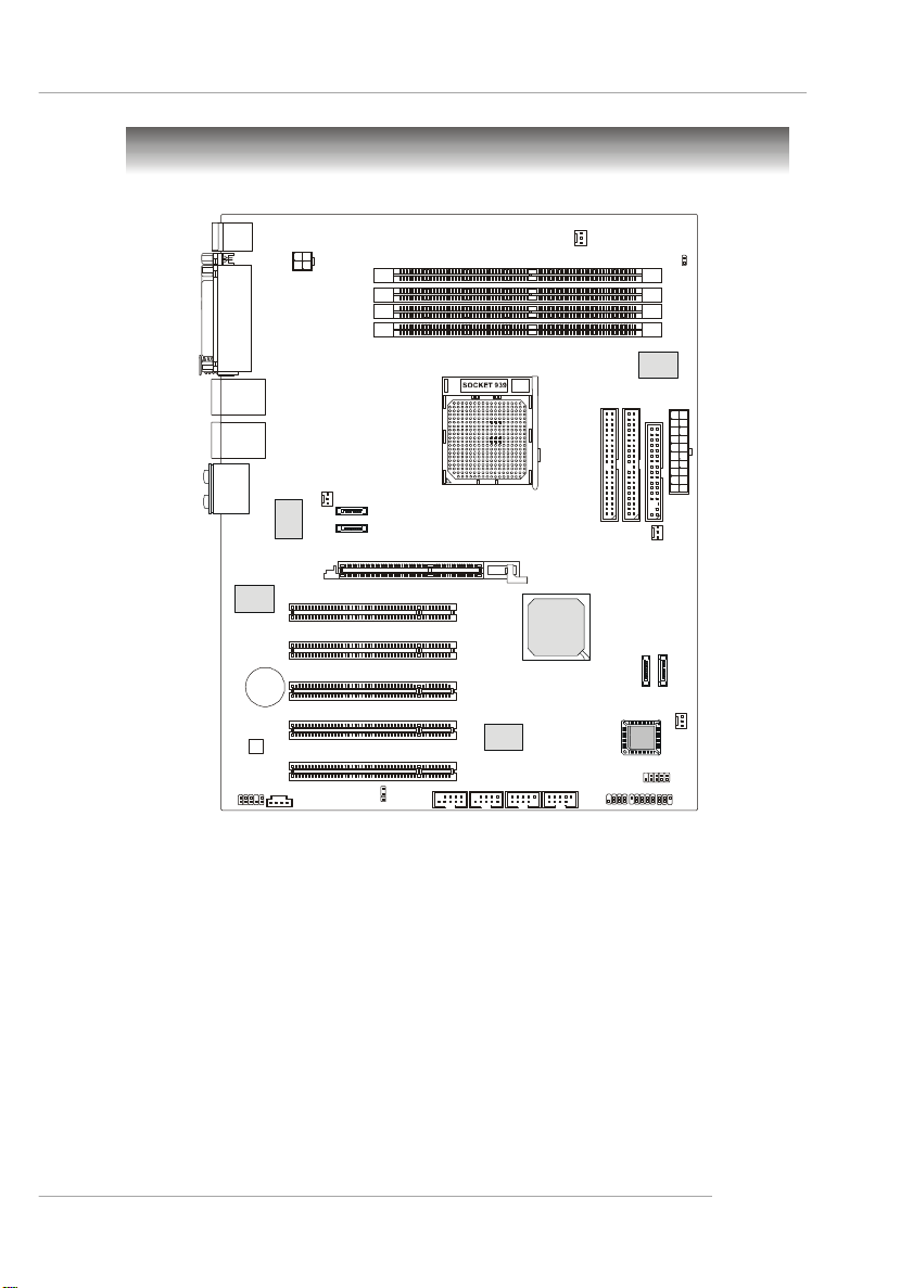
IDE 1IDE 2ATX1SATA2
SATA4
SATA3
PCI Slot 1
PCI Slot 4
PCI Slot 5
J1394_2
J1394_1
CPUFAN1NBFAN1
JFP1
JDB1
JIR1
JFP2
BATT
FDD 1
Winbond
W83627HF
Top : mouse
SFAN2
NVIDIA
nFORCE3
Bottom: keyboard
Top : Parallel Port
Bottom:
COM A
1394 Port
SPDIF
T: LAN jack
B: USB ports
T: LAN jack
B: USB ports
T:
Line-In
M:
Line-Out
B:
Mic
T:RS-Out
M:CS-Out
B:SPDIFOut
RTL8110S-32
Mainboard Layout
JPW1
DIMM4
DIMM3
DIMM2
DIMM1
88E1 111-RCJ
AGP1
PCI Slot2
Getting Started
JCI1
Ultra
+
PCI Slot3
VIA
Codec
JAUD1
JCD1
JBAT1
VT6306
JUSB2
JUSB1
SATA1
SFAN1
BIOS
K8N Neo2 Platinum (MS-7025 v1.X) AT X Mainboard
E-1-7
Page 13

Hardware Setup
Chapter 2. Hardware Setup
Hardware Setup
This chapter tells you how to install the CPU, memory modules,
and expansion cards, as well as how to setup the jumpers on the
mainboard. Also, it provides the instructions on connecting the peripheral devices, such as the mouse, keyboard, etc.
While doing the installation, be careful in holding the components and follow the installation procedures.
E-2-1
Page 14
MS-7025 ATX Mainboard
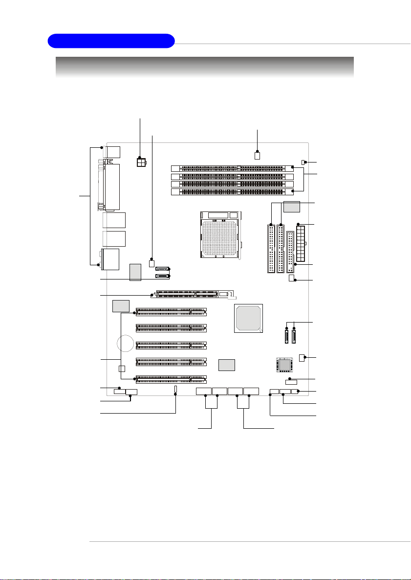
Back Panel
I/O, p.2-12
SATA3, SATA4,
AGP Slot, p.2-25
PCI Slots 1~5,
p.2-18
p.2-25
JAUD1, p.2-20
JCD1, p.2-18
JBAT1, p.2-24
J1394_1, J1394_2, p.2-20
Quick Components Guide
JPW1, p.2-10
CPUFAN1, p.2-16
BATT
+
SFAN2, p.2-16
JUSB1, JUSB2, p.2-19
JCI1, p.2-17
DDR DIMMs,
p.2-7
IDE1/2, p.2-17
ATX1, p.2-10
FDD1, p.2-16
NB_FAN1,
p.2-16
SATA2, SATA1,
p.2-18
SFAN1, p.2-16
JDB1, p.2-21
JIR1, p.2-21
JFP1, p.2-19
JFP2, p.2-19
E-2-2
Page 15
Hardware Setup
Central Processing Unit: CPU
The mainboard supports AMD® Athlon64 processor. The mainboard uses a CPU socket
called Socket-939 for easy CPU installation. When you are installing the CPU, make
sure the CPU has a heat sink and a cooling fan attached on the top to
prevent overheating. If you do not have the heat sink and cooling fan, contact your
dealer to purchase and install them before turning on the computer.
For the latest information about CPU, please visit http://www.msi.com.tw/program/
products/mainboard/mbd/pro_mbd_cpu_support.php.
MSI Reminds You...
Overheating
Overheating will seriously damage the CPU and system, always make
sure the cooling fan can work properly to protect the CPU from
overheating.
Replacing the CPU
While replacing the CPU, always turn off the ATX power supply or
unplug the power supply’s power cord from grounded outlet first to
ensure the safety of CPU.
Overclocking
This motherboard is designed to support overclocking. However, please
make sure your components are able to tolerate such abnormal setting,
while doing overclocking. Any attempt to operate beyond product specifications is not recommended. We do not guarantee the damages
or risks caused by inadequate operation or beyond product
specifications.
E-2-3
Page 16
MS-7025 ATX Mainboard
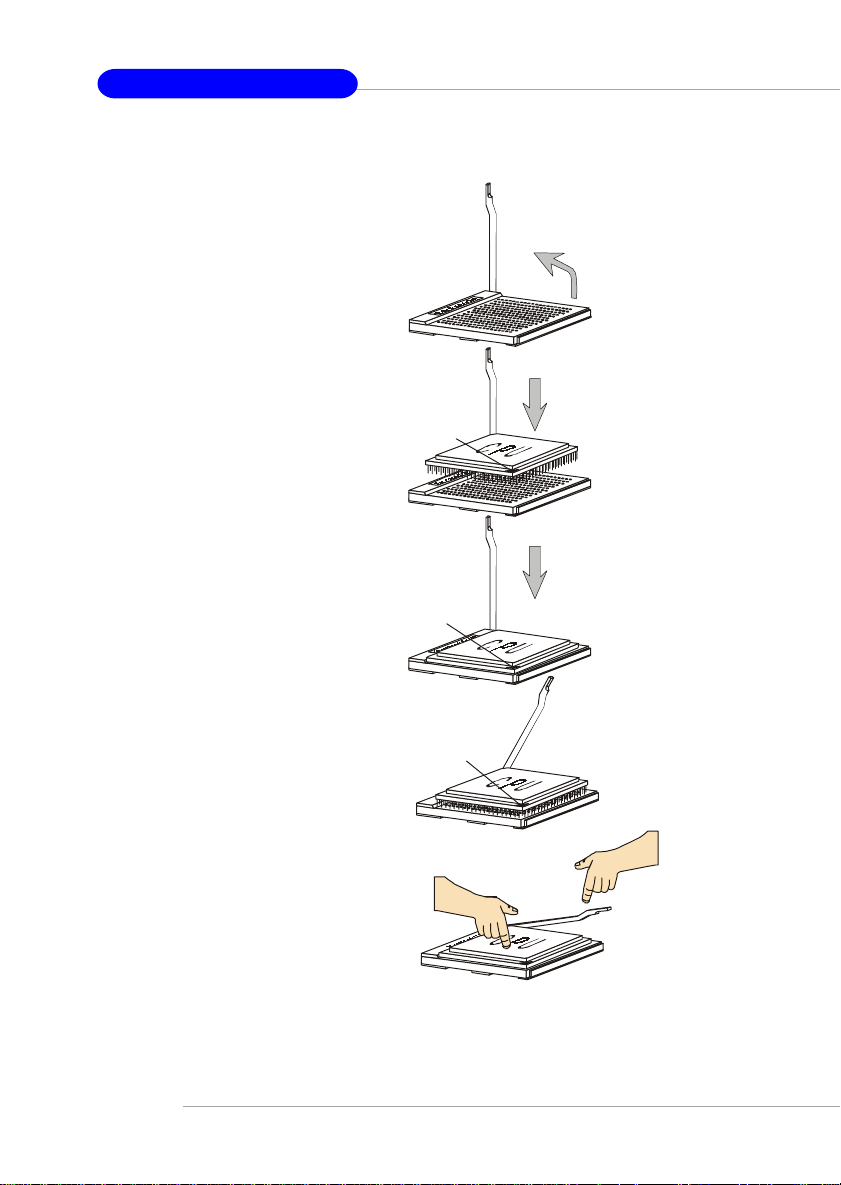
CPU Installation Procedures for Socket 939
1. Please turn off the power and
unplug the power cord before
installing the CPU.
2. Pull the lever sideways away
from the socket. Make sure to
raise the lever up to a 90-degree angle.
3. Look for the gold arrow. The gold
arrow should point towards the
lever pivot. The CPU can only fit
in the correct orientation.
4. If the CPU is correctly installed,
the pins should be completely
embedded into the socket and
can not be seen. Please note
that any violation of the correct
installation procedures may
cause permanent damages to
your mainboard.
Sliding
Plate
Gold arrow
Gold arrow
Gold arrow
Gold arrow
Open Lever
90 degree
Correct CPU placement
O
Incorrect CPU placement
X
5. Press the CPU down firmly into
the socket and close the lever.
As the CPU is likely to move while
the lever is being closed, always close the lever with your
fingers pressing tightly on top of
the CPU to make sure the CPU is
properly and completely embedded into the socket.
E-2-4
Press down
the CPU
Close
Lever
Page 17
Hardware Setup
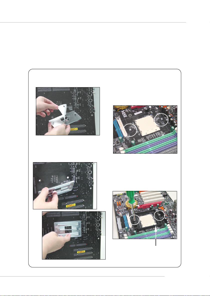
Installing AMD Athlon64 CPU Cooler Set
When you are installing the CPU, make sure the CPU has a heat sink and a
cooling fan attached on the top to prevent overheating. If you do not have the
heat sink and cooling fan, contact your dealer to purchase and install them before
turning on the computer.
1. Detach the shield of the backplate’s
paster.
2. Turn over the mainboard, and install
the backplate to the proper position.
3. Turn over the mainboard again, and
place the mainboard on the flat
surface.
Locate the two screw holes of the
mainboard.
4. Align the retention mechanism and
the backplate.
Fix the retention mechanism and the
backplate with two screws.
retention mechanism
E-2-5
Page 18
MS-7025 ATX Mainboard
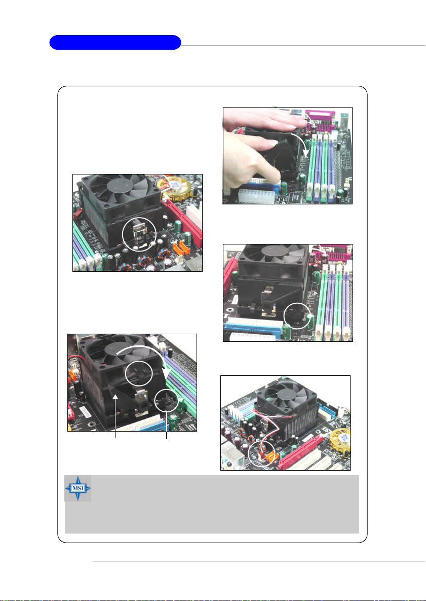
5. Position the cooling set onto the retention mechanism.
Hook one end of the clip to hook first,
and then press down the other end
of the clip to fasten the cooling set
on the top of the retention mechanism.
6. Locate the Fix Lever, Saftey Hook
and the Fixed Bolt.
Lift up the intensive fixed lever.
Safety Hook
7. Fastened down the lever.
8. Make sure the safety hook completely
clasps the fixed bolt of the retention
mechanism.
9. Attach the CPU Fan cable to the CPU
fan connector on the mainboard.
E-2-6
Fixed Lever
MSI Reminds You...
While disconnecting the Safety Hook from the fixed bolt, it is necessary to keep an eye on your fingers, because once the Safety Hook is
disconnected from the fixed bolt, the fixed lever will spring back instantly.
Fixed Bolt
Page 19
Hardware Setup
Memory
The mainboard provides 4 slots for 184-pin DDR SDRAM DIMM (Double In-Line Memory
Module) modules and supports the memory size up to 4GB. You can install DDR266/
333/400/433/466/500/533 modules on the DDR DIMM slots (DDR 1~4).
For the updated supporting memory modules, please visit http://www.msi.com.tw/
program/products/mainboard/mbd/pro_mbd_trp_list.php.
DIMM1~4
(from bottom to top)
Introduction to DDR SDRAM
DDR (Double Data Rate) SDRAM is similar to conventional SDRAM, but doubles the
rate by transferring data twice per cycle. It uses 2.5 volts as opposed to 3.3 volts
used in SDR SDRAM, and requires 184-pin DIMM modules rather than 168-pin DIMM
modules used by SDR SDRAM. High memory bandwidth makes DDR an ideal solution
for high performance PC, workstations and servers.
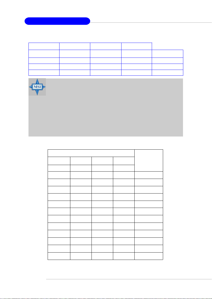
DIMM Module Combination
Install at least one DIMM module on the slots. Each DIMM slot supports up to a maximum
size of 1GB. Users can install either single- or double-sided modules to meet their
own needs. Please note that each DIMM can work respectively for single-
channel DDR, but there are some rules while using dual-channel DDR (Please
refer to the suggested DDR population table below). Users may install memory modules
of different type and density on different-channel DDR DIMMs. However, the same
type and density memory modules are necessary while using dual-channel DDR,
or instability may happen. Please refer to the following table for detailed dual-channel
DDR. Other combination not listed below will function as single-channel DDR.
E-2-7
Page 20
MS-7025 ATX Mainboard
GREEN
DIMM1 (Ch A) DIMM2 (Ch B) DIMM3 (Ch A) DIMM4 (Ch B) System Density
128MB~1GB 128MB~1GB 256MB~2GB
128MB~1GB 128MB~1GB 128MB~1GB 128MB~1GB 512MB~4GB
MSI Reminds You...
- Dual-channel DDR works ONLY in the 3 combinations listed in
- Please select the identical memory modules to install on the dual
- Always insert the memory modules into the GREEN slots first, and
- This mainboard DO NOT support the memory module installed
PURPLE
the table shown in the previous page.
channel, and DO NOT install three memory modules on three
DIMMs, or it may cause some unkonwn failure.
it is strongly recommended not to insert the memory modules into
the PURPLE slots while the GREEN slots are left empty.
with more than 18 pieces of IC (integrated circuit).
GREEN
128MB~1GB 128MB~1GB 256MB~2GB
PURPLE
Recommended Memory Combination List
DIMM Slots
Green
DIMM1
S
D
Purple
DIMM2 DIMM3 DIMM4
--
-
-
-
S-
D-
S
S
--SS
DD
--
S
D
S
D
Green
Purple
-
S
-
D-
-
-
-
S-
D-
-
-
-DD
S
D
S
D
Max Speed
DDR 400
DDR 400
DDR 400
DDR 400
DDR 400
DDR 333
DDR 400
DDR 400
DDR 400
DDR 400
DDR 400
DDR 333
E-2-8
S: Single Side D: Double Side
Page 21
Hardware Setup
MSI Reminds You...
1. The maximum memory speed decreases when the following two
Memory Combination is selected (you can also refer to the Recommended Memory Combination list shown in the previous page:
- Each channel is installed with two double-sided memory mod-
ules
- Both DIMM1 and DIMM3 slots are installed with double-sided
memory module.
2. Due to the South Bridge resource deployment, the system density will only be detected up to 3+GB (not full 4GB) when each
DIMM is installed with an 1GB memory module.
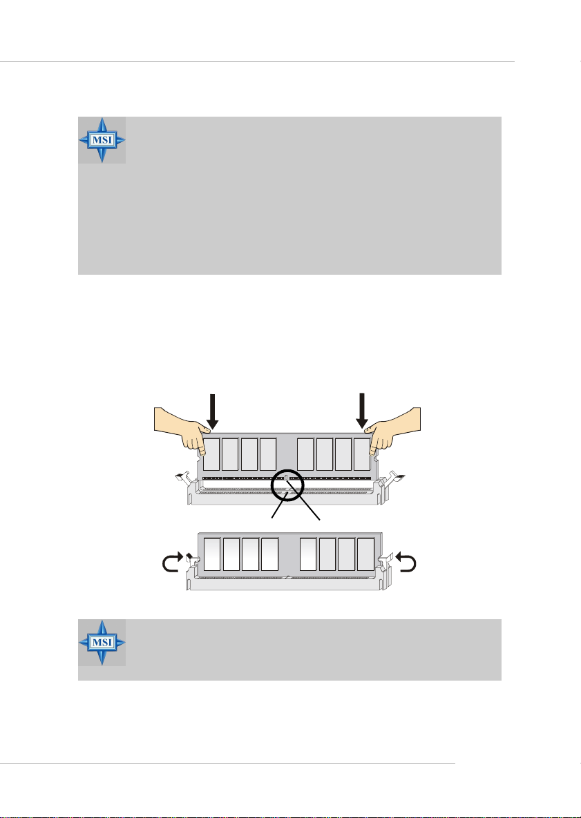
Installing DDR Modules
1. The DDR DIMM has only one notch on the center of module. The module will only
fit in the right orientation.
2. Insert the DIMM memory module vertically into the DIMM slot. Then push it in until
the golden finger on the memory module is deeply inserted in the socket.
3. The plastic clip at each side of the DIMM slot will automatically close.
Volt
MSI Reminds You...
You can barely see the golden finger if the module is properly inserted in the socket.
Notch
E-2-9
Page 22
MS-7025 ATX Mainboard
Power Supply
The mainboard supports ATX power supply for the power system. Before inserting
the power supply connector, always make sure that all components are installed
properly to ensure that no damage will be caused.
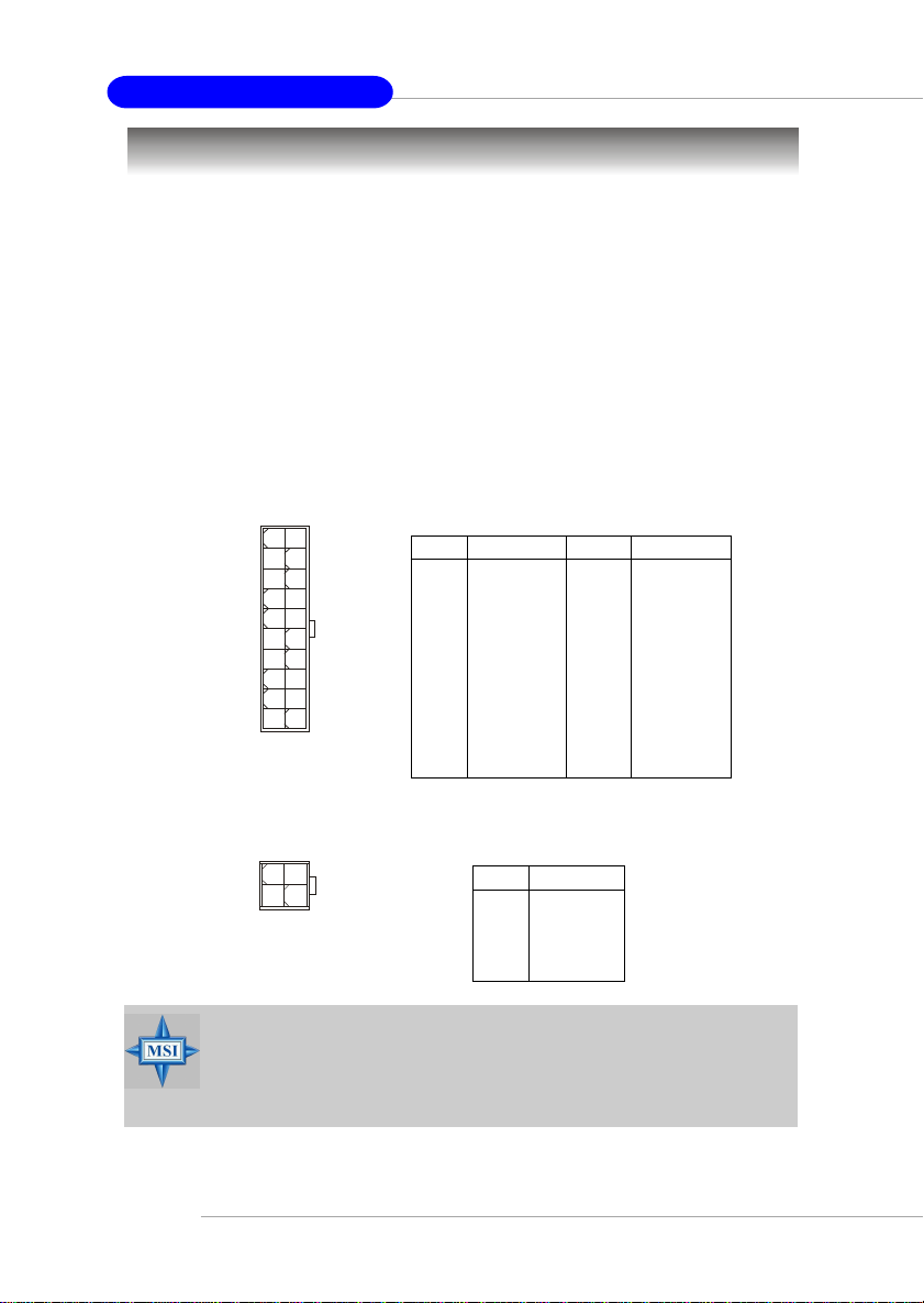
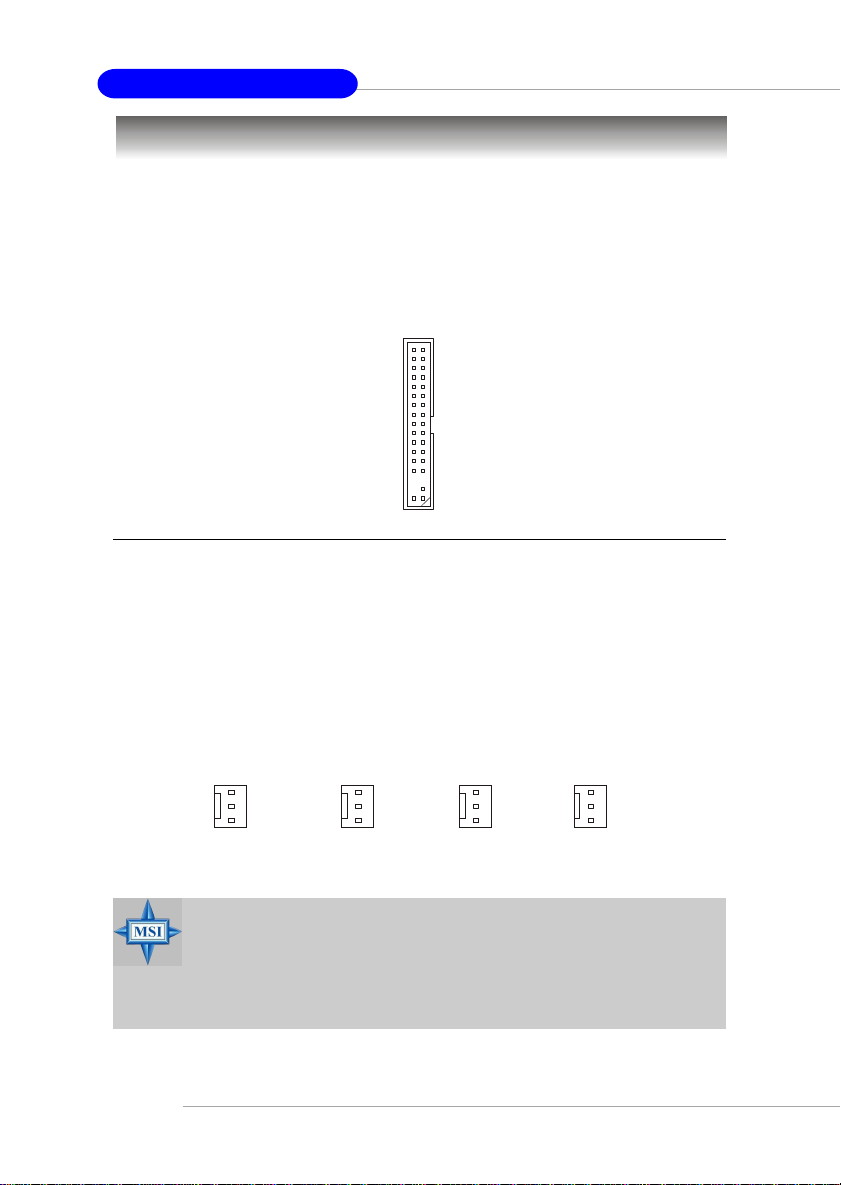
A TX 20-Pin Power Connector: ATX1
This connector allows you to connect to an ATX power supply. To connect to the ATX
power supply, make sure the plug of the power supply is inserted in the proper
orientation and the pins are aligned. Then push down the power supply firmly into the
connector.
ATX 12V Power Connector: JPW1
This 12V power connector is used to provide power to the CPU.
10
1
20
11
ATX1
13
42
JPW1
ATX1 Pin Definition
PIN SIGNAL
1 3.3V
2 3.3V
3 GND
45V
5 GND
65V
7 GND
8 PW_OK
9 5V_SB
10 12V
JPW1 Pin Definition
PIN SIGNAL
1 GND
2 GND
3 12V
4 12V
PIN SIGNAL
11 3.3V
12 -12V
13 GND
14 PS_ON
15 GND
16 GND
17 GND
18 -5V
19 5V
20 5V
MSI Reminds You...
1. These two connectors connect to the ATX power supply and have to
work together to ensure stable operation of the mainboard.
2. Power supply of 300 (and up) watt is highly recommended for system
stability.
E-2-10
Page 23
Hardware Setup
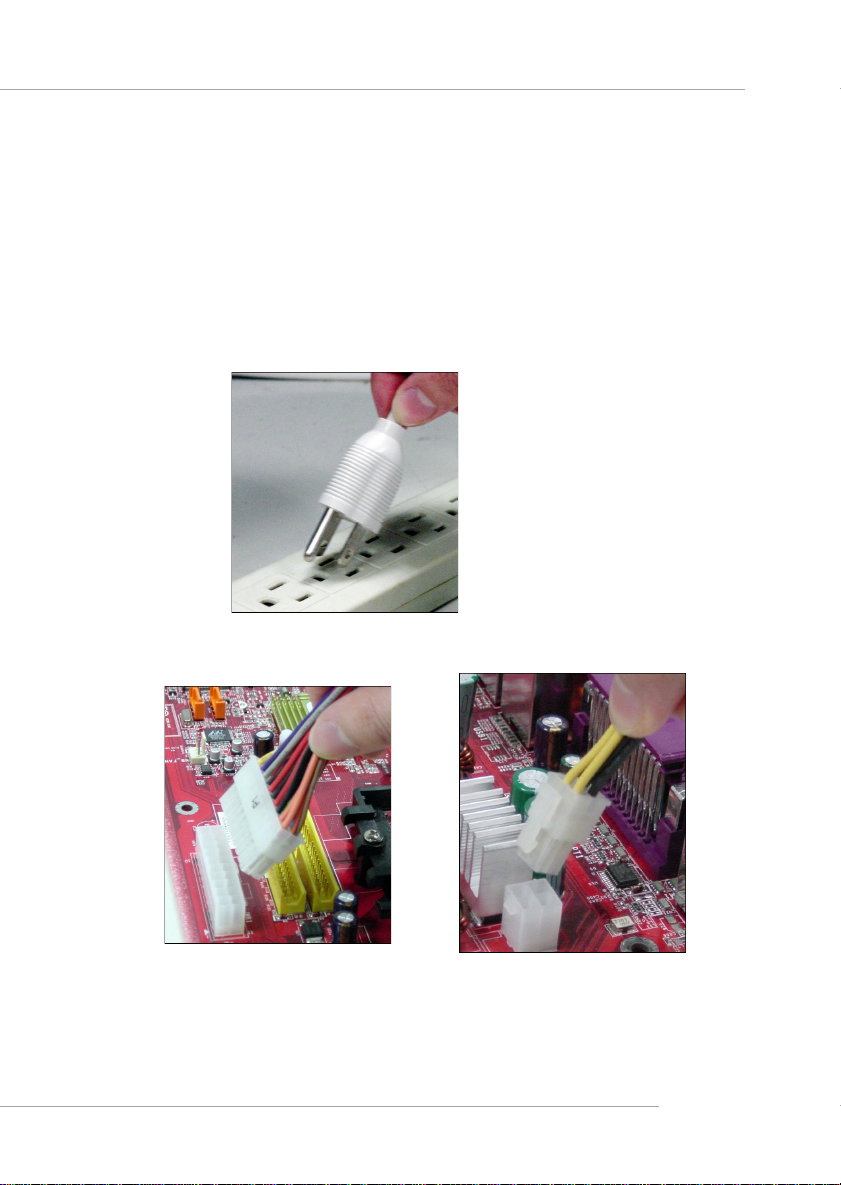
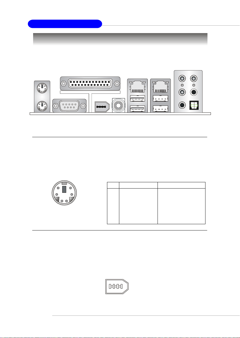
Important Notification about Power Issue
NForce chipset is very sensitive to ESD (Electrostatic Discharge), therefore this
issue mostly happens while the users intensively swap memory modules under S5
(power-off) states, and the power code is plugged while installing modules. Due to
several pins are very sensitive to ESD, so this kind of memory-replacement actions
might cause chipset system unable to boot. Please follow the following solution to
avoid this situation.
Unplug the AC power cable (shown in figure 1) or unplug the ATX1 & JPW1 power
connectors (shown in figure 2 & figure 3) before the 1st installation or during system upgrade procedure.
Unplug the ATX1 power connector
Figure 2:
Unplug the AC power cable
Figure 1:
Figure 3:
Unplug the JPW1 power connector
E-2-11
Page 24
MS-7025 ATX Mainboard
Back Panel
The back panel provides the following connectors:
Mouse
Parallel
LAN
LAN
L-In
RS-Out
Keyboard
COM A
1394 Port
(Optional)
SPDIF
Out
(Coaxial)
USB Ports
L-Out
Mic
CS-Out
SPDIF Out
(Optical)
Mouse Connector (Green) / Keyboard Connector (Purple)
The mainboard provides a standard PS/2® mouse/keyboard mini DIN connector for
attaching a PS/2® mouse/keyboard. You can plug a PS/2® mouse/keyboard directly
into this connector. The connector location and pin assignments are as follows:
Pin Definition
6
4
2
PS/2 Mouse / Keyboard
(6-pin Female)
5
3
1
PIN SIGNAL DESCRIPTION
1 Mouse/Keyboard Data Mouse/Keyboard data
2 NC No connection
3 GND Ground
4 VCC +5V
5 Mouse/Keyboard Clock Mouse/Keyboard clock
6 NC No connection
IEEE1394 Port (Optional)
The back panel provides one standard IEEE 1394 port. The standard IEEE1394 port
connects to IEEE1394 devices without external power. The IEEE1394 high-speed
serial bus complements USB by providing enhanced PC connectivity for a wide range
of devices, including consumer electronics audio/video (A/V) appliances, storage
peripherals, other PCs, and portable devices.
E-2-12
IEEE1394 Port
Page 25
Hardware Setup
Serial Port Connector
The mainboard offers one 9-pin male DIN connector as the serial port. The port is a
16550A high speed communication port that sends/receives 16 bytes FIFOs. You
can attach a serial mouse or other serial devices directly to the connector.
Pin Definition
1 2 3 4 5
6 7 8 9
9-Pin Male DIN Connector
PIN SIGNAL DESCRIPTION
1 DCD Data Carry Detect
2 SIN Serial In or Receive Data
3 SOUT Serial Out or Transmit Data
4 DTR Data T erminal Ready)
5 GND Ground
6 DSR Data Set Ready
7 RTS Request To Send
8 CTS Clear To Send
9 RI Ring Indicate
USB Connectors
The mainboard provides two OHCI (Open Host Controller Interface) Universal Serial
Bus roots for attaching USB devices such as keyboard, mouse or other USB-compatible devices. You can plug the USB device directly into the connector.
1 2 3 4
5 6 7 8
USB Ports
USB Port Description
PIN SIGNAL DESCRIPTION
1 VCC +5V
2 -Data 0 Negative Data Channel 0
3 +Data0 Positive Data Channel 0
4 GND Ground
5 VCC +5V
6 -Data 1 Negative Data Channel 1
7 +Data 1 Positive Data Channel 1
8 GND Ground
E-2-13
Page 26
MS-7025 ATX Mainboard
LAN (RJ-45) Jack
The mainboard provides 2 standard RJ-45 jacks for connection to single Local Area
Network (LAN). This Giga-bit LAN enables data to be transferred at 1000, 100 or
10Mbps. You can connect a network cable to either LAN jack.
Giga-bit LAN Pin Definition
PIN SIGNAL DESCRIPTION
1 D0P Differential Pair 0+
2 D0N Differential Pair 03 D1P Differential Pair 1+
RJ-45 LAN Jack
4 D2P Differential Pair 2+
5 D2N Differential Pair 26 D1N Differential Pair 17 D3P Differential Pair 3+
8 D3N Differential Pair 3-
Audio Port Connectors
The left 3 audio jacks are for 2-channel mode for stereo speaker output: Line Out is
a connector for Speakers or Headphones. Line In is used for external CD player,
Tape player, or other audio devices. Mic is a connector for microphones.
However, there is an advanced audio application provided by Realtek ALC850 to
offer support for 7.1-channel audio operation and can turn rear audio connectors
from 2-channel to 4-/5.1-/7.1 channel audio.
E-2-14
Line In
Line Out
MIC
S/PDIF Out-Coaxial
Rear Speaker Out
(in 7.1CH / 6CH)
Center/Subwoofer
Speaker Out
( in 7.1CH / 6CH)
S/PDIF Out-Optical
(in 7.1CH / 6CH)
Page 27
Hardware Setup
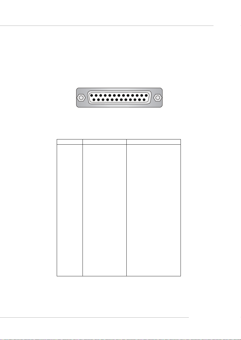
Parallel Port Connector: LPT1
The mainboard provides a 25-pin female centronic connector as LPT. A parallel port
is a standard printer port that supports Enhanced Parallel Port (EPP) and Extended
Capabilities Parallel Port (ECP) mode.
13 1
25
14
Pin Definition
PIN SIGNAL DESCRIPTION
1 STROBE Strobe
2 DAT A0 Data0
3 DAT A1 Data1
4 DAT A2 Data2
5 DAT A3 Data3
6 DAT A4 Data4
7 DAT A5 Data5
8 DAT A6 Data6
9 DAT A7 Data7
10 ACK# Acknowledge
11 BUSY Busy
12 PE Paper End
13 SELECT Select
14 AUTO FEED# Automatic Feed
15 ERR# Error
16 INIT# Initialize Printer
17 SLIN# Select In
18 GND Ground
19 GND Ground
20 GND Ground
21 GND Ground
22 GND Ground
23 GND Ground
24 GND Ground
25 GND Ground
E-2-15
Page 28
MS-7025 ATX Mainboard
Connectors
The mainboard provides connectors to connect to FDD, IDE HDD, case, LAN, USB
Ports, IR module and CPU/System FAN.
Floppy Disk Drive Connector: FDD1
The mainboard provides a standard floppy disk drive connector that supports 360K,
720K, 1.2M, 1.44M and 2.88M floppy disk types.
FDD1
Fan Power Connectors: CPUFAN1 / SFAN1 / SF AN2 / NBF A N1
The CPUFAN1 (processor fan), SFAN1 (system fan 1), SFAN2 (system fan 2) and
NBFAN1 (NorthBridge Chipset fan) support system cooling fan with +12V. It supports
three-pin head connector. When connecting the wire to the connectors, always take
note that the red wire is the positive and should be connected to the +12V, the black
wire is Ground and should be connected to GND. If the mainboard has a System
Hardware Monitor chipset on-board, you must use a specially designed fan with
speed sensor to take advantage of the CPU fan control.
E-2-16
GND
+12V
SENSOR
CPUFAN1
SFAN1
GND
+12V
NC
SFAN2
GND
+12V
NC
GND
+12V
Sensor
NBFAN1
MSI Reminds You...
1. Always consult the vendors for proper CPU cooling fan.
2. CPUFAN1 supports fan control. You can install Core Center utility that will automatically control the CPU fan speed according to
the actual CPU temperature.
3. Please refer to the recommended CPU fans at AMD® official
website.
Page 29

Hardware Setup
Hard Disk Connectors: IDE1 / IDE2
The mainboard has a 32-bit Enhanced PCI IDE and Ultra DMA 33/66/100/133 controller
that provides PIO mode 0~4, Bus Master, and Ultra DMA 33/66/100/133 function. You
can connect up to four hard disk drives, CD-ROM, or other devices.
IDE1IDE2
IDE1 (Primary IDE Connector)
The first hard drive should always be connected to IDE1. IDE1 can connect a Master
and a Slave drive. You must configure second hard drive to Slave mode by setting the
jumper accordingly.
IDE2 (Secondary IDE Connector)
IDE2 can also connect a Master and a Slave drive.
MSI Reminds You...
If you install two hard disks on cable, you must configure the second
drive to Slave mode by setting its jumper. Refer to the hard disk
documentation supplied by hard disk vendors for jumper setting
instructions.
Chassis Intrusion Switch Connector: JCI1
This connector is connected to a 2-pin chassis switch. If the chassis is opened, the switch will be short. The system will record this
status and show a warning message on the screen. To clear the
warning, you must enter the BIOS utility and clear the record.
GND
CINTRU
2
1
JCI1
E-2-17
Page 30

MS-7025 ATX Mainboard
Serial ATA/Serial ATA RAID Connectors controlled by
nForce3 Ultra: SA TA1 / SAT A2 / SATA3 / SAT A4
The Southbridge of this mainboard is nForce3 Ultra which supports four serial
ATA connectors SATA1~SATA4.
SATA1~SATA4 are dual high-speed Serial ATA interface ports. Each supports
1st generation serial ATA data rates of 150 MB/s. Both connectors are fully compliant
with Serial ATA 1.0 specifications. Each Serial ATA connector can connect to 1 hard
disk device. Please refer to the nVidia RAID Introduction for detail software installation procedure.
SATA3
SATA4
71
SATA27SATA1
1
Serial ATA cable
SAT A1~ SA TA4 Pin Definition
PIN SIGNAL PIN SIGNAL
1 GND 2 TXP
3 TXN 4 GND
5 RXN 6 RXP
7 GND
Connect to serial ATA ports
MSI Reminds You...
Please do not fold the serial ATA cable in a 90-degree angle, which will
cause the loss of data during the transmission.
CD-In Connector: JCD1
The connector is for CD-ROM audio connector.
E-2-18
Take out the dust cover and
connect to the hard disk
devices
L
JCD1
GND
R
Page 31

Hardware Setup
Front Panel Connectors: JFP1 / JFP2
The mainboard provides two front panel connectors for electrical connection
to the front panel switches and LEDs. JFP1 is compliant with Intel® Front Panel I/O
Connectivity Design Guide.
JFP1
Reset
HDD
Switch
LED
9
10
Power
Switch
Power
LED
1
2
PIN SIGNAL DESCRIPTION
1 HD_LED_P Hard disk LED pull-up
2 FP PWR/SLP MSG LED pull-up
3 HD_LED_N Hard disk active LED
4 FP PWR/SLP MSG LED pull-up
5 RST_SW_N Reset Switch low reference pull-down to GND
6 PWR_SW_P Power Switch high reference pull-up
7 RST_SW_P Reset Switch high reference pull-up
8 PWR_SW_N Power Switch low reference pull-down to GND
9 RSVD_DNU Reserved. Do not use.
JFP1 Pin Definition
JFP2 Pin Definition
PIN SIGNAL PIN SIGNAL
1 GND 2 SPK3 SLED 4 BUZ+
5 PLED 6 BUZ7 NC 8 SPK+
JFP2
2
1
Speaker
Power
LED
8
7
Front USB Connectors: JUSB1 / JUSB2
The mainboard provides two standard USB 2.0 pin headers JUSB1 & JUSB2 .
USB 2.0 technology increases data transfer rate up to a maximum throughput of
480Mbps, which is 40 times faster than USB 1.1, and is ideal for connecting highspeed USB interface peripherals such as USB HDD, digital cameras, MP3 players,
printers, modems and the like.
JUSB1 & JUSB2 Pin Definition
PIN SIGNAL PIN SIGNAL
2 10
1
9
JUSB1, JUSB2
(USB 2.0)
Connected to JUSB1 or JUSB2
(the USB pinheader in YELLOW color)
1 VCC 2 VCC
3 USB0- 4 USB15 USB0+ 6 USB1+
7 GND 8 GND
9 Key (no pin) 1 0 USBOC
USB 2.0 Bracket
(Optional)
E-2-19
Page 32

MS-7025 ATX Mainboard
Front Panel Audio Connector: JAUD1
The JAUD1 front panel audio connector allows you to connect to the front
panel audio and is compliant with Intel® Front Panel I/O Connectivity Design Guide.
Pin Definition
PIN SIGNAL DESCRIPTION
1 AUD_MIC Front panel microphone input signal
2 AUD_GND Ground used by analog audio circuits
3 AUD_MIC_BIAS Microphone power
10
4 AUD_VCC Filtered +5V used by analog audio circuits
9
5 AUD_FPOUT_R Right channel audio signal to front panel
6 AUD_RET_R Right channel audio signal return from front panel
7 HP_ON Reserved for future use to control headphone amplifier
8 KEY No pin
9 AUD_FPOUT_L Left channel audio signal to front panel
10 AUD_RET_L Left channel audio signal return from front panel
2
1
JAUD1
MSI Reminds You...
If you don’t want to connect to the front audio header,
pins 5 & 6, 9 & 10 have to be jumpered in order to have
6
10
signal output directed to the rear audio ports. Otherwise,
the Line-Out connector on the back panel will not
5
9
function.
IEEE 1394 Connectors: J1394_1 / J1394_2 (Optional)
The mainboard provides two 1394 pin headers that allow you to connect IEEE
1394 ports via an external IEEE1394 bracket (optional).
2
1
10
9
J1394_1, J1394_2
Foolproof Design
(the 1394 pinheader in GREEN color)
E-2-20
Pin Definition
PIN SIGNAL PIN SIGNAL
1TPA+ 2 TPA3 Ground 4 Ground
5 TPB+ 6 TPB7 Cable power 8 Cable power
9 Key (no pin) 10 Ground
IEEE1394 Bracket
Page 33

Hardware Setup
IrDA Infrared Module Header: JIR1
The connector allows you to connect to IrDA Infrared module. You must configure the setting through the BIOS setup to use the IR function. JIR1 is compliant with
Intel® Front Panel I/O Connectivity Design Guide.
JIR1 Pin Definition
6 5
21
JIR1
Pin Signal Pin Signal
1NC 2 NC
3 VCC5 4 GND
5 IRTX 6 IRRX
D-Bracket™ 2 Connector: JDB1 (Optional)
The mainboard comes with a JDB1 connector for you to connect to D-Bracket™ 2. DBracket™ 2 is a USB Bracket that supports both USB1.1 & 2.0 spec. It integrates four
LEDs and allows users to identify system problem through 16 various combinations
of LED signals.
Pin Definition
Pin Signal
1 DBG1 (high for green color)
2
1
Connected to JDB1
JDB1
10
9
2 DBR1 (high for red color)
3 DBG2 (high for green color)
4 DBR2 (high for red color)
5 DBG3 (high for green color)
6 DBR3 (high for red color)
7 DBG4 (high for green color)
8 DBR4 (high for red color)
9 Key
10 NC
D-Bracket™ 2
(Optional)
Connected to JUSB1 or JUSB2
(the USB pinheader in YELLOW color)
LEDs
E-2-21
Page 34

MS-7025 ATX Mainboard
D-Bracket™ 2 is an external USB bracket integrating four Diagnostic LEDs, which
use graphic signal display to help users understand their system. The LEDs provide
up to 16 combinations of signals to debug the system. The 4 LEDs can debug all
problems that fail the system, such as VGA, RAM or other failures. This special
feature is very useful for the overclocking users. These users can use the feature to
detect if there are any problems or failures.
D-Bracket™ 2 supports both USB 1.1 & 2.0 specification.
D-Bracket™ 2
Red
D-Bracket™ 2
1 2
3 4
1 2
3 4
Green
Description
System Power ON
The D-LED will hang here if the processor is damaged or
not installed properly.
Early Chipset Initialization
Memory Detection Test
Testing onboard memory size. The D-LED will hang if the
memory module is damaged or not installed properly.
Decompressing BIOS image to RAM for fast booting.
Initializing Keyboard Controller.
E-2-22
Testing VGA BIOS
This will start writing VGA sign-on message to the screen.
Page 35

Hardware Setup
D-Bracket™ 2
1 2
3 4
Description
Processor Initialization
This will show information regarding the processor (like
brand name, system bus, etc...)
T esting RTC (Real T ime Clock)
Initializing Video Interface
This will start detecting CPU clock, checking type of video
onboard. Then, detect and initialize the video adapter.
BIOS Sign On
This will start showing information about logo, processor brand name, etc...
Testing Base and Extended Memory
Testing base memory from 240K to 640K and extended
memory above 1MB using various patterns.
Assign Resources to all ISA.
Initializing Hard Drive Controller
This will initialize IDE drive and controller.
Initializing Floppy Drive Controller
This will initialize Floppy Drive and controller.
Boot Attempt
This will set low stack and boot via INT 19h.
Operating System Booting
E-2-23
Page 36

MS-7025 ATX Mainboard
Jumpers
The motherboard provides the following jumpers for you to set the computer’s
function. This section will explain how to change your motherboard’s function through
the use of jumpers.
Clear CMOS Jumper: JBA T1
There is a CMOS RAM on board that has a power supply from external battery
to keep the system configuration data. With the CMOS RAM, the system can automatically boot OS every time it is turned on. If you want to clear the system
configuration, use the JBAT1 (Clear CMOS Jumper ) to clear data. Follow the instructions below to clear the data:
1
JBAT1
MSI Reminds You...
You can clear CMOS by shorting 2-3 pin while the system is off.
Then return to 1-2 pin position. Avoid clearing the CMOS while the
system is on; it will damage the mainboard.
Keep Data
3
Clear Data
1
E-2-24
Page 37
Hardware Setup
Slots
The mainboard provides one AGP slot and five 32-bit PCI bus slots.
AGP (Accelerated Graphics Port) Slot
The AGP slot allows you to insert the AGP graphics card. AGP is an interface
specification designed for the throughput demands of 3D graphics. It introduces a
66MHz, 32-bit channel for the graphics controller to directly access main memory.
The slot supports 8x/4x AGP card.
AGP Slot
PCI (Peripheral Component Interconnect) Slots
The PCI slots allow you to insert the expansion cards to meet your needs.
When adding or removing expansion cards, make sure that you unplug the power
supply first. Meanwhile, read the documentation for the expansion card to make any
necessary hardware or software settings for the expansion card, such as jumpers,
switches or BIOS configuration.
The orange PCI slot (PCI5) also works as a communication slot, which allows
you to insert the MSI communication card.
PCI Slots
PCI Interrupt Request Routing
The IRQ, acronym of interrupt request line and pronounced I-R-Q, are hardware lines over which devices can send interrupt signals to the microprocessor. The
PCI IRQ pins are typically connected to the PCI bus INT A# ~ INT D# pins as follows:
Order 1 Order 2 Order 3 Order 4
PCI Slot 1 INT A# INT B# INT C# INT D#
PCI Slot 2 INT B# INT C# INT D# INT A#
PCI Slot 3 INT C# INT D # INT A# INT B#
PCI Slot 4 INT D# INT A# INT B# INT C#
PCI Slot 5 INT B# INT C# INT D# INT A#
E-2-25
Page 38

BIOS Setup
Chapter 3. BIOS Setup
BIOS Setup
This chapter provides information on the BIOS Setup program and allows
you to configure the system for optimum use.
You may need to run the Setup program when:
² An error message appears on the screen during the system
booting up, and requests you to run SETUP.
² You want to change the default settings for customized
features.
MSI Reminds You...
1. The items under each BIOS category described in this chapter are
under continuous update for better system performance.
Therefore, the description may be slightly different from the latest
BIOS and should be held for reference only.
2. While booting up, the BIOS version is shown in the 1st line appearing after the memory counting. It is usually in the format:
example: W7025NMS V1.0B32 061704
where:
1st digit refers to BIOS maker as A=AMI(R); W=AWARD(R)
2nd - 5th digit refers to the model number.
6th digit refers to nVIDIA chipset.
7th - 8th digit refers to the customer, MS=all standard customers.
V1.0 refers to the BIOS version.
061704 refers to the date this BIOS is released.
E-3-1
Page 39

MS-7025 ATX Mainboard
Entering Setup
Power on the computer and the system will start POST (Power On Self Test) process.
When the message below appears on the screen, press <DEL> key to enter Setup.
Press DEL to enter SETUP
If the message disappears before you respond and you still wish to enter Setup,
restart the system by turning it OFF and On or pressing the RESET button. You may
also restart the system by simultaneously pressing <Ctrl>, <Alt>, and <Delete> keys.
Selecting the First Boot Device
You are allowed to select the 1st boot device without entering the BIOS setup utility
by pressing <F11>. When the same message as listed above appears on the screen,
press <F11> to trigger the boot menu.
The POST messages might pass by too quickly for you to respond in time. If so,
restart the system and press <F11> after around 2 or 3 seconds to activate the boot
menu similar to the following.
Select First Boot Devic e
Floppy : 1st Flop py
IDE-0 : IBM-DTLA -307038
CD ROM : ATAPI CD-ROM DRIVE 40X M
[Up/Dn] Selec t [RETURN] Boot [ESC] cancel
The boot menu will list all the bootable devices. Select the one you want to boot from
by using arrow keys, then press <Enter>. The system will boot from the selected
device. The selection will not make changes to the settings in the BIOS setup utility,
so next time when you power on the system, it will still use the original first boot
device to boot up.
MSI Reminds You...
The items under each BIOS category described in this chapter are
under continuous update for better system performance. Therefore,
the description may be slightly different from the latest BIOS and
should be held for reference only.
E-3-2
Page 40

BIOS Setup
Control Keys
<↑> Move to the previous item
<↓> Move to the next item
<←> Move to the item in the left hand
<→> Move to the item in the right hand
<Enter> Select the item
<Esc> Jumps to the Exit menu or returns to the main menu from a
submenu
<+/PU> Increase the numeric value or make changes
<-/PD> Decrease the numeric value or make changes
<F5> Previous Values
<F6> Load Fail-Safe Defaults
<F7> Load Optimized Defaults
<F10> Save all the CMOS changes and exit
Getting Help
After entering the Setup menu, the first menu you will see is the Main Menu.
Main Menu
The main menu lists the setup functions you can make changes to. You can use
the arrow keys ( ↑↓ ) to select the item. The on-line description of the highlighted
setup function is displayed at the bottom of the screen.
Sub-Menu
If you find a right pointer symbol (as shown in the right view) appears to the left
of certain fields that means a sub-menu can be launched from this field. A submenu contains additional options for a field
parameter. You can use arrow keys ( ↑↓ ) to
highlight the field and press <Enter> to call up
the sub-menu. Then you can use the control
keys to enter values and move from field to
field within a sub-menu. If you want to return
to the main menu, just press the <Esc >.
General Help <F1>
The BIOS setup program provides a General Help screen. You can call up this screen
from any menu by simply pressing <F1>. The Help screen lists the appropriate keys
to use and the possible selections for the highlighted item. Press <Esc> to exit the
Help screen.
E-3-3
Page 41

MS-7025 ATX Mainboard
The Main Menu
Once you enter Phoenix-Award® BIOS CMOS Setup Utility, the Main Menu will
appear on the screen. The Main Menu allows you to select from twelve setup functions and two exit choices. Use arrow keys to select among the items and press
<Enter> to accept or enter the sub-menu.
Standard CMOS Features
Use this menu for basic system configurations, such as time, date etc.
Advanced BIOS Features
Use this menu to setup the items of AWARD® special enhanced features.
Advanced Chipset Features
Use this menu to change the values in the chipset registers and optimize your system’s
performance.
Integrated Peripherals
Use this menu to specify your settings for integrated peripherals.
Power Management Setup
Use this menu to specify your settings for power management.
PNP/PCI Configurations
This entry appears if your system supports PnP/PCI.
H/W Monitor
Use this menu to specify your settings for hardware.
Cell Menu
Use this menu to specify your settings for CPU/AGP frequency/voltage control and
overclocking.
E-3-4
Page 42

BIOS Setup
Load Fail-Safe Setup Defaults
Use this menu to load factory default settings into the BIOS for stable system performance operations.
Load Optimized Defaults
Use this menu to load the BIOS values for the best system performance, but the
system stability may be affected.
Set Supervisor Password
Use this menu to set Supervisor Password.
Set User Password
Use this menu to set User Password.
Save & Exit Setup
Save changes to CMOS and exit setup.
Exit Without Saving
Abandon all changes and exit setup.
E-3-5
Page 43

MS-7025 ATX Mainboard
Cell Menu
The items in Cell Menu includes some important settings of CPU, AGP, DRAM
and overclocking functions.
MSI Reminds You...
Change these settings only if you are familiar with the chipset.
Current CPU / DDR Clock
These two items show the current clocks of CPU & DDR. Read-only.
DRAM Configuration
Press <Enter> to enter the sub-menu and the following screen appears:
Max Memclock (Mhz)
When it is set to Manual in “DDR Timing Setting by”, user can place an artificial
memory clock limit on the system. Please note that memory is prevented from
running faster than this frequency. Setting options: [100], [133], [166], [200].
1T/2T Memory Timing
This setting controls the SDRAM command rate. Selecting [Auto] allows SDRAM
signal controller to run at 1T (T=clock cycles) rate. Selecting [1T] makes SDRAM
signal controller run at 2T rate. 1T is faster than 2T. Setting options: [1T], [2T],
[Auto].
E-3-6
Page 44

BIOS Setup
CAS# Latency (Tcl)
This controls the CAS latency, which determines the timing delay (in clock
cycles) before SDRAM starts a read command after receiving it. Settings:
[Auto], [CL=2.0], [CL=2.5], [CL=3.0]. [CL=2.0] increases the system performance the most while [CL=3.0] provides the most stable performance.
RAS# to CAS# delay (Trcd)
When DRAM is refreshed, both rows and columns are addressed separately.
This setup item allows you to determine the timing of the transition from RAS
(row address strobe) to CAS (column address strobe). The less the clock
cycles, the faster the DRAM performance. Setting options: [Auto], [2 Bus Clocks],
[3 Bus Clocks], [4 Bus Clocks], [5 Bus Clocks], [6 Bus Clocks], [7 Bus Clocks].
Min RAS# active Time (Tras)
When the DDR Timing Setting by is set to [Manual], the field is adjustable.
This setting determines the time RAS takes to read from and write to a memory
cell. Setting options: [Auto], [5 Bus Clocks], [6 Bus Clocks], [7 Bus Clocks], [8
Bus Clocks], [9 Bus Clocks], [10 Bus Clocks], [11 Bus Clocks], [12 Bus Clocks],
[13 Bus Clocks], [14 Bus Clocks], [15 Bus Clocks].
Row Precharge Time (Trp)
This item controls the number of cycles for Row Address Strobe (RAS) to be
allowed to precharge. If insufficient time is allowed for the RAS to accumulate
its charge before DRAM refresh, refreshing may be incomplete and DRAM may
fail to retain data. This item applies only when synchronous DRAM is installed in
the system. Available settings: [Auto], [2 Bus Clocks], [3 Bus Clocks], [4 Bus
Clocks], [5 Bus Clocks], [6 Bus Clocks].
High Performance Mode
This field allows you to select the DDR timing setting. Setting to [Optimized] enables
Adjust DDR Memory Frequency automatically to be determined by SPD. Selecting
[Manual] allows users to configure these fields manually. Setting options: [Optimized],
[Manual].
Aggressive Timing
This item allows you to enable or disable the memory clock. When [Enabled] is selected,
the timing delay of memory will be shorten to increase the performance. Setting
options: [Enabled], [Disabled].
Dynamic Overclocking
Dynamic Overclocking Technology is the automatic overclocking function, included in
the MSITM’s newly developed CoreCell
TM
Technology. It is designed to detect the load
balance of CPU while running programs, and to adjust the best CPU frequency
automatically. When the motherboard detects CPU is running programs, it will speed
up CPU automatically to make the program run smoothly and faster. When the CPU is
temporarily suspending or staying in the low load balance, it will restore the default
settings instead. Usually the Dynamic Overclocking Technology will be powered only
when users' PC need to run huge amount of data like 3D games or the video process,
and the CPU frequency need to be boosted up to enhance the overall performance.
E-3-7
Page 45

MS-7025 ATX Mainboard
Setting options:
[Disabled] Disable Dynamic Overclocking.
[Private] 1st level of overclocking, increasing the CPU frequency by 1%.
[Sergeant] 2nd level of overclocking, increasing the CPU frequency by 3%.
[Captain] 3rd level of overclocking, increasing the CPU frequency by 5%.
[Colonel] 4th level of overclocking, increasing the CPU frequency by 7%.
[General] 5th level of overclocking, increasing the CPU frequency by 9%.
[Commander] 6th level of overclocking, increasing the CPU frequency by 11%.
MSI Reminds You...
Even though the Dynamic Overclocking Technology is more stable
than manual overclocking, basically, it is still risky. We suggest user
to make sure that your CPU can afford to overclocking regularly first.
If you find the PC appears to be unstable or reboot incidentally, it's
better to disable the Dynamic Overclocking or to lower the level of
overclocking options. By the way, if you need to conduct overclocking
manually, you also need to disable the Dynamic OverClocking first.
Spread Spectrum
This setting is used to enable or disable the FSB clock generator’s Spread Spectrum
feature. When overclocking the FSB, always set it to [Disabled]. Setting options:
[Enabled], [Disabled].
HT Frequency
This setting specifies the maximum operating frequency of the link’s transmitter clock.
Setting options: [1x], [2x], [3x], [4x], [5x].
Cool’n’Quiet control
This feature is especially designed for AMD Athlon processor, which provides a CPU
temperature detecting function to prevent your CPU’s from overheating due to the
heavy working loading. Setting options: [Disabled], [Auto].
MSI Reminds You...
For the purpose of ensuring the stability of Cool'n'Quiet function, it is
always recommended to have the memories plugged in DIMM1.
Adjust CPU Ratio
This item allows you to adjust the CPU ratio. Setting to [Startup] enables the CPU
running at the fastest speed which is detected by system. Setting options are:
[Startup], [x4]~[x20].
Adjust CPU FSB Frequency
This item allows you to adjust the CPU Front Side Bus clock frequency. Setting
options are: [200]~[300].
Adjust AGP Frequency
This item allows you to adjust the AGP frequency. Setting options: [66]~[100].
E-3-8
Page 46

BIOS Setup
CPU Voltage
The settings are used to adjust the CPU clock multiplier (ratio) and CPU core voltage
(Vcore). These settings offer users a tool to overclock the system.
Memory Voltage
Adjusting the DDR voltage can increase the DDR speed. Any changes made to this
setting may cause a stability issue, so changing the DDR voltage for long-term
purpose is NOT recommended.
AGP Voltage
AGP voltage is adjustable in the field, allowing you to increase the performance of
your AGP display card when overclocking, but the stability may be affected.
MSI Reminds You...
The settings shown in different color in CPU Voltage, Memory Voltage,
and AGP Voltage Adjust helps to verify if your setting is proper for
your system.
White: Safe setting.
Yellow: High performance setting.
Red: Not recommended setting and the system may be unstable.
E-3-9
Page 47

Manuel d’utilisation
K8N Neo 2
(MS-7025 v1.X)
ATX mainboard
Français
F-1
F-1
Page 48

Carte Mère ATX MS-7025
F-2
Page 49

Manuel d’utilisation
Chapter 1. Getting
Sta rted
Manuel d’utilisation
Fé licitation, vous venez d’acheter la carte mère K8N Neo2
Platinum (MS-7025) v1.X ATX. La K8N Neo2 Platinum est basée
sur le chipset nVIDIA® nForce™ 3 Ultra offrant un s ystème très
performant. Dé stinée aux processeurs AMD® K8 Athlon 64 FX /
Athlon 64, la K8N Neo2 Platinum est une c arte mère performante
qui conviendr a parf aitement à toutes les applications
professionnelles.
K8N Neo2
F-3
Page 50

Carte Mère ATX MS-7025
Spécificités de la Carte
CPU
† Supporte les processeurs Socket-939 pour AMD K8 Athlon 64 FX / Athlon 64
(Socket939)
† Supporte jusqu’à 3500+, 3800+ Athlon64FX 53, ou supérieur
(Pour connaître les dernières informations au sujet du CPU, veuillez visiter http://
www.msi.com.tw/program/products/mainboard/mbd/pro_mbd_cpu_support.php)
Chipset
† nVIDIA nForce3 Ultra
- Lien HyperTransport vers le CPU AMD Athlon 64/Athlon 64 FX
- HyperTransport supportant une vitesse maximale de 1GHz (2000MT/s)
- Interface AGP3.0 8X à 533 MT/s (million de transferts par seconde)
- 2 contrôleurs SATA indépendants, pour quatre disques
- IEEE 802.3 nVIDIA MAC pour 1000BASE-T
- Double contrôleur Dual Fast ATA-133 IDE
Mémoire Principale
† Support du double canal, 8 banques de mémoire DDR 266/333/400 (184 broches)
† Supporte un maximum de mémoire jusqu’à 4GB
† Supporte 2.5v DDR SDRAM DIMM
(Pour une mise à jours sur les modules de mémoire s upportés, veuillez visiter http://
www.msi.com.tw/program/products/mainboard/mbd/pro_mbd_trp_list.php.)
Slots
† Un slot AGP (Accelerated Graphics Port)
- Compatible avec les spécifications de l’AGP
- Supporte l’AGP 3.0 8x
† Cinq slots 32-bit Master PCI Bus, un slot orange réservé en tant que slot de
communication
† Support 3.3V/5V PCI bus Interface
IDE Intégré
† Un contrôleur IDE intégré sur le chipset nVIDIA® nForce3 Ultra procure IDE HDD/
CD-ROM avec PIO, Bus Master et les modes opératoires Ultra DMA 66/100/133
† Possibilité de connecter jusqu’à 4 matériels IDE
SATA Intégré
† Supporte 4 ports SATA. Taux de transfert allant jusqu’à 150MB/s.
Interface USB
† 8 ports USB
- Controllé par le chipset nForce3 Ultra
- 4 ports r l’arricre (I/O), 4 ports via le bracket externe
F-4
Page 51

Manuel d’utilisation
NV RAID (Logiciel)
h Supporte jusqu’à 4 disques durs SATA et 4 ATA133
- RAID 0 ou 1, 0+1, JBOD est supporté
- Fonction RAID fonctionnant avec disques durs ATA133+SATA
LAN
h Supporte le double LAN
- 1er LAN 10/100/1000 Fast Ethernet par Marvell 88E1111
- 2ème LAN 10/100/1000 Fast Ethernet par Realtek 8110S (1000Mbps)(Optionnel)
IEEE 1394
h Supporte jusqu’à trois ports 1394 (panneau arrière x 1, broches sur la cartex 2).
Taux de transfert jusqu’à 400Mbps
Audio
h Chip intégré - Realtek ALC850 (7.1 ch H/W audio)
- Direct Sound AC97 audio
- 7.1 canaux en sortie
- 1 CD-In
Périphériques Intégrés
h Les périphériques intégrés sont:
- 1 port floppy supportant 1 FDD avec 360K, 720K, 1.2M, 1.44M et 2.88Mbytes
- 1 port série (COMA )
- 1 port parallèle supportant les modes SPP/EPP/ECP
- 1 jack audio (5-en-1), coaxial/fibre SPDIF en sortie
- 1 série de broches IrDA
- 1 série de broches pour D-Bracket2
- 3 IEEE1394a (Arrière * 1 / Façade * 2)
- 8 ports USB1.1/2.0 (Arrière * 4 / Façade * 4)
BIOS
h la carte mère procure un BIOS “Plug & Play” qui détecte automatiquement les
périphériques et les cartes d’extensions.
h La carte procure une fonction d’interface DMI (Desktop Management Interface)
qui enregistre les spécifications de la carte.
h Support boot à partir de matériels LAN, USB 1.1 & 2.0, et SATA HDD.
F-5
Page 52

Carte Mère ATX MS-7025
Dimension
† Format ATX (30.4 cm X 24.4 cm)
Moontage
† 9 mounting holes
MSI Vous Rappelle...
1. Veuillez noter que v ous ne pouvez utiliser de système d’exploitations
tels que WinME ou Win98, sur leur disque dur SATA. Avec ces deux
SE, le SATA ne peut être qu’utilisé que comme unité des tockage.
2. Pour cré er un boot RAID pour Windows 2000, vous devez avoir
Micros oft Windows 2000 Service Pack 4 (SP4). Comme l’utilisateur
ne peut pas booter sans SP4, un CD d’installation doit être c rée avant
d’installer le système d’exploitation sur le v olume RAID sur lequel
vous v oudrez booter.
Pour créer ce CD d’installation, veuillez visiter cette adresse :
http://www.microsoft.com/windows2000/downloads/
servicepacks/sp4/HFdeploy.htm
F-6
Page 53

Schéma de la Carte
IDE 1IDE 2ATX1SATA2
SATA4
SATA3
PCI Slot 1
PCI Slot 4
PCI Slot 5
J1394_2
J1394_1
CPUFAN1NBFAN1
JFP1
JDB1
JIR1
JFP2
BATT
FDD 1
Winbond
W83627HF
SFAN2
NVIDIA
nFORCE3
Manuel d’utilisation
16
17
14
9
Top : mouse
Bottom: keyboard
Top : Parallel Port
Bottom:
COM A
1394 Port
SPDIF
T: LAN jack
B: USB ports
T: LAN jack
B: USB ports
T:
Line-In
M:
Line-Out
B:
Mic
T:RS-Out
M:CS-Out
B:SPDIFOut
RTL8110S-32
Codec
JAUD 1
2
4
JPW1
DIMM4
DIMM3
DIMM2
DIMM1
4
7
JCI1
8
6
1
3
88E1111 -RCJ
AGP1
4
5
5
VIA
VT6306
JUSB2
11
Ultra
JUSB1
SATA1
6
4
SFAN1
BIOS
10
8
12
8
PCI Slot2
+
PCI Slot3
JCD1
JBAT1
15
13
K8N Neo2 (MS-7025) v1.X ATX Mainboard
F-7
Page 54

Carte Mère ATX MS-7025
1. Connecteur d’Alimentation ATX 24-Pin : ATX1. Ce connecteur permet de la
connexion de l’alimentation.
2. Connecteur d’Alimentation ATX 12V : JPW1. Ce connecteur d’alimentation 12V
permet l’alimentation du CPU.
3. Connecteur d’Alimentation Floppy Disk Drive : FDD1. La carte est pourvue d’un
connecteur de disquette qui supporte les disques de 360K, 720K, 1.2M, 1.44M et
2.88M.
4. Connecteurs Fan Power : CPUFAN1/SFAN1/SFAN2/NBFAN1. Le CPUFAN1
(ventilateur de processeur), SFAN1/SFAN2 (ventilateur système), NBFAN1
(ventilateur Chipset NorthBridge) supportent le +12V.
5. Connecteurs ATA133 Hard Disk : IDE1/IDE2. This mainboard has a 32-bit Enhanced PCI IDE and Ultra DMA 66/100/133 controller that provides PIO mode 0~4,
Bus Master and Ultra DMA 66/100/133 function.
6. Connecteurs Serial ATA/Serial ATA RAID contrôlés par
nForce3 Ultra: SATA1 / SATA2 / SATA3 / SATA4. Le Southbridge de cette carte
mère est un nForce3 Ultra qui supporte deux connecteurs Serial : SATA1 et
SATA2. Ce sont des ports à interface grande vitesse double.
7. Connecteur Chassis Intrusion Switch : JCI1. Ce connecteur est connecté à
deux broches sur la carte. Si le chassis est ouvert alors un message sera
enregistré.
8. Connecteurs Front Panel : JFP1/JFP2. La carte offre deux connecteurs front
panel permettant l’alimentation electrique de LED.
Power LED
JFP2
7
8
Speaker
Reset
HDD
Switch
LED
9
1
10
2
Power
Switch
Power
LED
1
JFP1
2
9. Connecteur CD-In : JCD1. Ce connecteur permet une connexion audio pour le
CD-ROM.
10. Connecteur D-BracketTM 2 : JDB1. La carte possède un connecteur JDB1 qui
permet la connexion d’un D-Bracket™ 2 supportant l’USB1.1 & 2.0 spec.
F-8
Page 55

Manuel d’utilisation
11. Connecteurs Front USB : JUSB1/JUSB2. La carte procure deux séries de broches
pour la connexion USB2.0.
12. Module infra Rouge IrDA : JIR1. Ce c onnecteur permet de la mise en place d’un
module infra rouge. Il faudra configurer leBIO S pour utiliser cette fonction.
13. Connecteur IEEE 1394 : J1394_1/J1394_2. La carte offre deux séries de broches
pour la connexion 1394 via un bracket externe (optionnel).
14. Connecteur Front Panel Audio : JAUD1. Le connecteur JAUD1 permet la connexion
au front panel audio qui est compatible avec l’ Intel® Front Panel I/O Connectivity
Design Guide.
15. Cavalier Clear CMOS : JBAT1. Une batterie doit ê tre utilisée afin de retenir la
configuration du système para mètrée dans la RAM CMOS. Placez un cavalier sur
les broc hes 1-2 de JBAT1 afin de conserver les données du CMOS.
16. Slot AGP (Accelerated Graphics Port). Le slot AGP permet la mise en pla ced ‘une
carte graphique. L’interface AGP est des tiné à répondre aux demandes 3D. Le
slot supporte les c artes AGP 4 et 8x.
17. Slots PCI (Peripheral Component Interconnect). Les slots PCI vous permettent
d’ajouter des cartes d’extensions. Lors de la l’ajout ou quand vous démontez
une carte PCI assurez-vous tout d’abord que le PC n’est plus s ous tension.
Pour la configuration des cartes PCI, veuillez vous reporter au manuelm
fournit avec votre matériel. ilo est parfois nécess aire de configurer le BIOS
pour que la carte PCI soit fonctionnelle.
Le s lot PCI orange (PCI5) fonctionne aussi comme slot de communication, ce
qui vous permet d’y ins érer une carte de communication de MSI pour le Wifi
(réseau sans fil) par exemple.
F-9
Page 56

Carte Mère ATX MS-7025
Central Processing Unit: CPU
La carte supporte les processeurs AMD® Athlon 64 et Athlon 64 FX. la carte utilise un
socket 939 permettant une installation aisée du CPU, veuillez vous assurer que
vous possédez bien un ventilateur + dissipateur installé avant de démarrer
votre PC afin de protéger celui-ci contre la surchauffe. Si vous ne possédez
pas de systcme de refroidissement, contactez votre revendeur pour vous en procurer un avant d’allumer votre ordinateur.
Pourconnaître les dernières informations sur les CPU, ve uillez visiter http://www.msi.
com.tw/program/products/mainboard/mbd/pro_mbd_cpu_support.php.
MSI Vous Rappelle ....
Surchauffe
Une surc hauffe peut sérieusement endommager le CPU et le
système, assur ez vous toujours que le système de reffroidissement
fonctionne correctement pour protéger le CPU d’une surchauffe.
Le s ystème s’arrête de lui même lors de la surchauffe, vous ne pourrez
redémarrer de s uite votre PC.
Remplacer le CPU
Avant de remplacer le CPU, éteignez toujours l’alimentation ATX
ou débranchez la prise pour assurer la sécurité du CPU.
Overclocking
This motherboard is designed to support overclocking. However, please
Cet te carte mère a été créée pour supporter l’overclocking.
Assur ez vous que vos composants sont capables de tolérer de tels
réglages, avant d’overclocker le s ystème. Tout essais au delà des
spéci fications des produits n’est pas recommandé. Nous ne
garantissons pas les dam ages causés par une mauvaises
opération ou au delà des spécifications du produit.
F-10
Page 57

Procédure d’Installation du CPU - Socket 939
Gold arrow
Gold arrow
Gold arrow
Correct CPU placement
Incorrect CPU placement
Close
Press down
Open Lever
Manuel d’utilisation
1. Veuillez éteindre et débrancher
votre PC avant l’installation du
CPU.
2. Tirez le levier vers le haut.
Assurez-vous que celui-ci est
bien en position ouverte maximum (angle de 90°).
3. Repé rez la flèche dorée. La
flèche dorée doit se trouver s ur
le côté le plus proche du levier.
Le CPU ne peut-ê tre installé que
dans un seul sens.
4. ISi le CPU est correctement
installé, alors les broches ne
sont plus visibles. Une mauvaise
installation pourrait entraîner des
dommages vis-r-vis de la carte
mcre.
Sliding
Plate
Gold arrow
90 degree
O
X
5. Appuyez sur le CPU pendant que
vous abaissez le levier. Il faut
toujours exercer une pression
sur le CPU pour éviter que ce
dernier ne soit pas bien fixé une
fois le levier abaissé.
the CPU
Lever
F-11
Page 58

Carte Mère ATX MS-7025
IInstaller le systcme de refroidissement du CPU AMD Athlon 64
Quand vous installerez v otre CPU, assurez vous que le CPU possède un système
de reffroidissement pour prévenir les surchauffes. Si vous ne poss édez pas de
système de reffroidiss ement, contactez votre revendeur pour vous en procurer un et
installez le avant d’allumer l’orcinateur.
1. Déta cher l’autocollant du bouclier de
la plaque arrière.
2. Retournez la carte mère, et installez
la plaque arriè re dans la bonne
position.
3. Retournez encore la carte mère, et
placez la sur une surface plane.
Localisez les 2 trous de vis de la
plaque arriè re.
4.Alignez le mécanisme d’atta che et la
plaque arrière. Fixez le s ystème
d’atta che et la plaque arrière avec 2
vis .
F-12
Mécanisme de Ré tention
Page 59

Manuel d’utilisation
5. P os iti onn ez le s ys t èm e d e
reffroidiss ement sur le mécanisme
d’atta che. A c c r o c h e z u n e
extrémité de l’aggrafe avant de tout
acc rocher.
6. Localisez le levier de fixation, et
accrochez le bien.
C roc h et d e
sé curité
7. Fixez le levier vers le bas
8. Assurez vous que le crochet de
s écurité soit bien attaché à son
encôche sur le mécanis me d’attache.
9. Relier le c âble du ventilateur de CPU
sur le c onnecteur de la carte mère.
Levier
de fixation
MSI Vous Rappelle...
Quand vous deconnec terez le crochet de sécurité de son encôche, il
est néc essaire de garder un oeil sur vos doigt, car une fois le crochet
de sé curité détaché le levier de fixation s’ouvrira instantanément.
Verrou
F-13
Page 60

Carte Mère ATX MS-7025
Mémoire
La carte offre 4 slots pour DDR SDRAM DIMM (Double In-Line Memory Module) 184
broches et supporte un maximum de mémoire de 4GB. Vous pouvez installer des
modules DDR266/ 333/400/433/466/500/533 sur les slots DDR DIMM (DDR 1~4).
Pour une mise r jour sur les modules de mémoire, veuillez visiter http://www.msi.
com.tw/program/products/mainboard/mbd/pro_mbd_trp_list.php.
DIMM1~4
(du bas vers le haut)
Introduction à la DDR SDRAM
DDR (Double Data Rate) SDRAM is similar to conventional SDRAM, but doubles the
rate by transferring data twice per cycle. It uses 2.5 volts as opposed to 3.3 volts
used in SDR SDRAM, and requires 184-pin DIMM modules rather than 168-pin DIMM
modules used by SDR SDRAM. High memory bandwidth makes DDR an ideal solution
for high performance PC, workstations and servers.
DIMM Module Combination
IIl faut ins taller au moins un module de mémoire sur un DIMM. Chauqe DIMM peut
supporter un maximum de mémoire de 1GB. Vous pouvez ins taller de la mémoire
simple ou double densité selon vos besoins. Veuillez noter que chaque DIMM peut
fonctionner en mode s imple canal, cependant il vous faudra suivre quelques
règles pour utiliser le moide double canal (s e reporter au tableau de règle de
population). Les utilisateurs peuvent installer des modules de mémoire de diffé rents
type sur chauqe DIMM, c ependant il audra utiliser la même quantité de mémoire,
dens ité pour le mode double canal, sinon la stabilité n’est pas assurée.
F-14
Page 61

Manuel d’utilisation
VERT
DIMM1 (Ch A) DIMM2 (Ch B) DIMM3 (Ch A) DIMM4 (Ch B) System Density
128MB~1GB 128MB~1GB 256MB~2GB
128MB~1GB 128MB~1GB 128MB~1GB 128MB~1GB 512MB~4GB
MSI Vous Rappelle ...
- La DDR Double Canal ne fonctionne qu’avec les 3 combinaisons
- Veuillez chois ir des modules identiques pour le double canal et
- Toujuors mettre la mémoire dans le slot VERT en premier, il est
- Cette carte mè re ne supporte pas les modules de mémoire ayant
VIOL ET
indiquées ci-des sus.
ne pas ins taller trois modules sur trois DIMM sera pourraît en-
trainer des erreurs.
recommandé de ne pas insé rer de module dans le slot VIOLET
lorsque le s lot VERT est vide.
plus de 18 IC (c ircuits intégrés).
VERT
128MB~1GB 128MB~1GB 256MB~2GB
VIOL ET
Combinaisons De Mémoires Recommandées
Slots DIMM
Vert Vert
DIM M1
S
D
S D S
Violet
DIM M2 DIMM3 DIM M4
- -
-
-
-
S
-
D-
S -
D -
S
-
- - S S
D D
- -
S
D
S
D
- D D
S
D
Violet
-
-
-
-
-
S
D
Vit .M ax
DDR 400
DDR 400
DDR 400
DDR 400
DDR 400
DDR 333
DDR 400
DDR 400
DDR 400
DDR 400
DDR 400
DDR 333
S: Simple fa ceD: Double face
F-15
Page 62

Carte Mère ATX MS-7025
MSI Reminds You...
1. La vites se maximum de la mémoire décroit dans deux cas de
figure :
- Tous les canaux sont installées avec 2 modules de mémoire
double densité
- Les slots DIMM1 et DIMM3 s ont installés avec des modules
de mémoire de double densité.
2. En raison du South Bridge, le système ne peut détecter qu’un
peu plus de 3+GB (et non 4GB) lors que chaque DIMM possède
1G B de mémoire installée.
Installation des Modules DDR
1. Le DIMM DDR ne possède qu’une encoche en s on centre. Ainsi il n’est possible
de monter le module que dans un s eul sens.
2. Insé rez le module de mémoire DIMM verticalement dans le slot. Puis appuyez
des sus.
3. Le clip en plastique situé de chaque côté du module va se fermer automatiquement.
F-16
Vo lt
MSI Vous Rappelle...
Les broches dorées ne sont plus visibles lorsque le module est
correctement inséré dans le socket.
Enco che
Page 63

Manuel d’utilisation
Setup du BIOS
Allumez votre ordinateur, le système lance le proc essus de POST (Power On Self
Te st). Quand le message ci-dessous apparaît à l’écran, appuyez sur le bouton <DEL>
pour entrer dans le setup.
Appuyez sur DEL pour accé der au SETUP
ISi le message disparaît avant que vous ne puissiez entrer dans le setup, redémarrez
votre ordinateur en appuyant sur le bouton RESET. Vous pouvez aussi utiliser
simultanément la combinaison de touches : <Ctrl>, <Alt>, et <Delete>.
Choix du Premier Elément de Boot
Vous pouvez choisir le premier élé ment de boot sans entrer dans le setup, pour cela il
suffit d’appuyer sur la touche <F11> quand le message apparaît à l’écran.
Le message de POST passe très rapidement, si vous n’avez pas le temps d’appuyer
sur la touc he <F11>, redémarrez votre PC et appuyez de nouveau sur <F11> pendant
2 ou 3 sec ondes pour activer le menu de boot comme indiqué ci-dessous.
Select First Boot Device
Floppy: 1st Floppy
IDE-0: IBM-DTLA-307038
CDROM: ATAPI CD-ROM DRIVE 40X M
[Up/Dn] Select [RETURN] Boot [ESC] cancel
Le menu de boot va vous indiquer tous les éléments qui peuvent être selectionnés.
Choisir c elui que vous voulez en utilisant les flèches pour vous déplacer et en
appuaynt sur <Enter> pour selectionner. Les système va alors booter à partir de cet
élément. Cela ne change rien aux éléments du BIOS, le seul changement est que lors
du proc hain démarrage, le boot se fera à partir de cet élément.
Touches de Contrôles
<↑> Se déplace r au champ précédent.
<↓> Se déplacer au champ suivant.
<←> Se déplacer au champ sur la gauche.
<→> Se déplacer au champ su r la droit.
<Enter> Séléctoinner le cham p.
<Esc> Quitter ou retourner au menu principal.
<+/PU> Augmente la valeur numérique ou change l’option.
<-/PD> Diminue la valeur numérique ou change l’option.
<F5> Restaure la précédente valeur du CMOS
<F6> Charge les réglages par défaut.
<F7> Charge les valeurs optimisées par défaut
<F10> Sauve toute les mofica tions du CMOS et quitte.
F-17
Page 64

Carte Mère ATX MS-7025
Menu Principal
Une fois entré dans le BIOS Phoenix-Award® CMOS Setup Utility, Le menu
apparaît à l’écran. Le Menu permet de sélec tionner douze fonctions et deux choix de
choix de sortie de l’utilitaire. Utilis ez les flèches pour vous diriger et utilisez la touche
ENTREE pour sélectionner un é lément ou entrer dans le sous-menu.
Standard CMOS Features
Cette fonc tion permet le paramétrage des éléments standards du BIOS.
Advanced BIOS Features
Cette fonction permet de paramétrer des éléments avancés du Bios.
Advanced Chipset Features
Cette option vous permet de para métrer les éléments relatifs au registre
du chipset, permettant ains i d’optimiser les performances de votre système.
Integrated Peripherals
Utilisez ce menu pour changer les choix relatifs aux périphériques intégrés.
Power Management Setup
Utilisez ce menu pour appliquer vos choix en ce qui concerne le power management
PNP/PCI Configurations
Apparaît si votre systcme supporte PNP/PCI.
H/W Monitor
Voir les statuts des CPU, ventilateur, et alarme s ystème.
Cell Menu
Utilis ez ce menu pour spécifier vos paramètres pour la fréquence et le voltage des
CPU/DRAM/AGP.
F-18
Page 65

Manuel d’utilisation
Load Fail-Safe Defaults
Utilisez ce menu afin de charger les valeurs définies en usine pour le BIOS, offrant
ainsi des performances stables.
Load Optimized Defaults
Charge les paramètres optimum du BIO S sans affecter la stabilité du système.
Set Supervisor Passw ord
Utilisez ce menu pour entrer un mot de passe Superviseur.
Set User Password
Utilisez ce menu pour entrer un mot de passe Utilisateur.
Save & Exit Setup
Les modifications sont enregistrées dans le CMOS avant la sortie du setup
Exit Without Saving
Les modifications sont abandonnées avnt la sorti du setup.
F-19
Page 66

Carte Mère ATX MS-7025
Menu Cell
Vous pouvez dans ce menu gérer d’importantes fonctions du CPU, AGP, DRAM et
d’overcloc king.
MSI vous rapelle...
Ne changer c es paramètres que si vous maîtrisez bien ce chipset.
Current CPU / DDR Clock
Vitess e d’horloge des CPU & DDR. Lecture seule.
DRAM Configuration
Pres sez <Enter> pour entrer dans le sous-menu et suivez l’écran ci-après:
Max Memclock (Mhz)
Vous pouve z modifier la vitesse de vos mémoire. Toute fois la mémoire n’est pas faite
pour fonctionner à une vitesse supérieure que celle prévue par le contruc teur. Options
dis ponibles: [Auto], [100], [133], [166], [200].
1T/2T Memory Timing
Controle le command rate de la SDRAM. Sélectionner [Auto] afin que le signal du
contrôleur de votre SDRAM fonctionne à 1T (T=cycle d’horloge). Sélectionner [2T] et
votre mémoire fonctionne à deux fois 1T. 1T est plus rapide que 2T. Options
disponibles: [1T], [2T], [Auto].
F-20
Page 67

Manuel d’utilisation
CAS# Latency (Tcl)
Vous pouvez contrôler le temps de latence CAS, qui détermine le temps qu’il y a entre
lle moment ou votre mé moire réceptionne une données et la lit.Paramètres: [Auto], [2.
0], [2.5], [3.0]. [2.0] Augmente la performance de votre systè meance tandis que [3.0]
fournit le maximum de s tabilité.
RAS# to CAS# delay (Trcd)
Lorsque la DRAM est rafraîchit, colonn et ligne sont adressés séparément. Vous
pouvez déterminer le temps de transition du RAS (row address strobe) au CAS
(column address strobe). Plus bas est cycle d’horloge, plus rapide est la DRAM.
Options: [Auto], [2], [3], [4], [5], [6], [7].
Min RAS# active Time (Tras)
Détermine le temps RAS pour lire et écrire une cellule mé moire. Options: [Auto], [5],
[6], [7], [8], [9], [10], [11], [12], [13], [14], [15].
Row Precharge Time (Trp)
Contrôle le nombre de cycles des Row Addres s Strobe (RAS) alloué au
préchargement. Si le temps de charge du RAS n’est pas s uffisant avant le
rafraîchissement DRAM, le rafraîchis sement peut être incomplet, et les données
é ronnées. Cette option fonctionne lorsque la DRAM est synchronisée.
Paramètres disponibles: [Auto], [2], [3], [4], [5], [6].
High Performance Mode
TSé lectionner les paramètres the CPU/FSB. Options: [Manual], [Optimized]. Lorsque
[Optimized] est sé lectionné, le système utilisera des paramètres d’overclocking pour
le CPU/FSB. Sélec tionner [Manual] pour le mode normal CPU/FSB. Les options:
[Optimized], [Manual].
Aggressive Timing
Cet élément permet d’activer/désactiver l’horloge mémoire. Quiand [Enabled] est
selectionné, le temps d’attente de la mémoire sera diminué afin d’accroître les
performances. Les paramètres s ont : [Enabled], [Disabled].
Dynamic Overclocking
Le DOT (Dynamic Overclocking Technology) est une fonction overclocking automatique
inclut dans la nouvelle technologie CoreCell
TM
développée par MSITM. Déstiné r détecter
la charge de travail du CPU lors de l’utilisation de programmes, le DOT permet
d’augmenter la fréquence du CPU automatiquement afin que le programme soit utilisé
dans les meilleures conditions. Quand le CPU ne travaille pas ou que son activité est
faible alors les paramctres par défaut sont utilisés. En rcgle général, le DOT se met en
action lorsque la demande en puissance est importante comme lorsque vous utilisez
des jeux 3D. Les options sont :
[Disabled] Désactive la fonction DOT.
[Private] 1er niveau d’overclocking, augmentant la fréquence CPU de 1%.
F-21
Page 68

Carte Mère ATX MS-7025
[Sergeant] 2è me niveau d’overclocking, augmentant la fréquence CPU de
[Captain] 3ème niveau d’overclocking ( "Load H igh Performance Defaults")
[Colonel] 4è me niveau d’overclocking, augmentant la fréquence CPU de
[General] 5ème niveau d’overclocking, augmentant la fréquence CPU de
[Commander] 6ème niveau d’overclocking, augmentant la fréquence CPU de
MSI Vous Rappelle...
Meme si le DOT est plus stable que l’overclocking manuel, cela
reste risqué. Nous vous suggérons de faire un overclocking
progressif, et du juger r la vue des résultats si vous devez désactiver
le DOT ou choisir un niveau plus ou moins elevé d’overclocking.
Spread Spectrum
Ce paramètre permet d’activer/désactiver la fonction de Spread Spectrum. Lorsque
vous faites de l’overclocking sur le FSB, veuillez toujours sélectionner [Disabled].
Les options : [Enabled], [Disabled].
HT Frequency
Ce paramètre spécifie la fréquenc e maximale d’exploitation. Les options: [1x], [2x],
[3x], [4x], [5x].
Cool’n’Quiet control
Cette fonction est exclusivement réservée aux processeurs AMD Athlon, elle procure une fonction de détection de la température du CPU permettant ainsi d’éviter la
surchauffe. Les options: [Disabled], [Auto].
3%.
augmentant la fréquence CPU de 5%.
7%.
9%.
11%.
MSI Vous Rappelle...
Afin d’assurer la stabilité de la fonction Cool'n'Quiet, il est recommandé
de mettre de la mémoire sur le DIMM1.
Adjust CPU Ratio
Adjust CPU Ratio
Cet élément vous permet d’ajuster le ratio du CPU. En mode [Startup] cela permet au
CPU de fonctionner plus rapidement. Les options : [Startup], [x4]~[x20].
Adjust CPU FSB Frequency
Cet élément vous permet de sélectionner la fréquence du FSB du CPU (en MHz).
Choisir un nombre entre [200]~[300] pour la fréquence voulue.
F-22
Page 69

Manuel d’utilisation
Adjust AGP Frequency
Cet élément vous permet de sélectionner la fréquence du FSB du CPU (en MHz).
Choisir un nombre entre [200]~[300] pour la fréquence désirée.
CPU Voltage
Cet élément vous permet de changer le voltage CPU.
Memory Voltage
Modifier le voltage DDR peut augmenter la vitesse de la DDR. Tous les changements
peuvent entraîner une instabilité, par conséquent l’utilisation d’un paramètre modifié e
doit pas se faire de façon défintive mais temporaire.
AGP Voltage
Le voltage AGP est modifiable, ce qui vous permet d’augmenter la performance la
carte graphique lors de l’overclocking, mais la stabilité n’est pas assurée.
MSI Reminds You...
Les para mètres de couleurs différentes pour CPU Voltage, Memory
Voltage et AG P Voltage vous aident à vérifier si les paramètres
pour v otre système sont correctes.
Blanc: Paramètres sécurisés.
Jaune: Paramètres haute performance.
Rouge: Non recommandé , système instable.
F-23
Page 70

K8N Neo 2
(MS-7025 v1.X)
ATX mainboard
Benutzerhandbuch
Deutsch
G-1
G-1
Page 71

MS-7025 ATX Mainboard
G-2
Page 72

Benutzerhandbuch
Chapter 1. Getting
Sta rted
Benutzerhandbuch
Danke, dass Sie das K8N Neo2 (MS-7025 v1.X) ATX
Mainboard erworben haben. Das K8N Neo2 basiert auf den nVidia
nForce™ 3 Ultra Chipsatz und verfügt über acht USB 2.0
Anschlüsse zur schnellen Datenübertragung, den RealTek ALC850
Chip zur 7.1-Kanal Audio Ausgabe und eine SPDIF Schnittstelle zur
Übertragung von digitalen Audiodaten. Entworfen um die
fortschrittlichen AMD® Athlon 64 und Athlon 64 FX Prozessoren
aufzunehmen, stellt das K8T Neo2 die ideale Lösung zum Aufbau
eines professionellen Hoch-leistungsdeskstopsystems dar.
K8N Neo2
®
G-3
Page 73

MS-7025 ATX Mainboard
Mainboard Spezifikationen
CPU
† Unterstützt AMD K8 Athlon 64 FX / Athlon 64 Prozessoren für den Sockel 939
† Unterstützt CPUs bis hin zu den 3500+ und 3800+ Athlon64FX 53, oder hö her
(Bitte besuchen http://www.msi.com.tw/program/products/mainboard/mbd/
pro_mbd_cpu_support.php um die neuesten Informationen zu unterstützten
Prozessoren zu erhalten)
Chipset
† nVIDIA nForce3 Ultra
- Anbindung der AMD Athlon 64/Athlon 64 FX CPU über HyperTransport
- HyperTransport erlaubt Geschwindigkeiten von bis zu 1GHz (2000MT/s)
- AGP3.0 8X Schnittstelle mit 533 MT/s (Millionen Übertragungen pro Sekunde)
- Zwei unabhängige SATA-Controller, bis zu 4 Laufwerke
- nVIDIA IEEE 802.3 Media Access Control (MAC) für 1000BASE-T
- Zweikanal ATA-133 IDE Kontroller
Hauptspeicher
† Unterstützt acht Zweikanal DDR 266/333/400 Speicherbänke, zum Einsatz von
vier 184-Pin DDR SDRAM DIMMs
† Unterstützt einen maximalen Speicherausbau von bis zu 4GB
† Unterstützt 2,5V DDR SDRAM DIMM
(Den letzten Stand bezüglich der unterstützten Speichermodule finden Sie unter
http://www.msi.com.tw/program/products/mainboard/mbd/ pro_mbd_trp_list.php.)
Schnittstellen
† Eine AGP (Accelerated Graphics Port) Schnittstelle
- Erfüllt die AGP Spezifikationen
-Bietet AGP 3.0 8-fach
† Fünf 32-bit Master PCI Bus Steckplätze, ein orangefarbener als Kommunikationsslot
reserviert
† 3.3V/5V PCI Bus unterstützt
On-Board IDE
† Der im nVIDIA® nForce3 Ultra Chipsatz enthaltene IDE Kontroller bietet für den
Festplatten- und CD-ROM-Zugriff PIO, Bus Mastering und Betrieb mit Ultra DMA
66/100/133
† Bis zu 4 IDE Geräte anschließbar
On-Board SATA
† Bis zu 4 SATA Laufwerke anschliessbar, Übertragungsrate von bis zu 150 MB/s
USB Schnittstellen
† 8 USB Anschlüsse
- Gesteuert vom nForce3 Ultra Chipsatz
- 4 Anschlüsse im hinteren Ein-/Ausgangssegment, 4 Anschlüsse über ein externes
Slotblech
G-4
Page 74

Benutzerhandbuch
NV RAID (Software)
Unterstützt bis zu 4 SATA und 4 ATA 133 Laufwerk
- RAID 0, 1, 0+1 oder den Betrieb ohne RAID-Funktionalität
- RAID-Funktionalität mit ATA133 und SATA Festplatten
LAN
Bietet zwei LAN- Anschlüsse
- Der erste LAN- Anschluss unterstützt 10/100/1000 Fast Ethernet entweder
auf Basis des Marvell 88E1111
- Der zweite LAN- Anschluss unterstützt 10/100/1000 Fast Ethernet entweder
auf Basis des Realtek 8110S (1000Mbps)(Optional)
IEEE 1394
Unterstützt bis zu drei 1394 Schnittstellen (einmal via hinteres Anschlussegment,
zweimal als Stiftleiste auf dem Motherboard). Die Übertragungsgeschwindigkeit
beträgt bis zu 400 MB/s
Audio
In den Chip Realtek ALC850 integriert (7.1 Kanal Hardwareaudio)
- Direct Sound AC97 Audio
- 7.1 Kanalausgabe
- CD Eingang
Peripherieanschlüsse onboard
hierzu gehören:
- 1 Anschluss für ein Diskettenlaufwerke mit 360 KB, 720 KB, 1,2 MB, 1,44 MB
oder 2,88 MB
- 1 Serielle Schnittstelle (COMA)
- 1 Parallele Schnittstelle, die die Betriebsmodi SPP/EPP/ECP unterstützt
- 1 Audioanschluss (5 in 1), koaxialer/Fiberglass SPDIF Ausgang
- 1 IrDA Stiftleiste
- 1 D-Bracket 2 Stiftleiste
- 3 IEEE1394a Anschlüsse (1 hinterer/ 2 vordere)
- 8 USB1.1/2.0 Anschlüsse (4 hinterer/ 4 vordere)
BIOS
Das Mainboard-BIOS verfügt über “Plug & Play”-Funktionalität, mit der
angeschlossene Peripheriegeräte und Erweiterungskarten automatisch erkannt
werden.
Das Mainboard stellt ein Desktop - Management - Interface (DMI) zur Verfügung,
welches automatisch die Spezifikationen Ihres Mainboards aufzeichnet.
Unterstützt das Booten über Netzwerk, von USB 1.1 und 2.0 Laufwerken und
SATA Festplatte.
G-5
Page 75

MS-7025 ATX Mainboard
Abmessungen
† ATX Form Faktor (30,4 cm x 24,4 cm)
Montage
† 9 Montagebohrungen
MSI weist darauf hin...
1. Bitte beachten Sie, dass es nicht möglich ist, die Betriebssysteme
WinME oder Win98 auf einer SATA Festplatte zu installieren. Diese
Betriebssysteme gestatten den Einsatz von SATA-Geräten lediglich
als normale Speichermedien.
2. Um ein bootbares RAID Laufwerk in einer Windows 2000 Umgebung
zu erstellen, brauchen Sie das Microsoft Windows 2000 Service
Pack 4 (SP4). Da der Endanwender nicht ohne das SP4 booten kann,
muss eine kombinierte Installations-CD erstellt werden, bevor Sie
versuchen, das Betriebssystem auf das bootbare RAID Laufwerk zu
installieren.
Wie Sie eine kombinierte Installations CD erstellen, entnehmen Sie
bitte folgender Website:
http://www.microsoft.com/windows2000/downloads/
servicepacks/sp4/HFdeploy.htm
G-6
Page 76

IDE 1IDE 2ATX1SATA2
SATA4
SATA3
PCI Slot 1
PCI Slot 4
PCI Slot 5
J1394_2
J1394_1
CPUFAN1NBFAN1
JFP1
JDB1
JIR1
JFP2
BATT
FDD 1
Winbond
W83627HF
SFAN2
NVIDIA
nFORCE3
Mainboard Layout
Benutzerhandbuch
16
17
14
9
Top : mouse
Bottom: keyboard
Top : Parallel Port
Bottom:
COM A
1394 Port
SPDIF
T: LAN jack
B: USB ports
T: LAN jack
B: USB ports
T:
Line-In
M:
Line-Out
B:
Mic
T:RS-Out
M:CS-Out
B:SPDIFOut
RTL8110S-32
Codec
JAUD 1
2
4
JPW1
DIMM4
DIMM3
DIMM2
DIMM1
4
7
JCI1
8
6
1
3
88E1111 -RCJ
AGP1
4
5
5
VIA
VT6306
JUSB2
11
Ultra
JUSB1
SATA1
6
4
SFAN1
BIOS
10
8
12
8
PCI Slot2
+
PCI Slot3
JCD1
JBAT1
15
13
K8N Neo2 (MS-7025) v1.X ATX Mainboard
G-7
Page 77

MS-7025 ATX Mainboard
1. ATX 20-Pin Stromanschluss: ATX1. Über diesen Anschluss wird die
Verbindung mit dem ATX Netzteil hergestellt.
2. ATX 12V Stromanschluss: JPW1. Dieser 12V Anschluss versorgt die CPU
mit Strom.
3. Anschluss des Diskettenlaufwerks: FDD1. Das Mainboard verfügt über
einen Standardanschluss für Diskettenlaufwerke mit 360 KB, 720 KB,
1,2 MB, 1,44 MB oder 2,88 MB Kapazität.
4. Stromanschlüsse für Lüfter: CPUFAN1/SF AN1/SFAN2/NBF AN1. Die
Lüfteranschlüsse CPUFAN1 (Prozessorkühlung), SFAN1/ SFAN2 (Systemlüfter), NBFAN1 (Lüfter des NorthBridge Chipsatzes) unterstützen Systemlüfter mit +12V.
5. ATA133 Festplattenanschlüsse: IDE1/IDE2. Das Mainboard besitzt einen
32-Bit Enhanced PCI IDE und Ultra DMA 66/100/133 Controller, der die PIO
Modi 0- 4 bereitstellt, Bus Mastering beherrscht und Ultra DMA 66/100/133
Funktionalität bietet.
6. Vom nForce3 Ultra kontrollierte Serial ATA/Serial ATA RAID Anschlüsse:
SATA1/ SATA2/ SATA3/ SATA4. Der nForce3 Ultra übernimmt die Southbridge-Funktion und stellt die zwei Serial ATA Anschlüsse SATA1 und
SATA2 bereit. Dabei handelt es sich um Serial ATA Zweikanal- Hochgeschwindigkeitsanschlüsse.
7. Gehäusekontaktschalter: JCI1. Dieser Anschluss wird mit einem
zweipoligen Schalter am Gehäuse verbunden. Wird das Gehäuse geöffnet,
wird der Kontakt des Schalters geschlossen.
8. Frontpanel Anschlüsse: JFP1/JFP2. Das Mainboard verfügt über zwei
Anschlüsse für das Frontpanel, diese dienen zum Anschluss der Schalter
und LEDs des Frontpanels.
Resetschalter
Systemschalter
Festplatten
LED
1
JFP1
2
BetriebsanzeigeLED
JFP2
System LED
7
8
Lautsprecher
9
1
10
2
9. CD-In Eingang: JCD1. Hier kann das Audiokabel des CD-ROM Laufwerkes
angeschlossen werden.
10. D-Bracket™ 2 Anschluss: JDB1. Dient zum Anschluss der D-Bracket™ 2.
Hierbei handelt es sich um ein USB Slotblech, das den Spezifikationen USB1.1
und 2.0 genügt.
G-8
Page 78

Benutzerhandbuch
11. USB Vorderanschluss: JUSB1/JUSB2. Das Mainboard verfügt über zwei
vordere USB 2.0- Anschlüsse, als Stift-Blöcke auf dem Mainboard ausgeführt.
12. IrDA Infrarotmodul-Anschluss: JIR1. Dieser Anschluss ist für ein zusätzliches
IrDa Infrarot- Modul vorgesehen. Sie müssen zur Nutzung des IRAnschlusses zunächst die notwendigen Einstellungen im BIOS vornehmen.
13. IEEE 1394 Anschluss: J1394_1/J1394_2. Das Mainboard verfügt über eine
1394 Stiftleiste, die den Anschluss eines externen Slotbleches (optional) mit
IEEE1394 Buchse ermöglicht.
14. Audio Vorderanschluss: JAUD1. Hier ist es möglich Audioein- und -ausgänge
eines Frontpanels anzuschliessen. Der Anschluss entspricht den
zugehörigen Richtlinien des “Intel® Front Panel I/O Connectivity Design Guide”.
15. Clear CMOS Jumper: JBAT1. Auf dem Mainboard gibt es einen sogenannten
CMOS Speicher (RAM), der über eine Batterie gespeist wird und die Daten der
Systemkonfiguration enthält. Er ermöglicht es dem Betriebssystem, mit jedem
Einschalten automatisch hochzufahren. Wollen Sie die Systemkonfiguration
löschen, verwenden Sie hierfür JBAT1 (Clear CMOS Jumper - Steckbrücke
zur CMOS Löschung).
16. AGP (Accelerated Graphics Port) Slot. AGP ist eine Schnittstellenspezifikation, die gemäß den Anforderungen von 3D Grafiken an den Datendurchsatz entwickelt wurde. Mit ihr hat die direkte Anbindung des Grafikkontrollers
an den Hauptspeicher über einen mit 66MHz getakteten 32-Bit Kanal Einzug
gehalten.
17. PCI (Peripheral Component Interconnect) Steckplätze. Die PCI Steckplätze
ermöglichen Ihnen den Einatz von PCI-Karten, um das System Ihren
Anforderungen anzupassen. Stellen Sie vor dem Einsetzen oder Entnehmen
von Karten sicher, dass Sie den Netzstecker gezogen haben. Studieren Sie
bitte die Anleitung zur Erweiterungskarte, um jede notwendige Hard - oder
Softwareeinstellung für die Erweiterungskarte vorzunehmen, sei es an
Steckbrücken (“Jumpern”), Schaltern oder im BIOS. Der orangefarbene PCI
Steckplatz (PCI5) fungiert zusätzlich als Kommunikationsslot, der es Ihnen
gestattet Karten mit Kommunikationsaufgaben einzusetzen, wie die WLAN PCI
Karten von MSI.
G-9
Page 79

MS-7025 ATX Mainboard
Hauptprozessor: CPU
Das Mainboard arbeitet mit AMD® Athlon 64 und Athlon 64 FX Prozessoren. Hierbei
setzt das Mainboard den CPU Sockel 939 ein, um den CPU-Einbau zu erleichtern.
Achten Sie beim Einbau bitte darauf, dass die CPU immer mit einem aktiven
Prozessorlüfter mit Kühlkörper versehen sein muss, um Überhitzung zu
vermeiden. Verfügen Sie über keinen aktiven Prozessorlüfter mit Kühlkörper, setzen
Sie sich bitte mit Ihrem Händler in Verbindung, um einen solchen zu erwerben und
danach zu installieren, bevor Sie Ihren Computer anschalten.
Bitte besuchen http://www.msi.com.tw/program/products/mainboard/mbd/
pro_mbd_cpu_support.php , um die neuesten Informationen zu unterstützten
Prozessoren zu erhalten
MSI weist darauf hin...
Überhitzung
Überhitzung beschädigt die CPU und das System nachhaltig, stellen
Sie stets eine korrekte Funktionsweise des CPU Lüfters sicher, um
die CPU vor Überhitzung zu schützen.
Das System wird automatisch heruntergefahren und gesichert, falls es
zur Überhitzung der CPU kommt. In dieser Situation ist es nicht möglich,
das System zu starten. Um die Sicherheitsperre zu lösen, drücken und
halten Sie den Einschaltknopf für 4 Sekunden oder trennen Sie das
System vorübergehend vom Netz und führen Sie dann einen Neustart
durch.
Auswechseln der CPU
Stellen Sie während eines CPU-Wechsels immer sicher, dass das
ATX Netzteil ausgeschaltet ist und ziehen Sie zuerst den Netzstecker,
um die Unversehrtheit Ihrer CPU zu gewährleisten.
Übertakten
Dieses Motherboard wurde so entworfen, dass es Übertakten
unterstützt. Stellen Sie jedoch bitte sicher, dass die betroffenen
Komponenten in der Lage sind, solche abweichenden Einstellungen
zu vertragen, wenn Sie übertakten. Von jedem Versuch des Betriebes
ausserhalb der Produktspezifikationen kann nur abgeraten werden.
Wir übernehmen keinerlei Garantie für die Schäden und
Risiken, die aus unzulässigem Betrieb oder Betrieb jenseits der
Produktspezifikationen resultieren.
G-10
Page 80

Benutzerhandbuch
Gold arrow
Gold arrow
Gold arrow
Correct CPU placement
Incorrect CPU placement
Close
Press down
Vorgehensweise beim Einbau der CPU in den Sockel 939
1. Bitte Schalten Sie das System
aus und ziehen Sie den Netzstecker, bevor Sie die CPU
Open Lever
einbauen.
Sliding
Plate
90 degree
2. Ziehen Sie den Hebel leicht
seitlich weg vom Sockel, heben
Sie ihn danach bis zu einem
Winkel von 90° an.
3. Suchen Sie nach einem goldenen
Pfeil. Der goldene Pfeil sollte auf
das Hebelgelenk zeigen. Die CPU
passt nur in der korrekten Ausrichtung.
4. Ist die CPU korrekt installiert,
sollten die Pins an der Unterseite
vollständig im Sockel versenkt
O
und nicht mehr sichtbar sein.
Beachten Sie bitte, dass jede
Abweichunng von der richtigen
Vorgehens-weise beim Einbau
Ihr Mainboard dauerhaft
beschädigen kann.
Gold arrow
X
5. Drücken Sie die CPU fest in den
Sockel und drücken Sie den
Hebel wieder nach unten bis in
seine Ursprungsstellung. Da die
CPU während des Schließens
des Hebels dazu neigt, sich zu
bewegen, sichern Sie diese bitte
während des Vorgangs durch
permanenten Fingerdruck von
oben, um sicherzustellen, dass
die CPU richtig und vollständig
im Sockel sitzt.
the CPU
Lever
G-11
Page 81

MS-7025 ATX Mainboard
Installation des AMD Athlon64 Kühlers
Wenn Sie die CPU einbauen, stellen Sie bitte sicher, dass Sie auf der CPU
einen aktiven Prozessorlüfter mit Kühlkörper anbringen, um Überhitzung
zu vermeiden. Verfügen Sie über keinen aktiven Prozessorlüfter mit Kühlkörper,
setzen Sie sich bitte mit Ihrem Händler in Verbindung, um einen solchen zu erwerben
und zu installieren, bevor Sie Ihren Computer anschalten.
1. Ziehen Sie die Schutzfolie von der
Klebstoffschicht der Rückplatte ab.
2. Drehen Sie das Mainboard um und
bringen Sie die Rückplatte an der
geeigneten Stelle an.
3. Drehen Sie das Mainboard wieder auf
die Vorderseite und legen Sie es auf
einer ebenen Fläche ab.
Machen Sie die zwei Bohrungen auf
dem Main-board ausfinding.
4. Richten Sie den Rückhaltemechanismus und die Rückplatte
aufeinander aus.
Sichern Sie beide mit zwei Schrauben
gegeneinander.
G-12
Rückhaltemechanismus
Page 82

Benutzerhandbuch
5. Setzen Sie den Kühler auf den
Rückhaltemechanismus.
Haken Sie zuerst ein Ende des
Haltebügels ein, dann drücken Sie
das andere Ende des Bügels
herunter, um das Kühlerset auf dem
Rückhaltemechanismus zu befestigen.
6. Machen Sie den Sicherungshebel,
den Sicherungshaken und den
Sicherungsbolzen ausfindig.
Heben Sie den Sicherungshebel
an.
Sicherungshaken
7. Drücken Sie den Sicherungshebel
herab.
8. Stellen Sie sicher, dass der Sicherungshaken den Sicherungsbolzen
des Rückhaltemechanismus vollständig umfasst.
9. Verbinden Sie das Stromkabel des
CPU Lü fters mit dem Anschluss auf
dem Mainboard.
Sicherungshebe l
MSI weist darauf hin...
Es besteht Verletzungsgefahr, wenn Sie den Sicherungshaken vom
Sicherungsbolzen trennen. Sobald der Sicherungshaken gelöst wird,
schnellt der Sicherungshaken sofort zurück.
Sicherungsbo lzen
G-13
Page 83

MS-7025 ATX Mainboard
Speicher
Das Mainboard bietet Platz für vier 184-pin DDR SDRAM DIMMs (Double In-Line Memory
Module) und unterstützt den Speicherausbau auf bis zu 4GB. Sie können DDR266/
333/400/433/466/500 oder 533 Module in die DDR DIMM Sockel einsetzen (DDR 1- 4).
Um den letzten Stand bezüglich der unterstützten Speichermodule zu erhalten,
besuchen Sie bitte http://www.msi.com.tw/program/products/mainboard/mbd/
pro_mbd_trp_list.php
DIMM1~4
(von oben nach unten)
Einführung DDR SDRAM
DDR (Double Data Rate) SDRAM entspricht grundsätzlich gewöhnlichem SDRAM, es
verdoppelt jedoch die Übertragungsrate, indem zweimal pro Taktzyklus Daten
übertragen werden. DDR Module werden mit 2,5 Volt betrieben, im Gegensatz zu den
3,3 Volt die SDR SDRAM verwendet. Zudem verfügen sie über 184 Pin DIMM Module,
anders als SDR SDRAMs, die 168 Pin DIMM Module verwenden. Die hohe
Speicherbandbreite machen DDR zur idealen Lösung für Hochleistungs- PCs,
Workstations und Server.
DDR Speicherzusammensetzung
Setzen Sie mindestens ein Speichermodul in einen Stecksockel. Jeder DIMM Sockel
unterstützt einen Speicherriegel mit maximal 1 GB. Gemäß Ihren Anforderungen können
Sie entweder ein- oder doppelseitige Module verwenden. Bitte beachten Sie, dass
jedes DIMM jeweils im Einkanal- DDR- Betrieb verwendet werden kann,
jedoch einige Regeln beachtet werden müssen, falls Sie sie im
Zweikanalbetrieb verwenden wollen. (Entnehmen Sie bitte der Tabelle unten die
Vorschläge zur Speicherbestückung). Sie können Speicherriegel unterschiedlichen
Typs und unterschiedlicher Größe in unterschiedlichen Speicherkanälen verwenden.
Es kann jedoch zu Stabilitätsproblemen kommen, falls Sie nicht Module gleichen
Typs und gleicher Größe im Zweikanalbetrieb verwenden. Bitte entnehmen Sie
der folgenden Tabelle detailliert geeignete Zweikanalanordnungen. Abweichende
Speicherzusammenstellungen, die unten nicht aufgeführt sind, funktionieren als
Einkanalspeicher.
G-14
Page 84

Benutzerhandbuch
GRÜN
DIMM1 (Kan. A) DIMM2 (Kan. B) DIMM3 (Kan. A) DIMM4 (Kan. B) Speicherausbau
128MB~1GB 128MB~1GB 256MB~2GB
128MB~1GB 128MB~1GB 128MB~1GB 128MB~1GB 512MB~4GB
MSI weist darauf hin...
- Zweikanal DDR funktioniert NUR in den 3 Kombinationen
- Bitte wählen Sie identische Module, um sie paarweise in den Kanal
- Bestücken Sie immer zuerst die GRÜNEN Sockel, zudem ist es in
- Dieses Mainboard unterstüzt NICHT den Einbau von
VIOLETT
aufgeführt in der vorangegangenen Liste.
A und B einzusetzen, sonst kommt es zu unvorhersehbaren
Fehlern.
hohem Maße empfehlenswert, keine Speichermodule in die
VIOLETTEN Sockel einzusetzen, solange die GRÜNEN
unbestückt sind.
Speichermodulen, die mit mehr als 18 IC’s (Integrierte
Schaltkreise) bestückt sind.
GRÜN
128MB~1GB 128MB~1GB 256MB~2GB
VIOLETT
Liste empfohlener Speicherzusammensetzungen
DIMM Sockel
Grün Grün
DIM M1
E
D
E -
D -
E
Violett
DIM M2 DIMM3 DIM M4
- -
-
-
-
E
-
D-
E D -
E
-
- - E E
D
D
- -
E
D
E
D
E: Einseitig D: Doppelseitig
- D D
E
D
Violett
-
-
-
-
-
E
D
M ax
Geschw.
DD R 400
DD R 400
DD R 400
DD R 400
DD R 400
DD R 333
DD R 400
DD R 400
DD R 400
DD R 400
DD R 400
DD R 333
G-15
Page 85

MS-7025 ATX Mainboard
MSI weist darauf hin...
1. Die Höchstgeschwindigkeit des Speichers sinkt, wenn eine der
folgenden Speicherzusammensetzungen gewählt wird (Sie
können dies auch der Liste empfohlener Speicherzusammensetzungen auf der vorhergehenden Seite entnehmen):
- Jeder Kanal is mit zwei doppelseitigen Speichermodulen
bestückt.
- Sowohl der Sockel DIMM1, als auch DIMM3 sind mit
doppelseitigen Speichermodulen bestückt.
2. Aufgrund der Resourcenzuteilung der Southbridge, wird nur ein
Speicherausbau von über 3GB festgestellt (keine vollen 4GB)
wenn und obwohl alle DIMM Sockel mit 1GB Speichermodulen
bestückt sind.
Vorgehensweise beim Einbau von DDR Modulen
1. DDR DIMMs haben nur eine Kerbe in der Mitte des Moduls. Sie passen nur in
einer Richtung in den Sockel.
2. Setzen Sie den DIMM- Speicherbaustein senkrecht in den DIMM- Sockel, dann
drücken Sie ihn hinein, bis die goldenen Kontakte tief im Sockel sitzen.
3. Die Plastikklammern an den Seiten des DIMM- Sockels schließen sich
automatisch.
G-16
Vo lt
MSI weist darauf hin...
Die goldenen Kontakte sind kaum noch sichtbar, wenn die Module
richtig eingesetzt sind.
Kerbe
Page 86

Benutzerhandbuch
BIOS Setup
Nach dem Einschalten beginnt der Computer den POST (Power On Self Test Selbstüberprüfung nach Anschalten). Sobald die Meldung unten erscheint, drücken
Sie die Taste <Entf>(<Del>) um das Setup aufzurufen.
Press DEL to enter SETUP
Wenn die Nachricht verschwindet, bevor Sie reagieren und Sie möchten immer noch
ins Setup, starten Sie das System neu, indem Sie es erst AUS- und danach wieder
ANSCHALTEN, oder die “RESET”-Taste am Gehäuse betätigen. Sie können das System außerdem neu starten, indem Sie gleichzeitig die Tasten <Strg>,<Alt> und <Entf>
drücken (bei manchen Tastaturen <Ctrl>,<Alt> und <Del>).
Selecting the First Boot Device
Auswahl des primären Bootlaufwerkes - Sie können das Laufwerk, von dem zuerst
versucht werden soll, das Betriebssytem zu laden auch ohne Aufruf des BIOS
wählen, indem Sie <F11> drücken, sobald die obige Meldung erscheint. Sie rufen
damit das Bootmenü auf. Es kann geschehen, dass die POST Meldungen so schnell
erscheinen, dass Sie nicht rechtzeitig reagieren können. Sollte dies der Fall sein,
führen Sie einen Neustart durch und drücken Sie 2 bis 3 Sekunden später <F11>, um
das Bootmenü, wie im Folgenden dargestellt, aufzurufen.
Select First Boot Device
Floppy: 1st Floppy
IDE-0: IBM-DTLA-307038
CDROM: ATAPI CD-ROM DRIVE 40X M
[Up/Dn] Select [RETURN] Boot [ESC] cancel
Das Bootmenü zeigt alle bootfähigen Geräte an. Wählen Sie eines unter Verwendung
der Pfeiltasten aus und drücken Sie die Eingabetaste (<Enter>), das System booted
daraufhin von dem gewählten Gerät. Diese Auswahl ändert nicht die Einstellungen im
BIOS Setup Utility, so dass beim nächsten Hochfahren des Systems erneut das dort
ursprünglich festgelegte primäre Gerät zum Booten herangezogen wird.
Steuertasten
<↑> Vorhergehender Menüpunkt
<↓> Nächster Menüpunkt
<←> Ein Eintrag nach links
<→> Ein Eintrag nach rechts
<Enter> Auswahl eines Eintrages
<Esc> Menü verlassen oder Aufruf des Hauptmenüs aus Untermenü
<+/PU> Hochzählen eines Wertes oder Ändern
<-/PD> Herunterzählen eines Wertes oder Ändern
<F7> Wählt Standardwerte für den stabilsten Betrieb
<F9> Wählt Standardwerte für den leistungsmaxim. Betrieb
<F10> Speichern aller Änderungen im CMOS und Verlassen des BIOS
G-17
Page 87

MS-7025 ATX Mainboard
Hauptmenü
Nachdem Sie das Phoenix-Award® BIOS CMOS Setup Utility, aufgerufen haben,
erscheint das Hauptmenü. Es weist zwölf Setup- Funktionen und zwei Arten das
Menü zu verlassen auf. Verwenden Sie die Pfeiltasten, um im Menü zu navigieren
und drücken Sie die Eingabetaste (<Enter>), um ein Untermenü aufzurufen.
Standard CMOS Features
In diesem Menü können Sie die Basiskonfiguration Ihres Systems anpassen, so z.B.
die Uhrzeit, das Datum usw.
Advanced BIOS Features
Verwenden Sie diesen Menüpunkt, um AWARD® spezifische weitergehende
Einstellungen an Ihrem System vorzunehmen.
Advanced Chipset Features
Verwenden Sie dieses Menü, um die Werte in den Chipsatzregistern zu ändern und
die Leistungsfähigkeit Ihres Systems zu optimieren.
Integrated Peripherals
Verwenden Sie dieses Menü, um die Einstellungen für in das Board integrierte
Peripheriegeräte vorzunehmen.
Power Management Setup
Verwenden Sie dieses Menü, um die Einstellungen für die Stromsparfunktionen
vorzunehmen.
PNP/PCI Configurations
Dieser Eintrag erscheint, wenn Ihr System Plug and Play- Geräte am PCI-Bus
unterstützt.
G-18
Page 88

Benutzerhandbuch
H/W Monitor
Erlaubt es, die Sollwerte für die Hardware festzulegen.
Cell Menu
In diesem Menü können Sie Einstellungen an Frequenz und Spannung, sowie
Übertaktungen der CPU und des AGP vornehmen.
Load Fail-Safe Setup Defaults
In diesem Menü können Sie die werkseitigen BIOS- Einstellungen laden, die den
stabilsten Betrieb garantieren.
Load Optimized Defaults
In diesem Menü können Sie die BIOS- Einstellungen laden, die die beste Systemleistung
erzielen. Die Stabilität kann beeinträchtigt sein.
Set Supervisor Password
Verwenden sie dieses Menü, um das Systemadministratorkennwort einzugeben.
Set User Password
Verwenden sie dieses Menü, um das Anwenderkennwort einzugeben.
Save & Exit Setup
Abspeichern der BIOS-Änderungen im CMOS und verlassen des BIOS.
Exit Without Saving
Verlassen des BIOS´ ohne Speicherung, vorgenommene Änderungen verfallen.
G-19
Page 89

MS-7025 ATX Mainboard
Cell Menu
Das “Cell Menu” beinhaltet einige wichtige Einstellungen für CPU, AGP und den
Speicher sowie zur Übertaktung.
MSI weist darauf hin...
Ändern Sie diese Einstellungen nur, wenn Sie mit diesem Chipsatz
vertraut sind.
Current CPU / DDR Clock
Diese zwei Punkte zeigen die derzeitigen Taktungen von CPU und Speicher an. Nur
Anzeige.
DRAM Configuration
Drücken Sie die Eingabetaste (<Enter>) um das zugehörige Untermenü aufzurufen,
es erscheint folgender Bildschirm:
Max Memclock (Mhz)
Wurde unter “DDR Timing Setting by” Manual eingestellt, kann der Anwender
ein künstliches Limit für den Speichertakt eingeben. Bitte bedenken Sie, dass
der Speicher nicht höher als mit dieser Frequenz läuft. Die möglichen
Einstellungen sind: [100], [133], [166], [200].
1T/2T Memory Timing
Diese Einstellung legt den SDRAM Hauptakt fest. Die Wahl [Auto] gestattet es
dem SDRAM Signalkontroller mit 1T (T=Taktzyklus) zu laufen. Die Wahl [1T] lässt
den SDRAM Signalkontroller mit zwei Taktzyklen zu laufen. 1T ist schneller als
2T. Die möglichen Einstellungen sind: [1T], [2T], [Auto].
G-20
Page 90

Benutzerhandbuch
CAS# Latency (Tcl)
Kontrolliert die Anzahl der Taktzyklen der Spaltenadressierungs(CAS)-Latenz
die zwischen dem Empfang und der Ausführung eines Lesebefehls liegt. Die
möglichen Einstellungen sind: [[Auto], [CL=2.0], [CL=2.5] und [CL=3.0]. [CL=2.0]
bietet die höchste Systemleistung, [CL=3.0] das höchste Maß an Stabilität.
RAS# to CAS# delay (Trcd)
Wenn DRAM aufgefrischt wird, werden Reihen und Spalten getrennt
angesprochen. Hier können Sie das Timing des Übergangs von RAS
(Reihenadressierungssignal) zum CAS (Spaltendressierungssignal) festlegen.
Je weniger Takte (Bus Clocks), um so höher die Speichergeschwindigkeit. Die
möglichen Einstellungen sind: [Auto], [2 Bus Clocks], [3 Bus Clocks], [4 Bus
Clocks], [5 Bus Clocks], [6 Bus Clocks], [7 Bus Clocks].
Min RAS# active Time (Tras)
Wenn unter “DDR Timing Setting by” auf [Manual] eingestellt ist, können hier
Einstellungen vorgenommen werden. Diese Einstellung legt die Zeit in Takten
(Bus Clocks) fest, die das Reihenadresssignal (RAS) braucht, um eine
Speicherzelle auszulesen oder in eine zu schreiben. Die möglichen Einstellungen
sind: [Auto], [5 Bus Clocks], [6 Bus Clocks], [7 Bus Clocks], [8 Bus Clocks], [9
Bus Clocks], [10 Bus Clocks], [11 Bus Clocks], [12 Bus Clocks], [13 Bus Clocks],
[14 Bus Clocks], [15 Bus Clocks].
Row Precharge Time (Trp)
Legt die Anzahl von Taktzyklen (Bus Clocks) fest die das Reihenadressierungssignal (RAS) zum Ladunsaufbau bekommt (RAS). Ist die Zeit bis zur Auffrischung
des DRAM-Moduls zum Ladungsaufbau des (RAS) unzureichend, kann die
Auffrischung unvollständig sein und es kann zum Datenverlust kommen. Diese
Einstellung steht nur zur Verfügung, wenn Synchroner DRAM eingebaut ist.
Verfügbare Einstellungen: [Auto], [2 Bus Clocks], [3 Bus Clocks], [4 Bus Clocks],
[5 Bus Clocks], [6 Bus Clocks].
High Performance Mode
Erlaubt die Einstellung des DDR Speichertimings. Die Einstelllung [Optimized] (optimiert)
ermöglicht, dass die Adjust DDR Memory Frequency (Angepasste DDR
Speicherfrequenz) automatisch den Angaben auf dem Speichermodul entnommen
wird. Die Einstellung [Manual] gestatte es diese manuell festzulegen. Die möglichen
Einstellungen sind: [Optimized], [Manual].
Aggressive Timing
Hier kann die Speichertaktverkürzung ein- oder ausgeschaltet (Enabled/Disabled)
werden ein. Wird [Enabled] gewählt, wird die Taktlänge verkürzt um die Leistung zu
steigern. Die möglichen Einstellungen sind: [Enabled], [Disabled].
G-21
Page 91

MS-7025 ATX Mainboard
Dynamic Overclocking
Dynamic Overclocking Technology ist die automatische Übertaktungsfunktion, die in
MSITM’s neu entwickelter CoreCell
TM
Technologie enthalten ist. Sie dient zur Feststellung
des Auslastungsgrades der CPU, während diese Programme abarbeitet, und passt
die CPU-Frequenz automatisch auf das optimale Niveau an. Stellt das Motherboard
fest, dass die CPU Programme ausführt, beschleunigt es automatisch die CPU und
erlaubt so eine flüssige und schnellere Ausführung. Ist die CPU ohne Last oder nur
wenig ausgelastet, werden statt dessen die Voreinstellungen wieder hergestellt.
Üblicherweise kommt die Technologie der dynamischen Übertaktung nur zum Einsatz,
wenn große Datenmengen bewältigt werden müssen, wie das bei anspruchsvollen
3D Spielen oder der Videoverarbeitung der Fall ist. In diesen Fällen ist es notwendig,
die CPU -Frequenz zu erhöhen, um die Gesamtleistung des Systems zu erhöhen. Die
möglichen Einstellungen sind:
[Disabled] Dynamic Overclocking ist ausgeschaltet
[Private] Erste Übertaktungsstufe, steigert die CPU Frequenz um 1%.
[Sergeant] Zweite Übertaktungsstufe, steigert die CPU Frequenz um 3%.
[Captain] Dritte Übertaktungsstufe, steigert die CPU Frequenz um 5%.
[Colonel] Vierte Übertaktungsstufe, steigert die CPU Frequenz um 7%.
[General] Fünfte Übertaktungsstufe, steigert die CPU Frequenz um 9%.
[Commander] Sechste Übertaktungsstufe, steigert die CPU Frequenz um 11%.
MSI weist darauf hin...
Obgleich Dynamic Overclocking Technology stabiler ist, als
manuelles Übertakten, ist es dennoch grundsätzlich riskant. Es ist
empfehlenswert zuerst sicher zu stellen, dass Ihre CPU eine
regelmäßige Übertaktung verträgt. Sollten Sie feststellen, dass Ihr
PC instabil erscheint oder ohne erkennbaren Grund Neustarts
durchführt, it es besser, die dynamische Übertaktung abzuschalten
oder aber eine niedrigere Übertaktungsstufe zu wählen. Im Übrigen
ist zu erwähnen, dass Sie Dynamic Overclocking zuerst abschalten
müssen, bevor Sie Ihr System manuell übertakten.
Spread Spectrum
Schaltet die Spread Spectrum Funktion des Systembus (FSB) Taktgenerators einoder aus (enabled/disabled). Wird der FSB übertaktet, muss die Einstellung aus
(“Disabled”) sein. Die möglichen Einstellungen sind: [Enabled], [Disabled].
HT Frequency
Diese Einstellung legt die maximale Betriebsfrequenz des Taktgenerators der
HyperTransport Verbindung fest. Die möglichen Einstellungen sind:: [1x], [2x], [3x],
[4x] und [5x].
G-22
Page 92

Benutzerhandbuch
Cool’n’Quiet control
Wurde speziell für AMD Athlon Prozessoren entworfen und bietet eine
Funktion zur Feststellung der CPU Temperatur, die ein Überhitzen der CPU
aufgrund hohen Auslastungsgrades verhindert. Die möglichen Einstellungen
sind: [Disabled](ausgeschaltet), [Auto].
MSI weisst darauf hin...
Um einen stabilen Betrieb mit der Cool'n'Quiet Funktion zu
gewährleisten, wird generell empfohlen DIMM1 mit Speicher zu
bestücken.
Adjust CPU Ratio
Hier passen Sie den Multiplikator des internen Prozessortaktes im Verhältnis zum
Systemtakt an. Die Einstellung [Startup] lässt die CPU mit der höchsten vom System
festgestellten Geschwindigkeit laufen. Möglichen Einstellungen: [Startup], [x4]~[x20].
Adjust CPU FSB Frequency
Erlaubt die Auswahl des externen CPU (Front Side Bus )Taktes. Die möglichen
Einstellungen sind: [200]~[300].
Adjust AGP Frequency
Erlaubt die Wahl der AGP Frequenz. Die möglichen Einstellungen sind: [66]~[100].
CPU Voltage
Diese Einstellungen werden verwendet, um den CPU-Taktmultiplikator und die
Kernspannung (Vcore) der CPU festzulegen und bieten dem Anwender ein Instrument,
das System zu übertakten.
Memory Voltage
Speicherspannung. Die Spannung des DDR anzuheben, kann diesen beschleunigen.
Jede Änderungn dieser Option kann zu Stabilitätsproblemen führen, deswegen wird
von einer langfristigen Änderung der DDR Spannung ABGERATEN.
AGP Voltage
Erlaubt die Anpassung der AGP Spannung und damit die Steigerung der Leistung der
AGP Grafikkarte beim Übertakten, jedoch möglicher Weise unter Beeinträchtigung
der Stabilität.
MSI weisst darauf hin...
Um Ihnen zu helfen zu überprüfen, ob sie für Ihr System angemessen
sind, werden die Einstellungen unter “CPU Voltage”,” Memory Voltage” und “AGP Voltage Adjust” in unterschiedlichen Farben angezeigt.
Weiss: Sichere Einstellungen.
Gelb: Hochleistungseinstellungen.
Rot: Nicht empfohlene Einstellung, kann zu Systeminstabilität
führen.
G-23
 Loading...