

Page 1
W220 GSM/GPRS Level 3 Circuit Descriptions
V1.0
725 Edge
W220 GSM/GPRS
Level 3
Circuit Description
Motorola Proprietary Information/
2006/03/27
Page 2

W220 GSM/GPRS Level 3 Circuit Descriptions
725 Edge
Index
1 Receive ................................................................................................................................. 4
1.1 Band selection............................................................................................................... 4
1.2 Frontend........................................................................................................................6
1.3 Demodulation................................................................................................................ 6
1.4 Audio............................................................................................................................. 7
1.5 26MHz System Clock..................................................................................................10
2 TRANSMIT....................................................................................................................... 10
2.1 Audio...........................................................................................................................10
2.2 Modulation.................................................................................................................. 12
2.3 TX VCO.......................................................................................................................13
2.4 TX PA.......................................................................................................................... 14
2.5 TX PA Power Control................................................................................................. 14
3 Baseband Processsor ........................................................................................................ 16
3.1 Main Baseband Digital Processor - U201 (CalypsoLite) .......................................... 16
3.2 Baseband Analogue Coprocessor –U202 (IOTA) ...................................................... 17
4 Displays.............................................................................................................................. 18
4.1 Color Display: ............................................................................................................ 18
4.2 Display Backlights......................................................................................................19
4.3 Display Indicators....................................................................................................... 20
5 32KHz RTC.......................................................................................................................20
6 SIM Circuit........................................................................................................................ 20
7 Keypad ............................................................................................................................... 21
7.1 Keypad........................................................................................................................21
7.2 Keypad Backlights ...................................................................................................... 22
8 Memory.............................................................................................................................. 23
8.1 U501 – ST Microelectronics Memory M36W0R6040T1ZAQF ..................................23
9 Charging Circuit and External Power............................................................................ 24
9.1 Battery support ........................................................................................................... 24
9.2 Charger support.......................................................................................................... 25
Motorola Proprietary Information/
Page 3

W220 GSM/GPRS Level 3 Circuit Descriptions
725 Edge
10 MELODY IC................................................................................................................. 26
10.1 U101 - OKI ML2871................................................................................................... 26
11 FM TUNER ................................................................................................................... 27
11.1 FM IC – Philips TEA5761HN..................................................................................... 27
11.2 Audio Multiplex........................................................................................................... 28
12 HALL SENSOR ............................................................................................................ 29
13 VIBRATOR MOTOR .................................................................................................. 29
Motorola Proprietary Information/
Page 4
W220 GSM/GPRS Level 3 Circuit Descriptions
725 Edge
1 Receive
1.1 Band selection
Figure 1 Antenna and RF connector
Motorola Proprietary Information/
Page 5
W220 GSM/GPRS Level 3 Circuit Descriptions
725 Edge
The received signal is received through the antenna A601, C625, and R606 components
provide antenna matching. The RF signal then enters mechanical 50-ohm RF connector
CON601. This RF connector is used for phasing, testing and HFK.
Figure 2 T/R Switch and Saw filter
From CON601, the RF signal enters U607 (TX/RX antenna switch) on Pin 10 (ANT). By
controlling U607, the RX path is isolated from the TX path. The following VC1 and VC2
control the RF to Switch to RX or TX path:
VC1 on U607 Pin 4 and VC2 on U607 PIN 8 set low to put the phone into RX Mode for the
dual band.
EGSM_RX on U607 Pin 5 is the received GSM900 signal and separated out from U607. The
signal is passed the matching L606 and then is filtered sharply out again by single-ended
differential-output U602 (Saw Filter). U602 (Saw Filter) is used to filter out out-of-band noises
and to isolate the GSM/DCS bands. C610, L601 and C609 are the matching circuits between
U602 and the front-end circuit. The differential RX signal is passed the pi matching circuit
and then enters the front-end circuit.
DCS_RX on U607 Pin 7 is the received DCS1800 signal and separated out from U607. The
signal is passed the matching L607 and then is filtered sharply out again by single-ended
differential-output U603 (Saw Filter). U603 (Saw Filter) is used to filter out-of-band noises and
to isolate the GSM/DCS bands. C608, L602 and C607 are the matching circuits between U602
and the front-end circuit. The differential RX signal is passed the pi matching circuit and then
enters the front-end circuit.
VC1 on U607 Pin 4 set high (2.8V) and VC2 on U607 PIN 8 set low put the phone into TX
Mode of GSM900. The power-amplified GSM signal enters U607 Pin 3 and is routed to
Antenna.
Motorola Proprietary Information/
Page 6
W220 GSM/GPRS Level 3 Circuit Descriptions
725 Edge
VC1 on U607 Pin 4 set low and VC2 on U607 PIN 8 set high (2.8V) puts the phone into TX
Mode of DCS1800. The power-amplified DCS signal enters U607 Pin 1 and is routed to
Antenna.
1.2 Frontend
Figure 3 Front-end circuit
The receiver block diagram in the Aero-II SI4210 is shown in Figure 3. The U604 (Aero II
transceiver) uses a digital low-IF receiver architecture that allows for the on-chip integration
of the channel selection filters, eliminating the external RF image reject filters, and the IF
SAW filter required in conventional superheterodyne architectures. Compared with directconversion architectures, the digital low-IF architecture has a much greater degree of
immunity to dc offsets that can arise from RF local oscillator (RFLO) self-mixing, second-order
distortion of blockers (AM suppression), and device 1/f noise.
The RX section integrates four differential input low noise amplifiers (LNAs). Currently, we
just use it for dual-band (GSM 900 & DCS 1800) operation. The LNA inputs are matched to
150 or 200 Ω balanced-output SAW filters through external LC matching networks.
1.3 Demodulation
A quadrature image-reject mixer downconverts the RF signal to a low IF (200KHz). The
mixer output is amplified with an analog programmable gain amplifier (PGA)
The quadrature IF signal is digitized with high resolution analog-to-digital converters
(ADCs). The ADC output is downconverted to baseband with a digital quadrature local
oscillator signal. Digital decimation and FIR filters perform digital filtering, and remove ADC
quantization noise, blockers, and reference interferers.
After filtering, the digital output is scaled with a PGA Digital-to-analog converters (DACs)
drive differential I and Q analog signals onto the RXIP on U604 Pin7, RXIN on U604 Pin6,
RXQP on U604 Pin5 and RXQN on U604 Pin4 to interface to standard analog-input baseband
ICs.
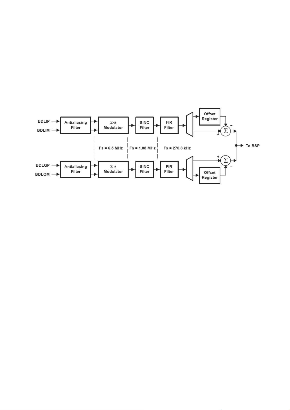
In order to process the analog base-band RXIP, RXIN, RXQP and RXQN generated by the
RF circuits to DSP U201 (Calypso-Lite), the BDL path of U202 (IOTA) includes two identical
Motorola Proprietary Information/
Page 7
W220 GSM/GPRS Level 3 Circuit Descriptions
725 Edge
circuits. The first stage of the BDL path is a continuous second-order ant-aliasing filter that
prevents aliasing of out-of-band frequency components due to sampling in the ADC. This filter
serves also as an adaptation stage between external and on-chip circuitry. The anti-aliasing
filter is followed by a fourth-order Σ - ∆ modulator that performs analog-to-digital
conversion at a sampling rate of 6.5 MHz. The ADC provides 2-bit words to a digital filter
that performs the decimation by a ratio of 24 to lower the sampling rate to 270.833 kHz. The
ADC also provides channel separation by providing enough rejection of the adjacent channels
to allow the demodulation performances required by the GSM specification. The BDL path
includes an offset register, in which the value representing the channel dc offset is stored. This
value is subtracted from the output of the digital filter before transmitting the digital samples
to the DSP via the BSP (Base-band Serial Port), i.e. BFSR on U202 Pin K11 and BDR on
U202 Pin L12.
Figure 4 BDL Function Diagram
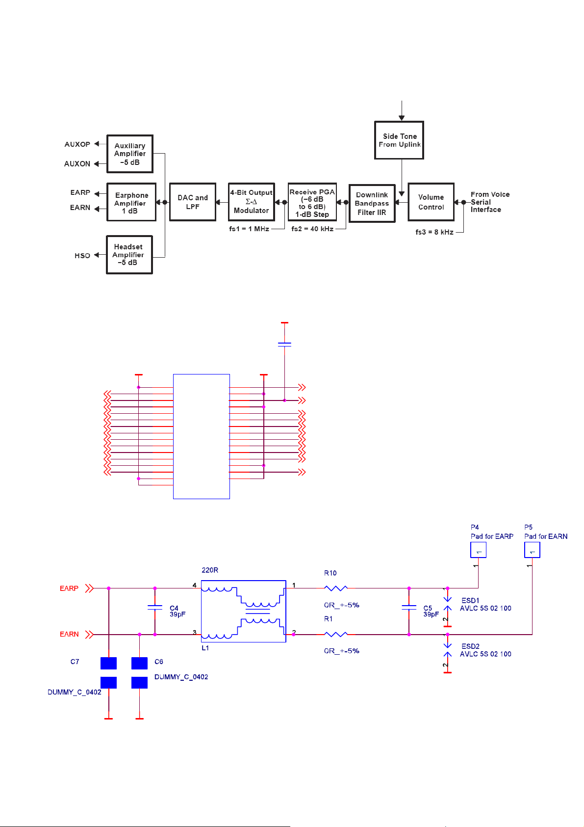
1.4 Audio
Internal to U202 (IOTA), in the voice downlink (VDL) path, the voice-band coder-decoder
(codec) (VBC) converts the digital samples of speech data received from the DSP via the
voice-band serial port VSP (VDX on Pin H10, VDR on Pin G12, VFSRX on Pin G11,
VCLKRX on Pin K12) into analog audio signals. The VBC includes an output amplifier of
headset and phone speaker. The VBC also performs the programmable gain, volume control,
and side-tone functions. In addition, the Audio Ringer signal will also be generated in the
U101 (Melody IC, ML2871) commanded by U201 (CalypsoLite).
The digital speech coming from the DSP is first fed to a speech digital filter that has two
functions. The first function is to interpolate the input signal and to increase the sampling rate
from 8 kHz up to 40 kHz to allow the digital-to-analog conversion to be performed by an over-
sampling digital modulator. The second function is to band-limit the speech signal with both
low-pass and high-pass transfer functions.
The interpolated and band-limited signal is fed to a second order Σ-∆digital modulator
sampled at 1 MHz to generate a 4-bit (9 levels) over-sampled signal. This signal is then passed
through a dynamic element-matching block and then to a 4-bit digital-to-analog converter
(DAC).
The volume control and the programmable gain are performed in the voice-band digital
filter. Volume control is performed in steps of 6 dB from 0 dB to −24 dB. In mute state,
attenuation is higher than 40 dB. A fine adjustment of gain is possible from −6 dB to +6 dB
in 1-dB steps to calibrate the system depending on the earphone characteristics. In fact, the
user can easily adjust the gain of the audio outputs with the volume control buttons.
Motorola Proprietary Information/
Page 8
W220 GSM/GPRS Level 3 Circuit Descriptions
725 Edge
The earphone amplifier provides a full differential signal on the EARP on Pin A12 and
EARN on Pin A11, and a headset output amplifier provides a single-ended signal on the
HSO on Pin A10.
Figure 5. VDL Function Diagram
1.4.1 Handset
VDD_1V8
LED1
VBAT
LED2
LED3
LCD_RESET
/WR
/RD
MAIN_CS
LED4
PWL
A0
1
1
3
3
5
5
7
7
9
9
11
11
13
13
15
15
17
17
19
19
21
21
23
23
25
25
27
27
29
29
31
31
31 pin connector
C1
33pF
U2
2
2
4
4
6
6
8
8
10
10
12
12
14
14
16
16
18
18
20
20
22
22
24
24
26
26
28
28
30
30
VIN_2V8
VBAT
D0
D1
D2
D3
D4
D5
D6
D7
EARNEARP
Figure 6. Earphone Path Circuit
Motorola Proprietary Information/
Page 9
W220 GSM/GPRS Level 3 Circuit Descriptions
725 Edge
U202 (IOTA)’s internal earphone differential amplifier (1dB) drives the handset speaker.
Following the Earphone path from EARP on Pin A12 and EARN on Pin A11, they are passed
trough Pin26 and Pin28 on CON301 to Pin27 and Pin28 on U2 respectively. They are routed
through and filtered by C4, L1 (Noise filter) and C5. Then, both voice signals respectively feed
into the P4 and P5. ESD1 and ESD2 are used to avoid ESD event.
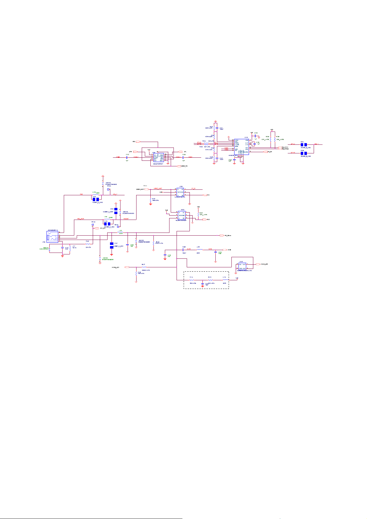
1.4.2 Headset
Figure 7. Audio Switching Path
The headset uses a standard 2.5mm phone jack. The jack contains a mechanical switch that
consists of J102 Pin 3 in serial with J102 Pin 4. As the headset device plug in, the switch path is
open. The voltage of EP_Status is changed from high (2.8V) to low (0V). The phone is
informed the headset device has been plugged in. The headset may contain a momentary
switch, which is normally closed. When the momentary switch is pressed, then U107 (2.2V
Reset IC) is triggered and the output Hook_SW on Pin 1 is set high. The phone will detect the
voltage variation and make an appropriate response to this action, which could be to answer a
call, end a call.
The Headset Speaker is driven by U202 (IOTA)’s internal headset amplifier. Following the
headset speaker path from the U202 (IOTA) Pin A10 HSO in parallel with C218 to filter out
high band noise, in serial with C121 to block DC and in parallel with R125, it is routed and
passed through U104 (Analog Switch), coming out with COM1 and COM2. Then, they are
routed into U105 (Headphone Amplifier). U105’s OUTL and OUTR are fed back into MAX
BASS OP Circuit consisting of internal OP and external resistors to set Max Gain, and then
are coming out with OP_L1 and OP_R1.
OP_L1 is directly connected to J102 Pin 6 in serial with L106 and in parallel with ESD113.
OP_R1 is routed into U104 (Analog Switch) Pin 1 and comes out from HSOOUT on Pin 4.
The signal is connected to J102 Pin 1 in serial with L101 and in parallel with ESD106.
Motorola Proprietary Information/
Page 10

W220 GSM/GPRS Level 3 Circuit Descriptions
725 Edge
1.5 26MHz System Clock
Figure 8. DCXO diagram
U604(Aero II SI4210) integrates the DCXO circuitry required to generate a precise system
reference clock using only an external crystal resonator. It is configured in DCXO mode by
tying XMODE Pin 25 high. The Pin 31 XTAL1 and Pin 30 XTAL2 are then connected directly
to the 26 MHz crystal.
A internal Buffer is available to provide a reference clock output from the XOUT on Pin 8 in
serial with C201 to U201 (CalypsoLite) Pin C16. The XOUT buffer is enabled when the XEN
pin is set high.
2 TRANSMIT
2.1 Audio
Internal to U202 (IOTA), the voice-band coder-decoder (codec) (VBC) circuit processes
analog audio components in the voice uplink (VUL) path.
The microphone amplifier has a gain of typically 25.6 dB (±1 dB) and provides an external
voltage of 2.0 V or 2.5 V to bias the microphone (MICBIAS).
The auxiliary (Headset microphone) audio input can be used as an alternative source for
higher-level speech signals. This stage performs single-ended to differential conversion and
provides a programmable gain of 4.6 dB or 28.2 dB.
The resulting fully differential signal is fed to the analog-to-digital converter (ADC). Analogto-digital conversion is performed by a third-order Σ-∆modulator with a sampling rate of 1
MHz. Output of the ADC is fed to a speech digital filter, which performs the decimation
down to 8 kHz and band-limits the signal with both low-pass and high-pass transfer
functions. Programmable gain can be set digitally from −12 dB to +12 dB in 1-dB steps. The
speech samples are then transmitted to the DSP via the VSP at a rate of 8 kHz.
Motorola Proprietary Information/
Page 11

W220 GSM/GPRS Level 3 Circuit Descriptions
725 Edge
Figure 9 VUL Path
2.1.1 Microphone
The Microphone is a single-end output type. The signal MICIP connected to ground and
MICIN is coming out from Pin 1 of U110. Both of them are sequentially in serial with C111
and C112 to block DC signal and then coming out as MICIP and MICIN into U202 (IOTA)
Pin D12 and Pin D11. Among them, MICIN is biased by MICBIAS_2 from U202 Pin C11.
And, MICBIAS_2 is coming from MICBIAS from U202 Pin C11 depended on Hall_Sensor
from U201 Pin K13.
MICBIAS
R141
100K/+-5%
U111
4
5
6
NTZD3155CT1G
D2
S2
G1
G2
S1
D1
Hall_Sensor
MICBIAS_2
3
2
1
R142
1M/+-5%
Figure 10 Microphone LC network
Motorola Proprietary Information/
Page 12

W220 GSM/GPRS Level 3 Circuit Descriptions
725 Edge
2.1.2 Mono Headset
The Headset Microphone is a 32ohm single-ended type. The received signal is fed into J102
Pin 4. Sequentially, it is routed in parallel with ESD107 and in serial with L102. Then it is
passed through U103 (Analog switch) Pin 4 and coming out from Pin 1. It is in serial with
C125 to block DC and L103 (Bead) to filter out high band noise and coming out AUXI into
U202 (IOTA) Pin E10.
Figure 11 Headset Microphone Path
2.2 Modulation
Internal to U202 (IOTA), the modulator circuit in the BUL path performs the Gaussian
minimum shift keying (GMSK). The data to be modulated flows from the DSP radio
interface (RIF) through the base-band serial port (BSP), i.e. BFSX on U202 Pin J9 and
BDX on U202 Pin M12.
The entire content of a burst, including guard bits, tail bits, and data bits, is stored in one
of two 160-bit burst buffers before starting the transmission. The presence of two burst
buffers is dictated by the need to support multislot transmission: one buffer is loaded with new
data while the content of the second buffer is pushed into the GMSK modulator for
transmission. When single-slot mode is selected, only the content of burst buffer 1 is used for
modulation.
The GMSK modulator is implemented digitally, the Gaussian filter computed on 4 bits of
the input data stream being encoded in the sine/cosine look-up tables in ROM, and it generates
the in-phase (I) and quadrature (Q) digital samples with an interpolation ratio of 16. These
digital I and Q words are sampled at 4.33 MHz and applied to the inputs of a pair of 10-bit
DACs. The analog outputs are then passed through third-order Bessel filters to reduce out-
of-band noise and image frequency and to obtain a modulated output spectrum.
Motorola Proprietary Information/
Page 13

W220 GSM/GPRS Level 3 Circuit Descriptions
725 Edge
To minimize phase trajectory error, the dc offset of I and Q channels can be minimized
using offset calibration capability. During offset calibration, input words of the 10-bit DACs
are set to zero code and a 6-bit sub-DAC is used to minimize the dc offset at analog outputs.
Fully differential signals are available at the BULIP (TXIP) on U202 Pin C4, BULIM
(TXIN) on U202 Pin A4, BULQP (TXQP) on U202 Pin A3, and BULQM (TXQN) on U202
Pin A3.
Figure 12. BUL modulation diagram
2.3 TX VCO
Figure 13. TX Path In Red Line
TXIP on U202 Pin C4, TXIN on U202 Pin A4, TXQP on U202 Pin A3, and TXQN on
U202 Pin C3 are routed into a simple RC low pass filter to reduce out of band noise. Then,
fully differential signals are fed into U604 (Aero II SI4210). Internal to U604, the transmit
section consists of an I/Q baseband upconverter, an offset phase-locked loop (OPLL), and
two output buffers that can drive an external PA U605 (RF3166).
A quadrature mixer upconverts the differential in-phase (BIP, BIN) and quadrature
(BQP, BQN) baseband signals to an intermediate frequency (IF) that is filtered and which is
used as the reference input to the OPLL.
Motorola Proprietary Information/
Page 14

W220 GSM/GPRS Level 3 Circuit Descriptions
725 Edge
The OPLL consists of a feedback mixer, a phase detector, a loop filter, and a fully
integrated TXVCO. Low-pass filters before the OPLL phase detector reduce the harmonic
content of the quadrature modulator and feedback mixer outputs. The OPLL requires no
external filtering to attenuate transmitter noise and spurious signals in the receive band. The
output of the transmit VCO (TXVCO) is a constant-envelope signal that reduces the problem
of spectral spreading caused by non-linearity in the PA. Additionally, the TXVCO benefits
from isolation provided by the transmit output buffers. This significantly minimizes any load
pull effects and eliminates the need for off-chip isolation networks. One output RFOL on Pin
15 is Low Band path for the GSM 900 (880–915 MHz) band and Another output RFOH on
Pin 16 is High Band path for the DCS 1800 (1710–1785 MHz).
2.4 TX PA
Sequentially, TXVCO output RFOL and RFOH are fed into U605 (RF3166) respectively in
serial with C611 and R603 (3dB attenuator), and C612 and R602 (3dB attenuator).
U605 (RF3166) is a power amplifier module with integrated power control and with 3
stages internal Amplifier. It is designed for use as the final RF amplifier in GSM900,
DCS1800 handheld digital cellular equipment and other applications in the 880MHz to
915MHz and 1710MHz to 1785MHz bands. It incorporates RFMD’s latest VBATT tracking
circuit, which monitors battery voltage and prevents the power control loop from reaching
saturation furthermore to minimize switching transients. In the meanwhile, U605 (RF3166) is
kept constant the gain in the first stage and the overall noise power is not increased when
decreasing output power.
The LB and HB outputs of U605 (RF3166) are then routed into individual T type matching
networks. Both of them later are fed into U607 (T/R Switch) Pin 1 and Pin 3 and coming out
from Antenna port on U607 Pin 10.
Due to the selection of LB and HB TX path, VC1 on U608 Pin 6 set high (2.8V) and VC2 on
U608 PIN 4 set low put the phone into TX Mode of GSM900. VC1 on U608 Pin 6 set low and
VC2 on U608 PIN 4 set high (2.8V) puts the phone into TX Mode of DCS1800.
Continuously, TX signals are passed through RF connecter and Antenna matching network
and radiated into the Air space.
2.5 TX PA Power Control
The output power of U605 (RF3166) is controlled by U202 (IOTA) APC (automatic power
control) signal. APC generates an envelope signal to control the power ramp up, power
ramp down, and power level of the radio burst. The APC structure is intended to support
single-slot and multislot transmissions with smooth power transitions when consecutive bursts
are transmitted at different power levels. The APC includes a DAC and a RAM, in which the
shape of the edges (ramp up and ramp down) of the envelope signals are stored digitally.
This envelope signal is converted to an analog signal by a 10-bit DAC at a rate of 2167 kHz.
This processor computes the shape of the ramp-up and ramp-down transitions of the
envelope signal from the value of the power level step and from the 16 coefficients of the
desired shaping filter, which are stored in a random access memory (APCRAM) with an
interpolation factor of 4. The power step is obtained by subtracting the content of the y-level
registers, which contain the previous power level from the x-level register the new power level.
The automatic power control RAM register includes 16 10-bit words. The 5 LSBs of each word
represent the coefficients of the ramp-up shaping filter, while the 5 MSBs represent the
Motorola Proprietary Information/
Page 15

W220 GSM/GPRS Level 3 Circuit Descriptions
725 Edge
coefficients of the ramp-down shaping filter. Ramp-up or ramp-down coefficient selection
depends on the sign of the power step to be done—ramp-up for positive step and ramp-down
for negative step. The sum of the coefficients is normalized and must be equal to 128 in the
case of X2 slope.
The shaping filter generates 16 steps for ramp-up and 16 steps for ramp-down. In order to
minimize image frequencies due to this sampling, a 4-time linear interpolation generates a
64-step signal at the input of the DAC.
Before being fed to the 10-bit DAC (DAC10), the content of the offset register is added to
the 10-bit words computed by the APC processor. This offset generates a voltage at APC
output at power on to set the RF power amplifier to its conduction threshold.
The output of the 10-bit DAC is finally sent to the APC output through the output
amplifier stage, which provides some low-pass continuous time filtering to smooth the APC
signal.
Figure 14 APC Generation
Motorola Proprietary Information/
Page 16

W220 GSM/GPRS Level 3 Circuit Descriptions
725 Edge
3 Baseband Processsor
Speaker
XTAL
32.768 KHz
26MHz
VoiceBand
Codec
BaseBand
Codec
IOTA
Power
Management
SIM
Head-Set
(Earphone Jack)
Radio Frequency Circuit
Receiver /
Microphone
Dual Analog
Switch(Audio)
Charger
SIM Card
Hall Sensor
Indicator
LED
Keypad
Keypad
Backlight
Vibrator
LCD
Backlight
LCD module
(CSTN)
FM Chip
Earphone Amp
MAX9723
Indicatior
Driver IC
LED
Driver IC
OKI
Melody IC
8 bit
DSP
LEAD2
Calypso
-Lite
ARM7TDMIE
Internal
SRAM
FLASH (64Mb)
+
PSRAM (16Mb)
3.1 Main Baseband Digital Processor - U201 (CalypsoLite)
U201 (CALYPSOLite) is a chip implementing the digital Base-band processes of a
GSM/GPRS mobile phone. This chip combines a DSP sub-chip (LEAD2 CPU) with its
program and data memories, a Micro-Controller core with emulation facilities (ARM7TDMIE),
internal 8Kb of Boot ROM memory, 2M bit SRAM memory, a clock squarer cell, several
compiled single-port or 2-ports RAM and CMOS gates.
The application of CALYPSOLite is the management of the GSM/GPRS Base-band
processes through the GSM layer 1, 2 and 3 protocols as described in the ETSI standard
with a specific attention to the power consumption in both GSM dedicated and idle modes,
and GPRS (class 12) capability.
Motorola Proprietary Information/
Page 17

W220 GSM/GPRS Level 3 Circuit Descriptions
725 Edge
Figure 15 CalypsoLite Internal Architecture block diagram
3.2 Baseband Analogue Coprocessor –U202 (IOTA)
U202 (IOTA) includes a complete set of Base-band functions that perform the interface and
processing of the following voice signals, the Base-band in-phase (I) signal and quadrature
(Q) signals, which support single-slot and multi-slot modes. The IOTA also includes
associated auxiliary RF control features, supply voltage regulation, battery charging
controls, and switch ON/OFF system analysis.
U202 (IOTA) interfaces with the digital Base-band device U201 (CalypsoLite), through a
digital Base-band serial port (BSP) and a voice-band serial port (VSP). The signal ports
communicate with a DSP core. A micro-controller serial port (USP) communicates with the
micro-controller core and a time serial port (TSP) communicates with the time processing
unit (TPU) for real time control.
A specific module is dedicated to support the 3V/1.8V SIM card interface. The module
includes the generation of the SIM card supply voltage as well as level shifters to adapt the
SIM card signal levels to the micro-controller I/O signal levels.
U202 (IOTA-TWL3025) also includes an on-chip voltage reference; under-voltage
detection and power-on reset circuits.
Motorola Proprietary Information/
Page 18

W220 GSM/GPRS Level 3 Circuit Descriptions
725 Edge
Figure 16 IOTA Block diagram
4 Displays
4.1 Color Display:
The WinTek LCM is a 130(RGB)*130 Color STN LCM with 3 White LED embedded
inside the module. The interface coming out from U201 (CalypsoLite) is summarized as blow,
LCDC_CS: Chip selection
LCDC_RESET: Reset Input
LCM_DC: Data or command selection
PS: Bus Interface mode selection
D[0..7]: 8-bit bi-directional data bus. 6800 mode is set now.
LED1~3: WLED power input
LEDGND: LED Ground
LCM_VDDIO: power supply for logic
VCI: power supply for DC/DC
Motorola Proprietary Information/
Page 19

W220 GSM/GPRS Level 3 Circuit Descriptions
725 Edge
LCDC_CS, LCDC_RESET, LCM_DC, D[0..7] are passed through a set of EMI filters
ESD331, ESD332, and ESD333 and then fed into CN301 to LCM.
Figure 17. LCM Interface
4.2 Display Backlights
C14
100pF
PWL
1uF X5R 0603
C12
VBAT
LED1A
LED2A
16K/+-5%
13
14
15
16
17
VIN
LED1
LED2
LED3
NC
R11
12
EN
ISET11GND
LED41NC2GND3C1P
10
9
C2P
VOUT
C1N
C2N
VIN
4
C10
470nF X5R
U3
RT9368PQV
8
7
6
5
C13
1uF X5R 0603
C11
470nF X5R
VBAT
Figure 18 LCM Backlight driver
U3 (WLED Driver) has 4 ports to drive 4 White LEDs. It’s controlled by PWL on U201
(CalypsoLite) Pin R8. In the LCM, there are only 2 WLED embedded inside.
Motorola Proprietary Information/
Page 20

W220 GSM/GPRS Level 3 Circuit Descriptions
0
725 Edge
4.3 Display Indicators
ESD304
AVNC 5S 05 Q 050
123
ESD301
B72590T0040M060
U313
LED2
1
2
3
4
5
IO0
IO1
IO2
IO3
VSS
PCA9537DP
LED1
LED3
LED4
45
678
1 2
VDD
SDA
SCL
/INT
/RESET
10
9
8
7
6
C345
100nF
V-IO
nRESET
R325
10K_+-5%
C349
DUMMY_C_0402
10K_+-5%
I2C_SDA
R326
C350
DUMMY_C_0402
10K_+-5%
I2C_SCL
12
R327
ESD302
B72590T0040M06
Figure 19 Indicator driver
U313 (4 bits I
2
C and SMBus low power I/O port) has 4 ports to drive 4 LEDs. It’s
controlled by I2C_SDA and I2C_SCL on U201 (CalypsoLite) PinT11 and PinT12
respectively.
5 32KHz RTC
Figure 20 32.768KHz Crystal
The Real-time Clock Interface is part of U201 (CalypsoLite) in use with the crystal X201.
The clock signal CLK32K_OUT is running on 32.768Khz as reference for the Clock module,
as deep sleep Clock and as the reference clock of U701 (FM Tuner).
6 SIM Circuit
The SIM Card digital interface in U202 (IOTA) insures the translation of logic levels
between U201 (CalypsoLite) and SIM card. The SIM card interface can be programmed to
drive a 1.8V or 3V SIM card.
Motorola Proprietary Information/
Page 21

W220 GSM/GPRS Level 3 Circuit Descriptions
725 Edge
The interfaces between SIM holder CON304 and U202 (IOTA) are summarized in the
following:
SIMCLK – SIM card reference clock
SIMRST – SIM card reset
SIMIO – SIM card bidirectional data line
VRSIM – power supply for SIM card
Figure 21 SIM Slot
7 Keypad
7.1 Keypad
The keypad keyboard is connected to the U201 (CalypsoLite) using:
KBR (4:0) - input pins for row lines
KBC (3:0) - output pins for column lines
If a key button of the keyboard matrix is pressed, the corresponding row and column lines are
shorted together. To allow key press detection, all input pins (KBR) are pulled up to VCC and
all output pins (KBC) are driving a low level. Any action on a button will generate an interrupt
to the micro-controller, which will scan the column lines with sequence.
Motorola Proprietary Information/
Page 22

W220 GSM/GPRS Level 3 Circuit Descriptions
725 Edge
KBR0
KBR1
KBR2
KBR3
KBR4
KBC0
KBC1
1
S1
KSW
[Send]
2
1
S5
KSW
[1]
2
1
S9
KSW
[4]
2
1
S13
KSW
[7]
2
1
S17
KSW
[*]
2
1
2
1
2
1
2
1
2
1
2
S2
KSW
[<=]
S6
KSW
[2]
S10
KSW
[5]
S14
KSW
[8]
S18
KSW
[0]
KBC2
1
2
1
2
1
2
1
2
1
2
S3
KSW
[Center]
S7
KSW
[3]
S11
KSW
[6]
S15
KSW
[9]
S19
KSW
[#]
KBC3
1
2
1
2
1
2
1
2
1
2
S4
KSW
[v]
S8
KSW
[^]
S12
KSW
[=>]
S16
KSW
[Left-Upper]
S20
KSW
[Right-Upper]
Figure 22 Keypad Matrix
7.2 Keypad Backlights
The keypad backlights are directly controlled on/ off by KeypadLED of U201 (CalypsoLite)
without any external LED driver. Backlight in serial with two resisters R402 and R403 is
directly supplied by the Battery Cells.
Motorola Proprietary Information/
Page 23

W220 GSM/GPRS Level 3 Circuit Descriptions
T
725 Edge
BACKLIGHT
12
LED1
SL3G-BXT
12
LED2
SL3G-BXT
12
LED3
SL3G-BXT
KeypadLED
12
LED4
SL3G-BXT
12
LED5
SL3G-BXT
12
LED6
SL3G-BX
Figure 23. Keypad LEDs
8 Memory
8.1 U501 – ST Microelectronics Memory M36W0R6040T1ZAQF
U501 (Flash memory and PSRAM) is used to store code and other parameters. It contains
64M-bit Flash memory and 16M-bit PSRAM. The power supply of Memory is listed as
below:
Flash Power Supply (F1-VCC) : 1.8V
Flash Output Buffer power supply (VCCQ) : 1.8V
SRAM Power Supply (P-VCC) : 1.8V
Flash Program Power Supply (F-VPP) : 1.8V
The control/communication signals are listed as below:
A[1..22] : Memory Address Lines
D[0..15] : Memory Data Lines
/RD : Active Low READ Signal
/WE : Active Low Write Signal
/CS0, /CS3 : Memory Chip Select Signal, Flash = /CS0, SRAM = /CS3
/BHE, /BLE : Low Byte /High Byte Buffer Enable Signal
Motorola Proprietary Information/
Page 24

W220 GSM/GPRS Level 3 Circuit Descriptions
725 Edge
A[1..22]
A[1..22]
100K/+-5%
R502
V-SRAM
R501
1K_+-5%
U501
WAIT
S-CS2
P-MODE
F3-CE#
P2-CS#
F-VPP,F-VPEN
S-VCC
P-VCC
VCCQ
VCCQ
VCCQ
CLK
D10
D11
D12
D13
D14
D15
VSS
VSS
VSS
VSS
VSS
VSS
VSS
VSS
C6
G7
C5
K8
K3
K2
D0
H2
D0
D1
H3
D1
D2
G3
D2
D3
H4
D3
D4
J5
D4
D5
G5
D5
D6
J6
D6
D7
H7
D7
D8
G2
D8
D9
J3
D9
D10
G4
D11
J4
D12
H5
D13
G6
D14
H6
D15
J7
M1
DU
M2
DU
M7
DU
M8
DU
A1
DU
A2
DU
A7
DU
A8
DU
V-FLASH
D4
K4
K5
B4
C4
L1
L2
L5
L6
L7
L8
L3
J8
K7
C506
100nF
V-FLASH
C501
100nF
V-SRAM
C502
100nF
D[0..15]
D[0..15]
/RD
FDP
/BHE
/BLE
/WE
/CS3
/CS0
/RD
/RD
V-FLASH
V-FLASH
FDP
/BHE
/BLE
/WE
/CS3
/CS0
/RD
C505
100nF
A1
A2
A3
A4
A5
A6
A7
A8
A9
A10
A11
A12
A13
A14
A15
A16
A17
A18
A19
A20
A21
A22
G1
A0
F1
A1
E1
A2
D1
A3
B1
A4
C1
A5
F2
A6
E2
A7
F6
A8
D7
A9
E7
A10
B8
A11
C8
A12
D8
A13
F7
A14
E8
A15
F8
A16
D2
A17
B2
A18
B3
A19
E6
A20
B7
A21
C7
C3
D3
E3
H1
F4
F3
C2
D5
D6
E5
E4
F5
K1
G8
J2
H8
J1
L4
B5
K6
B6
PF38F2030W0YTQE
A22
A23
A24
A25
R-OE#
F-RST#
R-UB#
R-LB#
R-WE#
P1-CS#
ADV#
F-WP#
F-WE#
F1-CE#
F2-CE#
F1-OE#
F2-OE#
S-CS1#
F1-VCC
F1-VCC
F2-VCC
F2-VCC
Figure 24. ST Microelectronics 64Mb NOR Flash + 16 Mbit PSRAM
9 Charging Circuit and External Power
We can obtain power from 2 sources, from either the battery or from an external charger /
Power source via the accessory connector to support Baseband.
9.1 Battery support
V-IO
R301
Battery connector
302_4P_0422
4
3
2
1
CON302
4
3
2
1
BAT_ID
BAT_TEMP
5.1K/+-5%
ESD328
1uF
MVBAT
BAT_ID
BAT_TEMP
Figure 25. Battery Cell supply
The Battery CON302 is made up of 4 pins, these are
♦ Pin4-MVBAT, it supplies whole system power.
♦ Pin3-BAT_ID, but now it’s dummy function.
C323
33pF
MVBAT
C324
10pF
C337
3.9pF
Motorola Proprietary Information/
Page 25
W220 GSM/GPRS Level 3 Circuit Descriptions
725 Edge
♦ Pin2-BAT_TEMP, Used to measure the Battery temperature during charging, fed into
Pin E3 on U202 (IOTA). As charging, Battery temperature arise over 45 and then BB
will stop charging immediately to protect overall system.
♦ Pin1-GND
9.2 Charger support
CON303
C-PJK15-00-00
4
3
2
1
R317
18K/+-1%
D301
MMSZ5256BT1G
A C
PST414L400UR
U310
13K/+-1%
1
GND
VDD
3
VDC_IN
5
VCC
4
NCP345SNT1G
R309
2
RESET
510K/+-5%
U304
OUT
GND
CNTRL3IN
R304
1
2
1
2
3
4
AAT4610AIJS-1-T1
R320
1K/+-5%
VDC_IN_1
1278345
U306
8
SET
GND
7
/ON
GND
6
5
6
U308
NTHD4102PT1G
R307
DUMMY_R_0402
U302
A C
CRG03(TE85L,Q,M)
R321
1K/+-5%
IN
GND
IN
OUT
C343
470nF
R303
0.2/+-0.5%
C313
22nF
VCHG
MVBAT
VCCS
VBATS
VBAT
U301
2
RESET
1
GND
PST414L438UR
MVBAT
VDD
VCHG
MVBAT
R306
100K/+-1%
R311
62K/1%
ICTL
3
3
Drain
Gate1Source
VCHG
U303
SSM3K16TE(TE85L,F)
2
Figure 26. Charging Circuit
9.2.1 Charging Current Path
As the charger unit plug in, charging current flows into U308 (PMOS) and then is passed
through U306 (Over-current limiter). In order to avoid the reverse current fed back into a
charger, U302 (rectifier diode) is applied. The charging current is passed through it and fed into
VBAT, which is mainly supplying U202 (IOTA) regulated power. Later, the charging current
enters U308 (PMOS) again with ICTL to control the charging current Level. ICTL is a
current control signal from Battery charging interface of U202 (IOTA). And then, the
charging current in serial with R303 is fed into MVBAT to charge the really battery cell.
9.2.2 Protection Mechanism of charging circuits
The Charging Protection mechanism is compliant with MOTOROLA safety technical
specification. Its fundamental concept is to avoid the battery cell burning by overcharging or
damaging all system by overvoltage inrush.
To avoid 45V Overvoltage inrush in a short period, we add D301 to bypass it. To avoid
over-6.8V changer inrush, we add U304 (Overvoltage protector) to guard there. As the event
of plugging in over-6.8V charger happens, U304 (Overvoltage protector) pulls up its Pin 1 to
close the channel of U308 (PMOS) to disconnect the charging path.
By the way, Pin 1 can be externally controlled by Pin 3, which is now routed with U301
(Reset IC). As the battery cell voltage is charging over 4.38V, U301 will arise its output Pin 2
to trigger U304 (Overvoltage protector) to pull up U304 Pin 1 as well.
To avoid Overcurrent charging, U306 (Over-current limiter)
is set to limit the charging
current as 600mA by pulling down U306 Pin 1 in serial with R309 (13Kohm).
MVBAT_ADC
Motorola Proprietary Information/
Page 26

W220 GSM/GPRS Level 3 Circuit Descriptions
725 Edge
10 MELODY IC
10.1 U101 - OKI ML2871
D[0..7]
R101
C101
R103
68K_+-5%
130K/+-5%
100pF
0.1uF
D0
D1
D2
D3
D4
D5
D6
D7
V-FLASH
C134
C104
0.1uF
C109
1uF
U101
B3
AOUT
A3
MIXIN
B4
MIXOUT
E4
D0
F5
D1
F6
D2
E5
D3
E6
D4
D6
D5
D5
D6
D4
D7
C1
NC
C2
NC
A1
VREF
F2
IOVDD
C3
SPGND
C4
SPGND
C5
SPGND
ML2871
SPOUT+
SPOUT-
DGND
DVDD
CLKI
SPVDD
SPGND
WR
IRQ
RST
IFSEL
A6
B6
B2
B1
F1
E1
P0
A5
NC
A4
B5
C6
P5
F4
F3
CS
E3
ILE
E2
RD
D2
D1
D3
A2
NC
V-IO
C105
0.1uF
CLK13M_OUT
/WE
/CS1
A1
/RD
/MELODY_RESET
Speaker_P
Speaker_N
ESD109
CLK13M_OUT
/WE
/CS1
A1
/RD
/MELODY_RESET
Speaker_P
Speaker_N
C102
4.7uF
MVBAT
C103
DUMMY_C_0402
V-IO
DUMMY_C_0402
Figure 27. Melody IC Circuit
U101 (OKI ML2871) is a synthesizer LSI for mobile phone that realizes advanced game
sounds designed for driving the speaker of the mobile. The power supply is listed as below:
Digital Power Supply (DVDD) : 1.8V
Digital Power Supply (IOVDD) : 1.8V
Analog Power Supply (SPVDD) : 3.2~4.2V
The control/communication signals are listed as below:
A1 : Memory Address Lines
D[0..7] : Memory Data Lines
/RD : Active Low READ Signal
/WE : Active Low Write Signal
/CS1 : Memory Chip Select Signal
CLK13M_Out : Melody IC Clock Input Signal
/Melody_Reset : Hardware RESET Melody IC Signal
The Analog Output Signals are listed as below:
Speaker_P : Differential + Speaker Output
Speaker_N : Differential – Speaker Output
Both of them are filtered out the high band noise repsectively in parallel with C309 and C308
and in serial with dual channel L31. To avoid ESD event, ESD303 is guard. Then, Both are
passed to CN305 and sound the speaker.
Motorola Proprietary Information/
Page 27

W220 GSM/GPRS Level 3 Circuit Descriptions
725 Edge
11 FM TUNER
11.1 FM IC – Philips TEA5761HN
Figure 28. FM IC Function Block
The U701 (TEA5761HN) integrates the complete tuner function from antenna input to stereo
audio output for FM broadband reception.
The power supply is listed as below:
Digital Power (VDD) : 2.8V
Digital Reference Voltage for Bus-Interface (V
Analog Power (VCC) : 2.8V
The control/communication signals are listed as below:
BUS_EN : Active Low Series Bus Enable Signal.
FM_GPIO1 : I2C Clock Signal.
FM_GPIO2: I2C Data Signal.
The Analog signals are listed as below:
AFL : FM Left Channel Audio Output.
AFR : FM Right Channel Audio Output.
ANT_FM : FM Antenna Signal Input.
The FM radio signal is received by using Headset itself as Antenna. The received signal is
fed back from J102 into the matching C707. However, C708 is used to block DC. The receiver
uses a digital low-IF architecture. The RX section integrates a low noise amplifier (LNA)
REFDIG
) : 2.8V
Motorola Proprietary Information/
Page 28

W220 GSM/GPRS Level 3 Circuit Descriptions
725 Edge
supporting the FM broadcast band (76 to 108 MHz). An automatic gain control (AGC)
circuit controls the gain of the LNA and PGA blocks to optimize for sensitivity and rejection
of strong interferers.
A quadrature image-reject mixer downconverts the RF signal to low-IF. The mixer output
is amplified and then digitized with high resolution analog-to-digital converters (ADCs).
Digital circuitry is used to perform channel selection, FM demodulation, stereo MPX
processing. High-fidelity stereo 16-bit digital-to-analog converters (DACs) drive analog
audio signals onto the LOUT as AFL and ROUT as AFR.
11.2 Audio Multiplex
AFL and AFR are routed and passed through U104 (Analog Switch), coming out with
COM1 and COM2. Then, they are routed into U105 (Headphone Amplifier). U105’s OUTL
and OUTR are fed back into MAX BASS OP Circuit consisting of internal OP and external
resisters to set Max Gain, and then are coming out with OP_L1 and OP_R1.
OP_L1 is directly connected to J102 Pin 6 in serial with L106 and in parallel with ESD113.
OP_R1 is routed into U104 (Analog Switch) Pin 1 and comes out from Pin 4 HSOOUT
signal is fed to J102 Pin 1 in serial with L101 and in parallel with ESD106.
. The
Figure 29 Audio Path
Motorola Proprietary Information/
Page 29

W220 GSM/GPRS Level 3 Circuit Descriptions
725 Edge
12 HALL SENSOR
The Hall Sensor is activated via turning on the U109 by magnetism. The output from U109,
Pin1 (Hall_Sensor), goes to Pin K13 of U201 (CalypsoLite). The driving supply power directly
comes from the real battery VIO.
V-IO
R111
56K/+-5%
Hall_Sensor
C143
10pF
1
OUTPUT
2
NO CONNECTION
3
GROUND
SUPPLY
NO CONNECTION
GROUND
6
5
4
C142
100nF
U109 A3212EEHLT-T
Figure 30 Hall Sensor
13 VIBRATOR MOTOR
The Vibrator Motor is activated via turning on a U312 (Transistor) with control signal,
VIBRATOR_ON from Pin H13 of U201 (CalypsoLite). The driving supply power directly
comes from the real battery MVBAT.
MVBAT
VIB1
SX-YKL-NZ3XK-0B
+1-
2
C347
DUMMY_C_0402
C348
DUMMY_C_0402
VIBRATOR_ON
R324
10K_+-5%
R323
20/+-5%
U312
1
GATE
DRAIN
2
SOURCE
NTA4001NT1G
R322
20/+-5%
3
Figure 31 Vibrator
Motorola Proprietary Information/
 Loading...