

Page 1
W215/W218
Level 3
Circuit Description
25 April 2007
V1.0
Page 2

W215/W218 Level 3 C
Index
1 Receive.................................................................................................... 4
1.1 Band selection........................................................................................... 4
1.2 Demodulation............................................................................................ 5
1.3 Audio Codec.............................................................................................. 6
1.3.1 Voice Downlink Patch.................................................................................................. 7
1.4 Earpiece Receiver ...................................................................................... 7
1.5 Headset.................................................................................................... 7
1.6 Speaker Phone .......................................................................................... 7
1.7 Data Download Receive Path...................................................................... 8
2 Transmit .................................................................................................. 8
2.1 Audio (Voice uplink Patch)..........................................................................
2.2 Data Download Transmit Path ....................................................................
2.3 Stereo Audio Path......................................................................................
2.4 Modulation
2.5
RF TX PA
2.6
TX PA Power Control in SKY77318
3 Triton-Lite Monitoring ADC ....................................................................14
4 Baseband Serial Port (BSP)....................................................................15
................................................................................................................... 10
...............................................................................................
..........................................................
9
9
9
12
13
5 Microcontroller Serial Port (USP)...........................................................15
6 General purposes I/O (GPIO).................................................................15
7 TFT LCD Display......................................................................................17
7.1 Display Backlights
...................................................................................................... 18
7.2 Image Processor ...................................................................................... 18
7.3 Camera Module........................................................................................ 19
8 32kHz RTC..............................................................................................19
9 SIM Card Circuit .....................................................................................19
9.1 SIM Card Supply Voltage Generation......................................................... 20
10 Keypad...................................................................................................20
10.1 Keypad Matrix ......................................................................................... 21
11 Vibrator circuit .......................................................................................21
Motorola Proprietary Information
- 2 -
Page 3

W215/W218 Level 3 C
12 Memory ..................................................................................................21
13 Power .....................................................................................................22
13.1 Low-Dropout Voltage Regulators...............................................................
13.2 Power Down Methods ..............................................................................
14 Sleep Module ..........................................................................................23
14.1 Sleep Up Sequence..................................................................................
14.2 Sleep off Sequence..................................................................................
15 Power Tree .............................................................................................25
16 Charging Circuit and External Power .....................................................25
16.1 Battery Support.......................................................................................
16.2 Charger Support......................................................................................
22
23
24
24
25
25
Motorola Proprietary Information
- 3 -
Page 4
W215/W218 Level 3 C
1 Receive
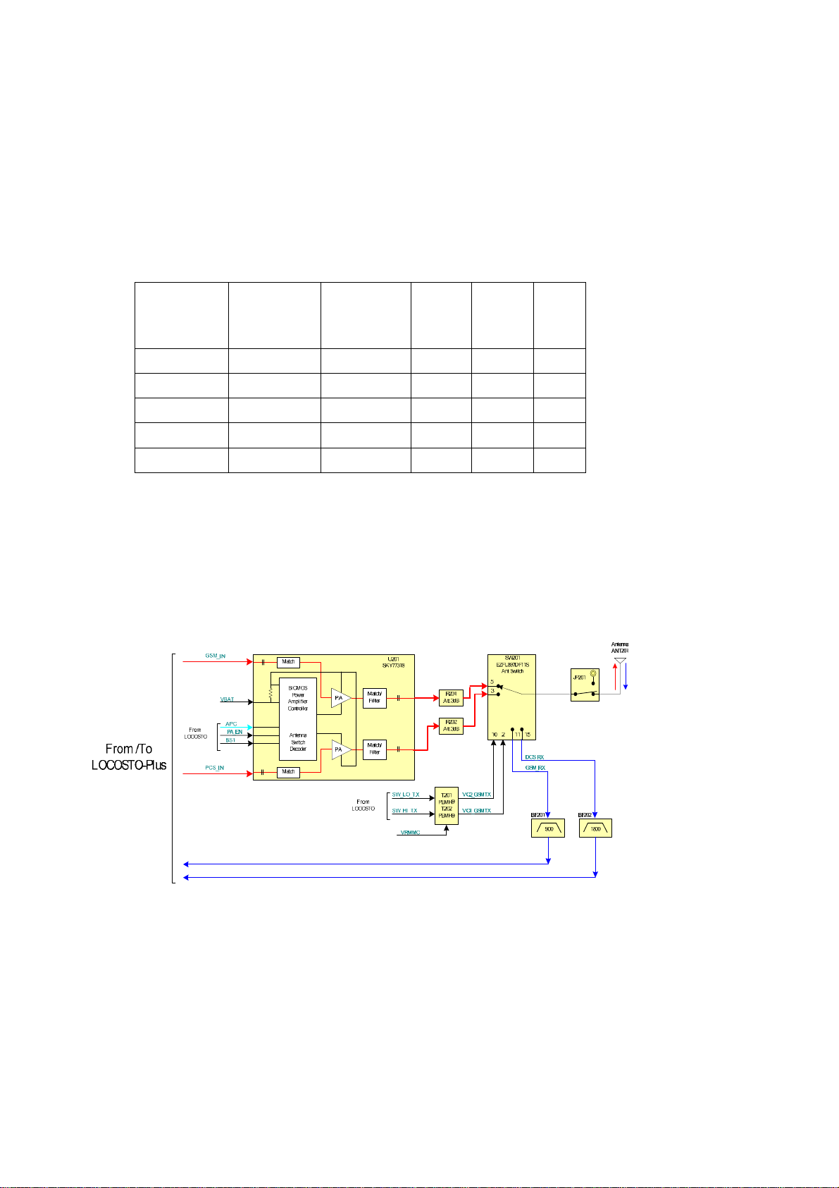
1.1 Band selection
The radio frequency signal is received from internal PIFA-type antenna. Received
GSM RF signal enters to PCB through the RF switch JP201. At this moment the T/R switch
SW201 is switched to RX mode to let the signal input to next stage. Then the signal goes
into SAW filter, BF201 and BF202 , which reject out-band signal and transfer the signal
from single-end to balanced. And the matching circuits between T/R switch and SAW
filter reduce the unwanted RF signal reflection and provide a flat frequency response in the
operation band. Finally the received signal will fed into Locosto Plus U101 DRP core
through a balanced MLCC matching network. The following table describes the control
voltages of T/R switch and PA:
SW_LO_TX
W215
Standby Low x Low Low x
RX EGSM900 Low Low Low Low Low
RX DCS1800 Low Low Low Low High
TX GSM900 High High High High Low
TX DCS1800 High High High High High
The RF signal is received by internal antenna or by RF plug, and the signal is passing
through the RF switch JP201 and then fed into T/R switch. The low band (GSM900) RX
received signal is transmitted from SW201 (Pin 11) and input to low-band SAW filter
BF201, while the high band (DCS1800) RX received signal from SW201 (Pin 1) and then
input to high-band SAW filter BF202. The last stage of RX on PCB is Locosto U101
(Loocsto-Plus), and the DRP process will make the signal into binary data.
PIN 5
of T201
SW_HI_TX
PIN 2
of T201
PA_EN
TP201
VAPC
PIN 20
of U201
BS1
TP202
Figure 1: Locosto TX/RX Paths Description
Motorola Proprietary Information
- 4 -
Page 5
W215/W218 Level 3 C
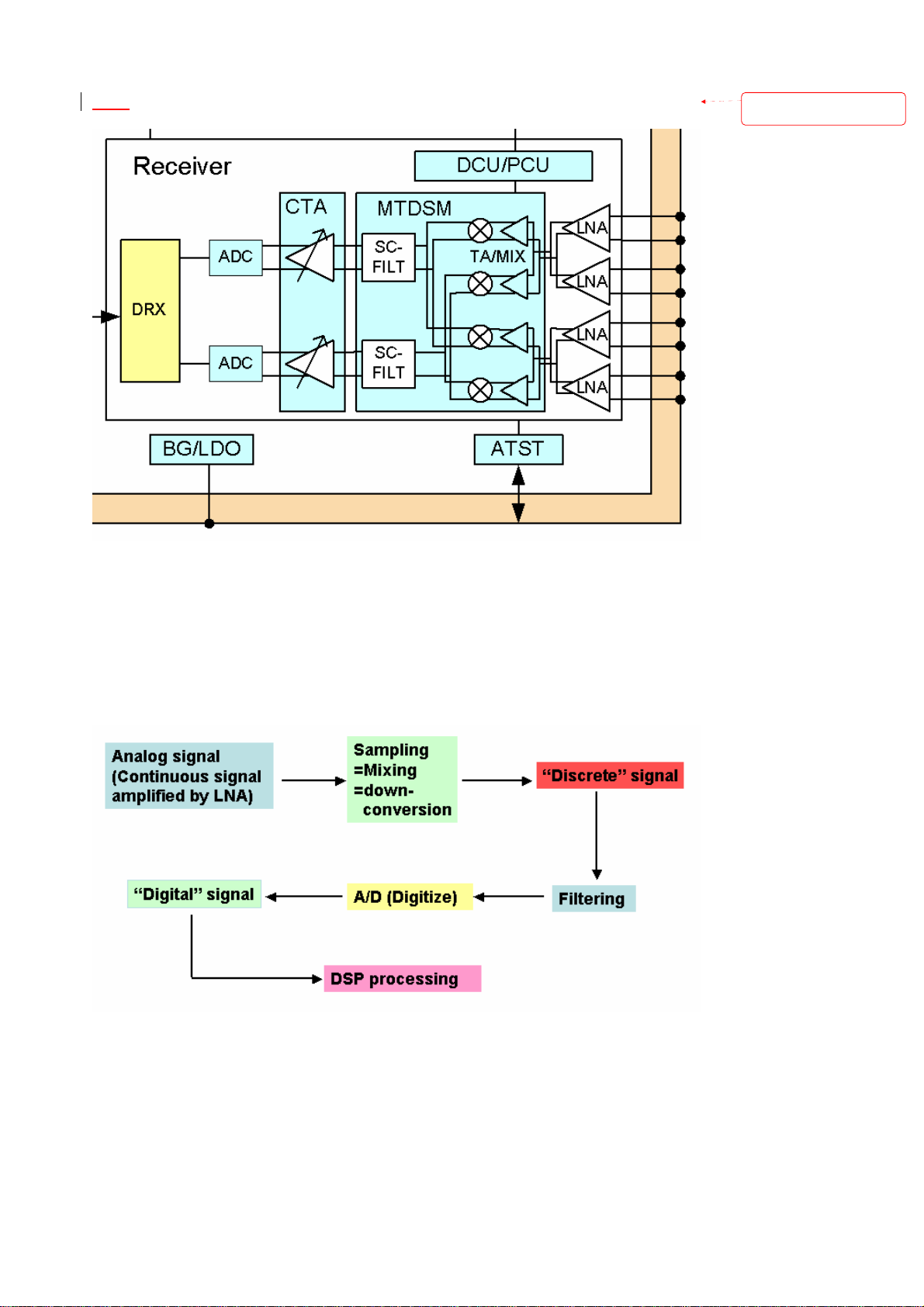
Locosto RX Mode
1.2
Formatiert:
und Aufzählungszeichen
Nummerierung
Figure 2: Locosto RX Signal Process
As described in Figure 2, when the RF signal is input to Locosto, it will be amplified by
a differential LNA in advance, in order to obtain a better NF in the last receiving stage.
And then it will be turned into discrete IF signal by a high-speed mixer. After passing
through a filter and an A/D converter, the discrete signal will become digital signal and
then input to Locosto core to do DSP process. The detail RX signal route is depicted as
below:
Motorola Proprietary Information
- 5 -
Page 6
W215/W218 Level 3 C
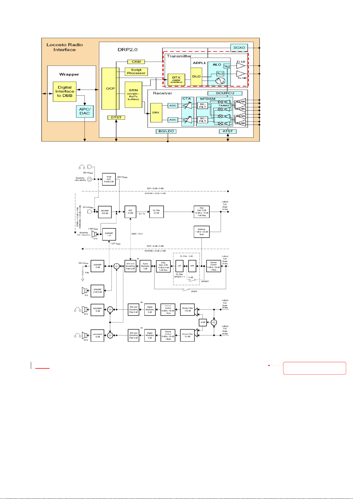
Figure 3: Baseband Downlink Block Diagram
Figure 3: Audio Codec Block Diagram
1.3
Audio Codec
The Audio codec consist of a voice codec dedicated to GSM application and an audio stereo
line. The voice codec circuitry processes analog audio components in the uplink path and
Motorola Proprietary Information
- 6 -
Formatiert:
und Aufzählungszeichen
Nummerierung
Page 7

W215/W218 Level 3 C
applies this signal to the voice signal interface for eventual baseband modulation. In the
downlink path, the codec circuitry changes voice component data received from the voice
serial interface into analog audio. The voice codec support an 8/16 kHz sampling
frequency. The stereo audio path converts audio component data received from the I2S
serial interface into analog audio. The following paragraphs describe these
uplink/downlink and audio stereo functions in more details.
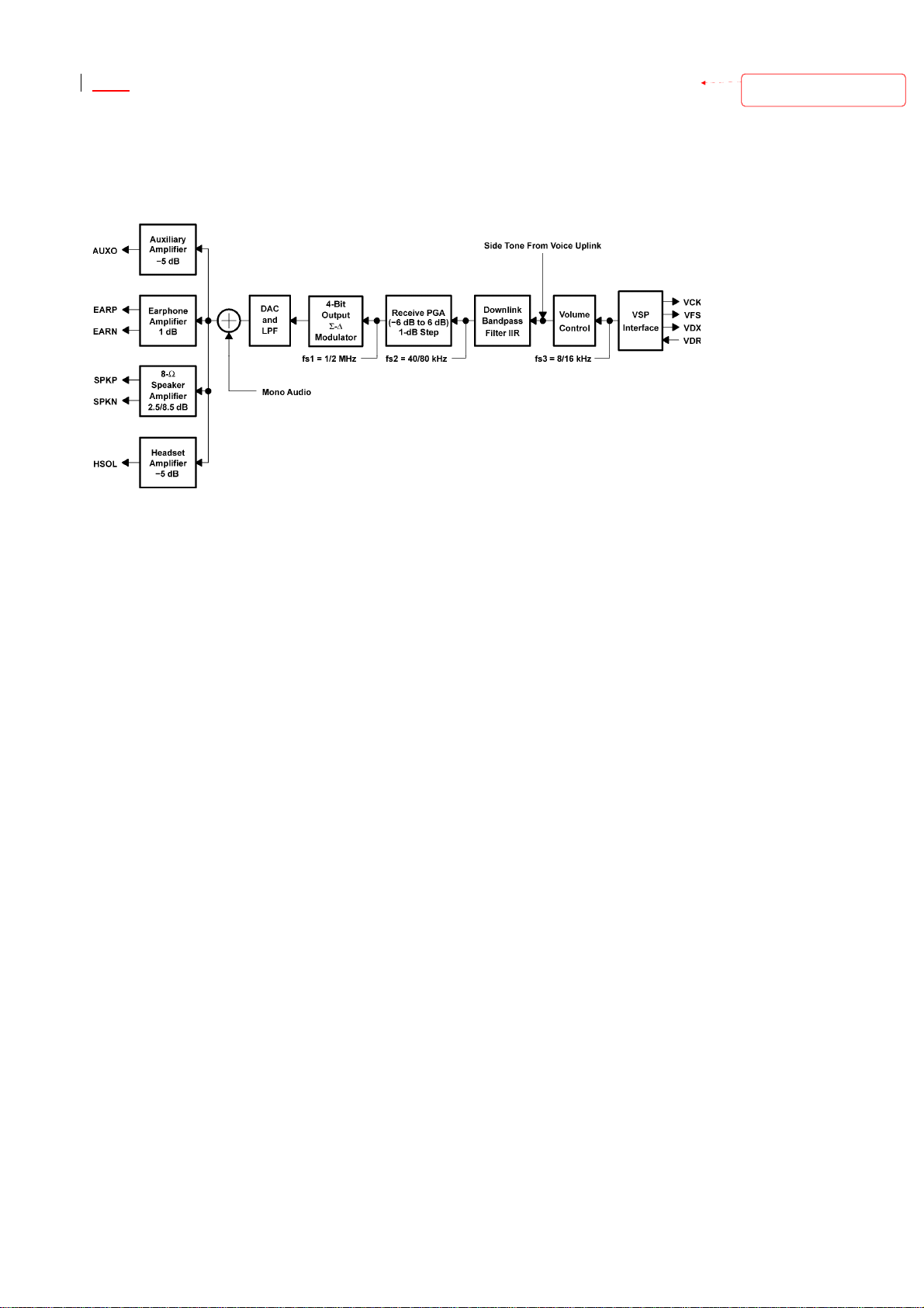
1.3.1 Voice Downlink Patch
The VDL path receives speech samples at the rate of 8 kHz from the Locosto-Plus IC U101
(DSP) via the VSP and converts them to analog signals to drive the external speech
transducer.
The digital speech coming from the Locosto-Plus IC U101 (DSP) is first fed to a speech
digital filter that has two functions. The first function is to interpolate the input signal and
to increase the sampling rate from 8 kHz up to 40 kHz to allow the digital-to-analog
conversion to be performed by an over-sampling digital modulator. The second function is
to band-limit the speech signal with both low-pass and high-pass transfer functions. The
filter, the PGA gain, and the volume gain can be bypassed by programming.
The interpolated and band-limited signal is fed to a second order Σ-∆ digital modulator
sampled at 1 MHz to generate a 4-bit (9 levels) over-sampled signal. This signal is then
passed through a dynamic element-matching block and then to a 4-bit digital-to-analog
converter (DAC).
Due to the over-sampling conversion, the analog signal obtained at the output of the 4–bit
DAC is mixed with a high frequency noise. Because a 4–bit digital output is used, a
first–order RC filter (included in the output stage) is enough to filter this noise.
The volume control and the programmable gain are performed in the TX digital filter.
Volume control is performed in steps of 6 dB from 0 dB to -24 dB. In mute state,
attenuation is higher than 40 dB. A fine adjustment of gain is possible from -6 dB to +6 dB
in 1–dB steps to calibrate the system depending on the earphone characteristics. The
earphone amplifier provides a full differential signal on the terminals EARP Triton-Lite Pin
J2 and EARN Triton-Lite Pin H2. The 8Ohm speaker amplifier provides a differential
signal on the terminals SPKP Triton-Lite Pin L6, K6 and SPKN Triton-Lite Pin M6, M7.
1.4
Earpiece Receiver
The Receiver J10 is connected to EARP Triton-Lite Pin J2 and EARN Triton-Lite Pin H2.
Headset
1.5
The headset uses a standard 2.5mm phone jack. The headset circuit contains analog
switches (U602 and U605), which are normally switched to receiver earpiece after power
on. When system turns on, the signal HS_EN (U101 Pin T3) are applied. When earphone
plug in, the phone will detect this action and make an appropriate response to answer a
call while incoming call occur. The interrupt for the headphones is detected on the
HS_DETECT (U101 Pin C6) line from Pin 6 of Headset Jack J602. This signal will be
pulled to high when the headset is connected.
1.6
Speaker Phone
When the handset set the hand-free mode, the Triton-Lite will switch from EARP/EARN
to SPKP/SPKN trace and receiver signal will be through Audio amplifier U601 to Speaker.
Motorola Proprietary Information
- 7 -
Formatiert:
und Aufzählungszeichen
Formatiert:
und Aufzählungszeichen
Formatiert:
und Aufzählungszeichen
Nummerierung
Nummerierung
Nummerierung
Page 8
W215/W218 Level 3 C
Data Download Receive Path
1.7
The External download cable is connected to the Earphone Jack J602, the headset
connector of the mobile phone. The download path is routed from J602 Pin 2 via U602
Pin 1 and U607 Pin C1 to RX_Modem. The RX_Modem signal connects to
Locosto-Plus IC U101 Pin L7 to provide this capability. When software is set to download
mode, the signal HS_EN (U101 Pin T3) is applied high, the phone will entered to
download state till download cable pulls out.
Figure 4: Voice Codec Downlink Patch
Formatiert:
und Aufzählungszeichen
Nummerierung
2 Transmit
2.1 Audio (Voice uplink Patch)
The VUL path includes two input stages. The first stage is a microphone amplifier,
compatible with electric microphones containing a FET buffer with open drain output. The
microphone amplifier has a gain of typically 25.6 dB (±1 dB) and provides an external
voltage of 2.5V to bias the microphone (HS_BIAS Locosto-Plus Pin K8).
The auxiliary audio input can be used as an alternative source for higher-level speech
signals. This stage performs single-ended conversion and provides a programmable gain
of 4.6 dB or 28.2 dB. The third stage is a headset microphone amplifier, compatible with
electric microphones. The headset microphone amplifier has a gain of typically 18 dB and
provides an external voltage of 2.0V or 2.5V to bias the headset microphone (HS_BIAS
Locosto-Plus Pin K8). When one of the input stages (HSMIC) is in use, the other input
stages are disabled and powered down.
The resulting fully differential signal is fed to the analog-to-digital converter (ADC). The
ADC conversion slope depends on the value of the internal voltage reference.
Analog-to-digital conversion is performed by a third-order Σ-∆ modulator with a sampling
rate of 1 MHz. Output of the ADC is fed to a speech digital filter, which performs the
decimation down to 8 kHz and band-limits the signal with both low-pass and high-pass
transfer functions. Programmable gain can be set digitally from –12 dB to +12 dB in 1-dB
steps. The speech samples are then transmitted to the Locosto-Plus IC U101 via the VSP
at a rate of 8 kHz. There are 15 meaningful output bits.
Programmable functions of the VUL path, power-up, input selection, and gain are
Motorola Proprietary Information
- 8 -
Page 9

W215/W218 Level 3 C
controlled by the Baseband serial port (BSP) or the MCU serial port (USP) via the serial
interfaces. The VUL path can be powered down by Program.
Figure 5: Voice Uplink Paths
2.2 Data Download Transmit Path
The External download cable is connected to the Earphone Jack J602 Pin 3, the headset
connector of the mobile phone. The download path is routed from J602 Pin 3 via U605
Pin 1 and U608 (Level shifter) Pin C2 to TX_Modem. The TX_Modem signal connects
to Locosto-Plus IC U101 Pin P3 to provide this capability. When software is set to
download mode, the signal HS_EN (U101 Pin T3) is applied low, the phone will entered to
download state till download cable pull out.
2.3 Stereo Audio Path
The stereo audio path receives Left and right signal samples at the rate of a programmable
frequency, from 8kHz to 48kHz, via the I2S serial interface and converts them to analog
signals to drive the external audio signal or speech transducers.
The digital audio signal is first fed to an audio digital filter that has two functions. The first
function is to interpolate the input signal and to increase the sampling rate to allow the
digital–to–analog conversion to be performed by an over-sampling digital modulator. The
second function is to band–limit the audio signal with a low–pass transfer functions. The
interpolated and band–limited signal is fed to a second order Σ-∆ digital modulator
sampled at fS1 frequency to generate a 4–bit (9 levels) over-sampled signal. This signal is
then passed through a dynamic element matching block and then to a 4–bit
digital–to–analog converter (DAC).
Due to the over-sampling conversion, the analog signal obtained at the output of the 4–bit
DAC is mixed with a high frequency noise. Because a 4–bit digital output is used, a
first–order RC filter (included in the output stage) is enough to filter this noise.
Motorola Proprietary Information
- 9 -
Page 10

W215/W218 Level 3 C
The volume control is performed in the audio digital filter. Volume control is performed in
steps of 1 dB from 0 dB to -30 dB. In mute state, attenuation is higher than 40 dB. The
gain is independently programmable on the Left and Right channels, using the same
register VAUSCTRL. A common adjustment of gain is possible at 0dB or +6dB. A digital
Left/Right summer and 6dB attenuator allows output of a mono audio path. These
configurations are programmed with the register VAUDCTRL.
The Left and right head set amplifiers provide the stereo signal on terminals HSOL (U103
Pin G1) and HSOR (U103 Pin F1). The mono audio signal may be provided on the Right
or the Right and Left headset outputs. The mono audio signal may be sum to the speech
signal and provided on the Auxiliary, Earphone and/or 8Ohm Speaker outputs. The Audio
Stereo/Mono path can be powered down and configure with the PWDNG, VAUDCTRL and
VAUDPLL registers.
Figure 6: Stereo Audio Path
2.4 Modulation
As illustrated in Figure 7, GMSK 0.3 is generated with Gaussian low-pass filtered
bipolar data, applied to a DC coupled FM modulator, set to a modulation index of 0.5.
Figure 7: GMSK Modulation
2.4.1
Transmit Section
As compared with a traditional VCO, TI takes advantage of DCO scheme to design the
Motorola Proprietary Information
- 10 -
Formatiert:
und Aufzählungszeichen
Nummerierung
Page 11

W215/W218 Level 3 C
main TX oscillator in Locosto. DCO stands for “digitally controlled oscillator”, which uses
some digital switched capacitances to do frequency tuning, but it should be noticed that
the oscillator core is still analog. And Locosto DRP uses ADPLL (all digital phase lock loop)
architecture to design a digital synthesizer, and its reference frequency is provided by
26MHz DXCO. The ADPLL output signal will be pre-amplified by a digital controlled
pre-PA and then fed into PA module. The TX signals output at TXLB Locosto Plus Pin
F17 (low-band) and TXHB Locosto Plus Pin G17 (high-band).
Figure 9: Locosto Transmit Block Diagram
2.4.2 Digitally- Contr olled Crystal Oscillator (DCXO)
The DCXO system comprises an external crystal Y101, DCXO core based on Colpitts
oscillator, a switching capacitor array, amplitude control loop and a current DAC. It also
includes a startup system to control the startup sequence of the bandgap reference and
the LDO voltage regulator for the DCXO that is based on a 32 KHz clock. DCXO (Digitally
Controlled Crystal Oscillator) is a digitally tunable crystal oscillator centered at 26MHz for
GSM applications with the step size of ~0.01ppm of the 26MHz. Both the amplitude and
the frequency of oscillation are digitally controllable. Figure 10 shows the top level
schematic of DCXO. Major components of DCXO includes a Colpitts oscillator core with
negative resistance, 14-bit AFC fine frequency control capacitor DAC, plus an 10-bits
coarse frequency control capacitor DAC; an 8-bit programmable current source (IDAC), a
peak detector circuit, an ADC, a digital amplitude control loop, and an output buffer.
Formatiert:
und Aufzählungszeichen
Nummerierung
Motorola Proprietary Information
- 11 -
Page 12

W215/W218 Level 3 C
Figure 9: DCXO Block Diagram
The DCXO system is shown in Figure 9 including the power management. VR2 (from
Triton/Triton-Lite) is used to power this system. At the heart of the DCXO system is the
DCXO core that consists of a Colpitts oscillator with an 8-bit current DAC that can be used
to change the loop gain of the DCXO core. The oscillator frequency can be tuned by
controlling a bank of capacitors organized as an array in a very similar fashion to the
construction of D/A converters. By selecting more capacitance, the oscillator frequency
can be reduced and vice versa. The capacitors are selected by independently controlling
rows and columns of the array through a thermometer encoded row/column selection.
The smallest capacitor is dithered with first order sigma-delta modulation to achieve
fractional resolution. The output of DCXO is available to the external world through the
FREF buffer.
The system level control of DCXO basically can be separated by two categories:
Frequency control and amplitude control. Frequency control is accomplished in three
steps:
Coarse frequency control using segmented feedback capacitor inside the Colpitts
oscillator
Fine Frequency Control using 1024 unit tuning capacitors
Fractional Fine Frequency control using Sigma-Delta Dithering of FFC unit capacitor
LDOX: Because of the low phase noise requirements, DCXO is provided with its own
LDO voltage regulator (LDOX)
Oscillation Amplitude Control is accomplished by varying the current to the Colpitts Gm
transistor. This functionality is implemented using a current DAC (IDAC block)
2.5
RF TX PA
The TX signal outputs at TXLB Locosto Plus Pin F17 (low-band) and TXHB Locosto
Plus Pin G17 (high-band). The high-band signal passes through R202, and the low-band
signal passes through R201. The SKY77318 PA IC U201, has two independent paths (one
for the high-band signal and one for the low-band signal). A linear power amplifier in
each path. The SKY77318 U201 also contains band-select switch circuitry to select GSM
(logic0) or DCS/PCS (logic1) as determined from the Band Select(BS) Pin 1 signal.
module consists of separate GSM850/900 PA and DCS1800/PCS1900 PA blocks,
Motorola Proprietary Information
- 12 -
The
Formatiert:
und Aufzählungszeichen
Nummerierung
Page 13

W215/W218 Level 3 C
impedance-matching circuitry for 50Ω input and output impedances, and a Power
Amplifier Control (APC SKY77318 Pin 20) block with an internal current-sense resistor.
The amplified RF output signal feeds out of SKY77318 from Pin 15 for high-band and Pin
11 for low-band. The high-band signal enters the T/R Switch SW201 Pin 3, and the
low-band signal enters the Antenna Switch U700 Pin 5. The T/R Switch provides
isolation between the various receiver and transmitter paths as they connect to the RF
switch JP201 Pin 1. For Antenna Switch settings, see Section 1.1: Band Selection.
Figure 10: Power Amplifier and Antenna Switch
2.6 TX PA Power Control in SKY77318 U201
Figure 11 shows the
Integrated Power Amplifier Control (iPAC) function along with
SKY77318 proven quad-band PA architecture and BiCMOS current buffering bias scheme.
The iPAC circuitry generally operates independently of other device subcircuits and serves
to make the RF output power a predictable function of the APC SKY77318 Pin 20 (V
APC
)
control voltage over variations in supply, temperature, and process. Top-level
performance specifications, with exception of those directly associated with power control
(or the range of APC control voltage), are not altered by placing the device into internal
closed loop operation with the PAENA (PAC Enable) signal. Thus, the iPAC function of the
SKY77318 can be analyzed separately from the general power amplifier performance.
Motorola Proprietary Information
- 13 -
Page 14

W215/W218 Level 3 C
Figure 11: Skyworks 77318 Function Block Diagram
3 Triton-Lite Monitoring ADC
The monitoring section includes a 10-bit ADC and 10-bit/9-word RAM. The ADC monitors:
z Four internal analog values:
– Battery voltage (VBAT)
– Battery charger voltage (VCHG)
– Current charger (current-to-voltage (I-to-V) converter) (ICHG)
– Backup battery voltage (VBACKUP)
z Five external analog values:
– ADIN3: MODE_DETECT Triton-Lite Pin B7 for detect download cable or headset.
– ADIN4: not used
– ADIN5: BAT_TEMP Triton_Lite Pin F8 for monitor the battery temperature.
Figure 13: Baseband interface
4 Baseband Serial Port (BSP)
The baseband serial port (BSP) is a bidirectional (transmit/receive) serial port. Both
receive and transmit operations are double-buffered and permit a continuous
communication stream. Format is a 16-bit data packet with frame synchronization.
The CK13M master clock is used as a clock for both transmit and receive. The BSP allows
Motorola Proprietary Information
- 14 -
Page 15

W215/W218 Level 3 C
read and write access of all internal registers under the arbitration of the internal bus
controller. But its transmit path is allocated to the BDL path during burst reception for I
and Q data transmissions.
5 Microcontroller Serial Port (USP)
The microcontroller serial port (USP) is a synchronous serial port. It consists of three
terminals: data transmit (MCUDI Syren Pin K3), data receive (MCUDO Syren Pin L3),
and port enable (MCUEN0 Syren Pin M2). The clock signal is the CK13M master clock.
Transfers are initiated by the external microcontroller, which pushes data into the USP via
the MCUDO, while synchronous data contained in the transmit buffer of the USP is
pushed out via the MCUDI. The USP allows read and write access of all internal registers
under the arbitration of the internal bus controller.
6 General purposes I/O (GPIO)
LOCOSTO-Plus provides 47 GPIOs in read or write mode by internal registers.
GPIO Pin Used As. Description
GPIO0
GPIO1
GPIO2
GPIO3
GPIO4
GPIO5
GPIO6
GPIO7
GPIO8
GPIO9
GPIO10
GPIO11
GPIO12
GPIO13
GPIO14
GPI015
GPI016
GPI017
GPI018
GPI019
GPI020
GPI021
GPI022
GPI023
GPI024
GPI025
GPI026
HS_HOOK Pin M6
HS_BIAS Pin K8
HS_EN Pin T2
USB_Boot Pin T10
CDI Pin R9
TSPACT8 Pin N9
A21 Pin F3
BYPASS Pin G6
KBR4 Pin F10
KBC4 Pin B12
nEMU0 Pin C11
nEMU1 Pin D10
KEY_BL Pin B11
LCD_nCS_0 Pin E10
LCD_STB Pin B10
AUDAMP_SD Pin F9
LCM_ID Pin D9
LCD_nCS_1 Pin B9
ND_WE Pin A6
Pin F8
SIM_IO Pin E7
LEDLCM_EN Pin A5
HS_DETECT Pin C6
SPI_CLK Pin G9
SPI_SOMI Pin F7
SPI_SIMO Pin C5
Charging_end Pin E6
Headset Hook
Enable Headset BIAS
Enable analog switch in data cable or headset MIC
Connect to R112 0Ohm PD resister
Used as Stereo I/F signal
Used as Triton-Lite STARTADC
Used as Memory I/F A21
Reserve as W215 Back-end IC BYPASS signal
Used as Key board I/F KBR4
Used as Key board I/F KBC4
No Use
No Use
Keypad LED enable signal
No Use
No Use
Enable Audio Amplifier shutdown pin
LCM_ID signal
No Use
Connect to a PU resister R119
No Use
To control transistor T703 for solving SIM initial issue
For controller the LCD Back Light Driver
Headset plug-in detection
Used as SPI I/F SPI_CLK
Used as SPI I/F SPI_SOMI
Used as SPI I/F SPI_SIMO
To control transistor T502
Motorola Proprietary Information
- 15 -
Page 16

W215/W218 Level 3 C
GPI027
GPI028
GPI029
GPI030
GPI031
GPI032
GPI033
GPI034
GPI035
GPI036
GPI037
GPI038
GPI039
GPI040
GPI041
GPI042
GPI043
GPI044
GPI045
GPI046
GPI047
SPI_nCS Pin G8
Pin C4
Charge_Protect Pin G7
Pin B3
ND_WE Pin C3
ND_CLE Pin F6
FM_RESET Pin H8
ND_RnB Pin C2
Pin F5
Pin D2
A23 Pin H7
nCS0 Pin E3
A22 Pin G5
WAIT Pin M3
nFADV Pin J7
CKM Pin L6
MCSI_CK Pin N3
HS_MIC_OFF Pin M5
MCSI_TX Pin K7
MCSI_RX Pin P2
BE_NRESET Pin N5
Used as SPI I/F SPI_nCS
No Use
U501 alert signal when OCP/OVP event happened
Connect to a PD resister R124
No Use
Connect to a PU resister R133
FM IC enable pin
Connect to a PD resister R122
No Use
No Use
Used as Memory I/F A23
Used as Memory I/F nCS0
Used as Memory I/F A22
Used as Memory I/F WAIT
Used as Memory I/F nFADV
Used as Memory I/F CLM
Connect to a PD resister R108
To turn OFF headset MIC
Connect to a PD resister R110
Connect to a PD resister R111
Reserve for W215 Back-end IC
7 TFT LCD Display
The 1.5” (3.8608cm) LCD module is an active matrix color TFT LCD module. LTPS (Low
Temperature Poly Silicon) TFT technology is used. Vertical drivers are built on the panel.
The following is general specifications of Toppoly TFT LCD. (Model name is TD015THEA6)
1. Display Size (Diagonal) : 1.52 (3.8608) Inch (cm)
2. Display Type : Transmissive
3. Active Area (HxV) : 27.264 x 27.264 mm
4. Number of Dots (HxV) : 128 x RGB x 128 dot
5. Dot Pitch (HxV) : 0.071 x 0.213 mm
6. Color Arrangement : RGB Stripe
7. Color Numbers : 65 K
8. Outline Dimension (HxVxT) : 35.4 x 40.3 x 2.95 mm
9. Weight : 5.85 +/- 0.5 g
For W208, the 65K TFT LCD display is controlled by the micro wire (uWire) and GPIO
interface of Locosto-Plus. Figure shows the pin connections between TFT LCD and
Locosto-Plus. And the functions of those pins are described as the following:
LCD_SDATA – LCD serial data bus from Locosto-Plus
LCD_SCLK – LCD serial clock derived from reference 13MHz clock
LCM_nCS – This is used as Chip Enable for the LCD.
LCM_RESET – LCD reset
VCCIO – LCD driver IC power supply
LED+ – LCD backlight LED power supply
Motorola Proprietary Information
- 16 -
Page 17

W215/W218 Level 3 C
Figure 14: The pin connections of TFT LCD and U101 Locosto-Plus
7.1 Display Backlights
The Display backlights are provided by the control signal LEDLCM_EN Locosto-Plus Pin
A5. After LEDLCM_EN Locosto-Plus Pin A5 control signal turned on, Charge Pump U701
will charge the flying capacitor (C702) to supply 5V for two shunt LEDs in LCM. On another
side, when LEDLCM_EN Locosto-Plus Pin B11 control signal is high, the keypad light will
be turned on.
7.2 Image Processor
U902 PAP1312 is a multimedia imaging processor targeted to the cellular phone
application. It integrates host interface, CMOS sensor interface, LCM interface, LCM
resizing engine, JPEG CODEC engine and ISP (Image Signal Process) engine. Besides, it
also integrates the 64kB SRAM to make the PAP1312 working without any external
memory.
It has shown the pin connections between U902 PAP1312 and Locosto-Plus. Figure 15
shows the Function Block Diagram of PAP1312. It supports bypass mode by setting
BYPASS pin as high. Under bypass mode, Locosto-Plus can directly control LCM. For W215,
the parallel sensor interface (CAM_DATA[0:7]) is connected to camera module, the
serial LCM interface (LCD_CS Pin 14, LCD_SCLK Pin 11, LCD_SDATA Pin 15) is
connected to LCD and SPI host interface (BYPASS Pin 2, LCD_nCS Pin 47, SCLK Pin
3, SDI Pin 48, SDO Pin 48) is connected to Locosto-Plus U101.
The rest of the pins between camera module and U902 PAP1312 are described as the
following:
Motorola Proprietary Information
- 17 -
Page 18

W215/W218 Level 3 C
Figure 15: Function Block Diagram of PAP1312
7.3 Camera Module
The camera module (CCS6003) is a sensor on-board camera and lens module designed for
mobile application.
CM-5628 can be programmed to provide image output in various fully processed and
Automatic image function include AEC, AGC, AWB... and image quality control such as
color saturation, hue, gamma, edge enhancement functions
Also the Figure 15 has shown the pin connections of camera module. The functions of
those pins between the camera module and U902 PAP1312 are described as the following:
CAM_DATA[0:7] – YUV/RGB Video Output, total are 8 bits.
SIO_C – SCCB serial interface clock input
SIO_D – SCCB serial interface data input and output
OV_RESET – Chip reset, with active high
XCLK – System clock input
PCLK – Pixel clock output
HREF – Horizontal synchronization output
VSYNC – Vertical synchronization output
PWDN – Power Down Mode Selection, 0: Normal mode, 1: power down mode
Motorola Proprietary Information
- 18 -
Page 19

W215/W218 Level 3 C
8 32kHz RTC
The Real-time Clock Interface is part of the Triton-Lite U103 in use with the crystal Y102.
The clock signal is running on 32kHz as reference for the clock module and as deep sleep
clock.
9 SIM Card Circuit
To allow the use of both 1.8V and 2.8V SIM card types, there is a SIM level-shifter module
in the Locosto-Plus U101. The SIM card digital interface ensures the translation of logic
levels between the Locosto-Plus U101 device and the SIM card J701 for the transmission
of three different signals:
USIM_IO – Data Communications path between SIM connector J701 Pin 2 and
Locosto-Plus Pin P11
USIM_CLK – SIM data Clock from Locosto-Plus Pin P10
USIM_RST – SIM Reset from Locosto-Plus Pin N11
VRSIM is an LDO voltage regulator providing the power supply to the SIM card driver of
the Triton-Lite device.
VRSIM
SIM-IO
SIM-CLK
SIM-RST
VCC
I/O
CLK
RST
GND
SIM Connecter
From Triton-Lite
Locost-Plus
SIMIO
SIMCK
SIMRST
Figure 16: SIM interface
9.1 SIM Card Supply Voltage Generation
To accommodate the 1.8V or 2.9V SIM cards, the Triton-Lite includes an LDO voltage
regulator that delivers supply voltage Pin A3 to the SIM module.
The LDO voltage regulator is configured to generate the 1.8V or 2.9V (VRSIM U103 Pin
A3) supply. The VRSIM J701 Pin 4 and 5 terminals are decoupled by a capacitor (C709).
10 Keypad
The keyboard is connected to the chip using:
ROW0-ROW4 (KBR[0:5]) input pins for row lines
COL0-COL4 (KBC[0:5]) output pins for column lines
If a key button of the keyboard matrix is pressed, the corresponding row and column lines
are shorted.
To allow key press detection, all input pins (KBR[0:5]) are pulled up to VCC and all output
pins (KBC[0:5]) are driving a low level. Any action on a button will generate an interrupt
to the microcontroller which will, as answer, scan the column lines with the sequence
describe below.
Motorola Proprietary Information
- 19 -
Page 20

W215/W218 Level 3 C
This sequence is written to allow detection of simultaneous press actions on several key
buttons.
Figure 17: Keyboard scanning sequence
Figure 18: Keyboard connection
10.1 Keypad Matrix
The keypad matrix is as follow:
Function Key Col 0 Col 1 Col 2 Col 3 Col 4 Row 0 Row1 Row 2 Row 3 Row 4
1 S10 V V
2 S11 V V
3 S12 V V
SEND S13 V V
4 S14 V V
5 S15 V V
6 S16 V V
UP S17 V V
7 S18 V V
8 S19 V V
9 S20 V V
DOWN S21 V V
* S22 V V
0 S23 V V
# S24 V V
LEFT S25 V V
SOFT-L S26 V V
MENU S27 V V
Motorola Proprietary Information
- 20 -
Page 21

W215/W218 Level 3 C
Function Key Col 0 Col 1 Col 2 Col 3 Col 4 Row 0 Row1 Row 2 Row 3 Row 4
SOFT-R S28 V V
RIGHT S29 V V
POWER/END S30 V
11 Vibrator circuit
Triton-Lite U103 Pin U12 is used to control the vibrational level. D708 is used to
protection the vibrator. The DAC output voltage is 2.7V and drain current is around 80mA.
12 Memory
The W208 portable will be using the stacked combination memory parts that include flash
die and PSRAM die. The Flash memory is 64Mbit size and the PSRAM memory is 16Mbit
size.
ADD [1:23] – Address Bus for Flash memory/PSRAM.
DATA [0:15] – Data Bus for Flash memory/PSRAM
F1_VCC – This is provided Flash memory I/O voltage.
RnW – Read and Write allows information to be written or read from the memory devices.
nFOE – Flash and PSRAM output enable (Active Low).
FDP – The Flash reset/deep power-down mode control.
nCS3 – This is used as Chip Enable for the Flash Memory.
nCS0 – This is used as Chip Enable for the PSRAM Memory.
nBHE – Enable to address High Byte Information.
nBLE – Enable to address Low Byte Information.
VCCQ – This provides PSRAM memory power supply
Figure 19: Memory interface
13 Power
13.1 Low-Dropout Voltage Regulators
The voltage regulation block consists of seven subblocks.
Several low-dropout (LDO) regulators perform linear voltage regulation. These regulators
supply power to internal analog and digital circuits, to the Locosto-Plus IC U101 (DSP)
processor, and to external memory.
Motorola Proprietary Information
- 21 -
Page 22

W215/W218 Level 3 C
The first LDO (VRPLL Triton-Lite Pin T12) is a programmable regulator that generates
the supply voltages 1.3 V for Locosto-Plus IC U101.
The second LDO (VRABB Triton-Lite Pin B2) generates the supply voltage (2.8 V) for the
Triton-Lite analog part.
The third LDO (VRRTC Triton-Lite Pin N17) is a power rail for embedded 32K real time
clock used.
The fourth LDO (VREXTH Triton-Lite Pin I17) is a programmable regulator that
generates the supply voltages 2.8 V for supplying an external peripheral to Locosto-Plus
U101.
The fifth LDO (VREXTL Triton-Lite Pin G17) generates the supply external peripheral
voltage (1.3 V) Triton-Lite U101.
The sixth LDO (VRMMC Triton-Lite Pin T10) is a programmable regulator that generates
the supply an external MMC device voltages (2.8V).
The seventh LDO (VRSIM Triton-Lite Pin A3) is a programmable regulator for supply
SIM-card and SIM-card device (2.8V).
The eighth LDO (VRIO Triton-Lite Pin J16) is a programmable regulator for supplying
the I/O of the system (1.8V).
The ninth LDO (VRMEM Triton-Lite Pin U11) is a programmable regulator for supplying
the external Flash memory (1.8V).
The Triton-Lite U103 allows three operating modes for each of these voltage regulators:
1. ACTIVE mode during which the regulator is able to deliver its full power.
2. SLEEP mode during which the output voltage is maintained with very low power
consumption but with a low current capability (1mA).
3. OFF mode during which the output voltage is not maintained and the power
consumption is null.
The regulators rise up in ACTIVE mode only and each of them has a regulation ready
signal RSU. In switched-off and backup states of the mobile phone, the voltage regulators
will be set to a SLEEP or OFF mode depending on the system requirements. The regulator
voltages are decoupled by a low ESR capacitor connected across the corresponding VCC
and ground terminals. Besides its voltage filtering function, this capacitor also has a
voltage storage function that could give a delay for data protection purposes when the
main battery is unplugged.
The third LDO (VRRTC Triton-Lite Pin N17) is a programmable regulator that generates
the supply voltages 1.8 V for the real-time clock and the 32kHz oscillator located in the
Locosto-Plus IC U101 (DSP) device during all modes. The main or backup battery supplies
VRRTC.
13.2 Power Down Methods
The phone is disabled by one of the following conditions:
1. Software-initiated power down.
When the user requests to turn the phone off by pressing the POWER/END key, or
put RPWON TP11 to GND, or when a low battery voltage is detected by software
Motorola Proprietary Information
- 22 -
Page 23

W215/W218 Level 3 C
through VBATS Syren Pin K8 (typical value is 3.53V) measurement and therefore
the phone turns off.
2. Hardware-initiated power down.
On main battery remove or deep discharge, when the main battery voltage is lower
than 2.8V.
14 Sleep Module
The Sleep Module allowed for optimal power savings in idle modes. Triton-Lite U103
internal LDOs (VRIO, VRMAM, VRSIM, VRABB, VREXTL, VRPLL) have very low current
consumption and can provide 1mA current.
14.1 Sleep Up Sequence
Motorola Proprietary Information
- 23 -
Page 24

W215/W218 Level 3 C
14.2 Sleep off Sequence
Motorola Proprietary Information
- 24 -
Page 25

W215/W218 Level 3 C
W
e
15 Power Tree
215 Power Distribution Tre
VBAT
RF PA
FEM
Keypad
Light
FM Radio
VRSIM
1.8/2.9V
15mA
SIM
Card
VRMEM
1.8V
200mA
Flash/PSRAM
64Mbit/16Mbit
Triton Lite
VRRTC
1.8V
20mA
VREXTH
2.8V
100mA
VREXTL
1.3V
200mA
LOCOSTO-Plus
VRIO
1.8V
100mA
VRMMC
2.8V
100mA
VRPLL
1.3V
10mA
Charge
Pump
5V
60mA
LCD
Backlight
LDO
2.8V
100mA
Analog
Switch &
VBIAS LDO
Speaker
Audio
Amplifier
Speaker
Figure 20: Power Distribution Tree
16 Charging Circuit and External Power
We can obtain power from battery and external charger. Power source via the accessory
connector are not supported.
16.1 Battery Support
The Battery connecter J700 is made up of 4 contacts, these are
♦ Pin 1 – VBAT- (BATTGND)
♦ Pin 2 – BAT_TEMP is used to measure the Battery temperature during charging,
fed from the battery connector to Triton-Lite U103 Pin F8
♦ Pin 3 – DATA-EPROM for charge/discharge control (No Used for W370/
W375)
♦ Pin 4 – VBAT+
16.2 Charger Support
When the battery voltage is less than 3.2V, and adapter is inserted, the charging system
will enter the ‘Pre-CHARGE’ mode. The pre-charging current will pass through Triton-Lite
pre-charge path and charger IC U501 (ISL9200). The current limit resisters, (R511), are
set the safe magnitude of pre-charging current.
When a charger is plugged in and VAC is less than 6.85V, the Triton-Litw will enable U502
(P-MOSFET) to start charging process. The process starts charge state until VAC is full.
When the battery voltage is less than 3.2V (deeply discharged), the Battery Charge
Interface (BCI) of Triton-Lite will enter the pre-charge mode (charging current is under
100mA) as soon as the charger is plugged-in. At this moment, software cannot control the
charging process. Until battery voltage VBAT is larger than 3.2V, Triton-Lite will wake up
and then enter to normal charging status. The normal charge will start as constant current
mode (MAX current is 450mA). When the battery voltage is reach 4.15V, charging system
will enter the constant voltage mode till minimum current is less than 50mA, then the
Motorola Proprietary Information
- 25 -
Page 26

W215/W218 Level 3 C
charge process finishes. When the battery voltage VBAT is higher than 4.2V, U502
(P-MOSFET) will be turned off and stop charging.
Motorola Proprietary Information
- 26 -
 Loading...