

Page 1
PHOTOFACT*
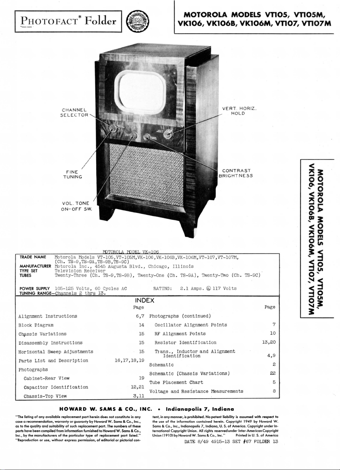
CHANNEL
SELECTOR
Fold
er
MOTOROLA MODELS VT1O5,
VK1O6,
VK1O6B,
VERT.
HOLD
CONTRAST
BRIGHTNESS
VK1O6M,
HORIZ.
VT1O7,
VT1O5M,
VT1O7M
28
oo
VOL.
TONE
ON-OFF
TRADE
NAME
Motorola
MANUFACTURER
TYPE
SET
TUBES
Twenty-Three (Ch.
POWER
SUPPLY
TUNING
RANGE—Channels 2 thru
Alignment
Block
Diagram
Chassis
(Ch.
Motorola
Television Receiver
105-125 Volts,
Instructions
Variations
SW.
Models
TS-9,T3-9A,TS-9B,TS-9C)
Inc.,
Disassembly Instructions
Horizontal Sweep Adjustments
Parts
List
and
Description
Photographs
Cabinet-Rear
Capacitor
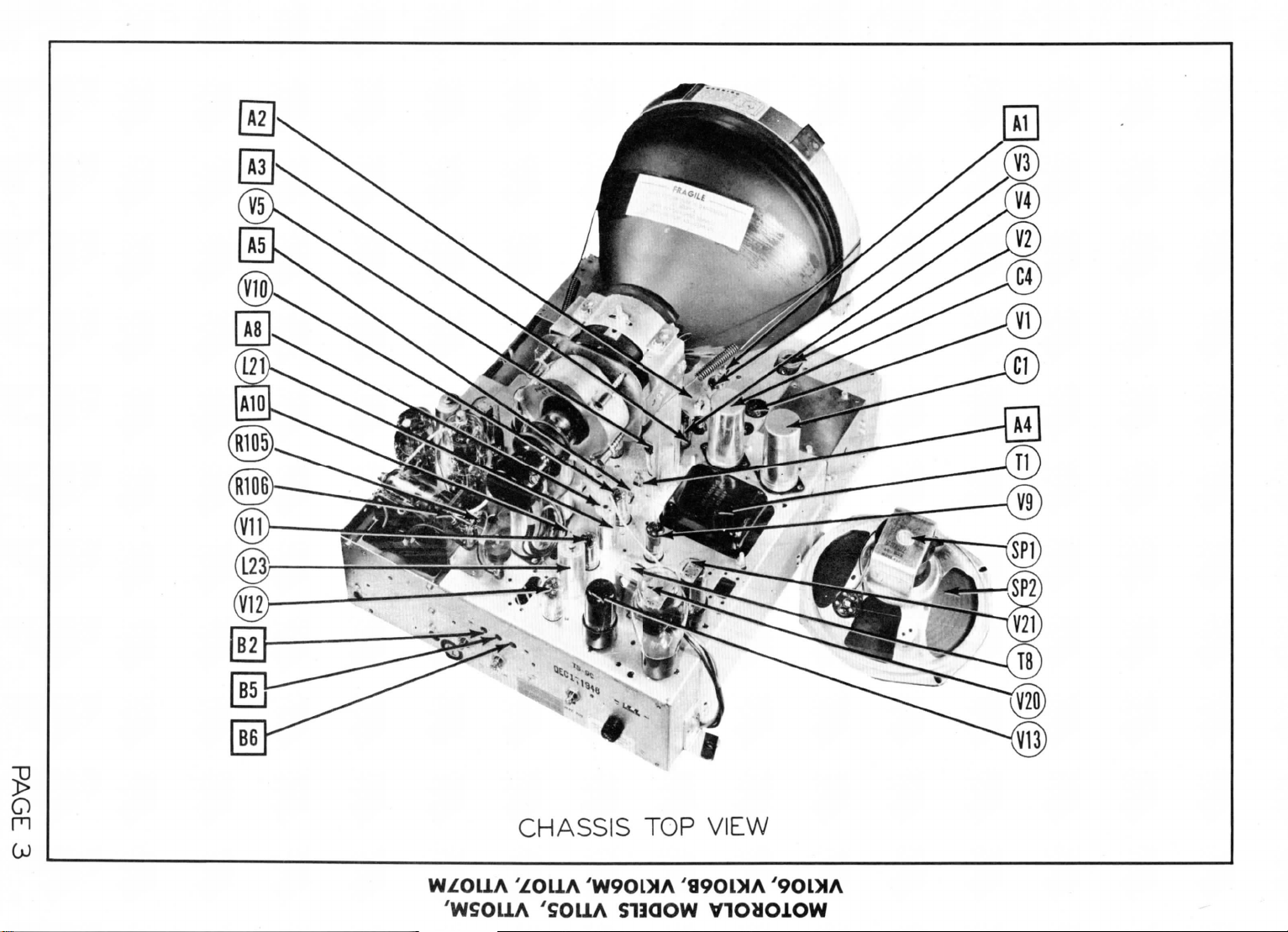
Chassis-Top
View
Identification
View
MOTOROLA
MODEL
VK-106
VT-105.VT-105M.VK-106,VK-106B.VK-106M,VT-107,VT-107M,
4545
Augusta
TS-9,TS-9B),
60
Cycles
15.
Blvd.,
AC
Chicago,
Twenty-One
RATING:
Illinois
(Ch.
2.1
TS-9A),
Amps.
Twenty-Two
<a>
117
Volts
INDEX
Page
6,7
Photographs (continued)
14
Oscillator Alignment Points
15
RF
Alignment Points
16
,17,18,19
12,21
3,11
Resistor
15
15
Trans.,
Schematic
Schematic
19
Tube Placement Chart
Voltage
Identification
Inductor
Identification
and
Alignment
(Chassis Variations)
and
Resistance Measurements
(Ch.
TS-9C)
Page
13,20
4,9
§>
?*
<
o
Ui
7
10
2
22
5
8
HOWARD
"The listing
of any
available
case a recommendation, warranty
as
to the
quality
have
by the
and
been compiled
manufacturers
or
parts
Inc.,
"Reproduction
suitability
from
of the
use, without
replacement
express
W.
part
guaranty
replacement
type
permission,
herein does
by
Howard
of
or
of
such
information furnished
particular
SAMS & CO., INC. • Indianapolis
not
constitute
W.
part.
The
to
Howard
replacement
of
editorial
Sams & Co.,
numbers
of
W.
Sams & Co.,
part
listed."
or
pictorial
in any
Inc.,
these
con-
tent,
in any
the
use of the
Sams & Co.,
ternational
Union
(1910)
manner,
is
prohibited.
information contained herein. Copyright
Inc., Indianapolis
Copyright Union.
by
Howard
W.
DATE
7,
Indiana
No
patent
liability
7,
Indiana,
rights
U. S. of
reservedunder
Inc."
All
Sams & Co.,
8/49 4915-13
is
assumed with
1949
America. Copyright under
Printed
SET
by
Inter-American Copyright
in U. S. of
#67
FOLDER
respect
Howard
America
W.
13
to
In-
Page 2
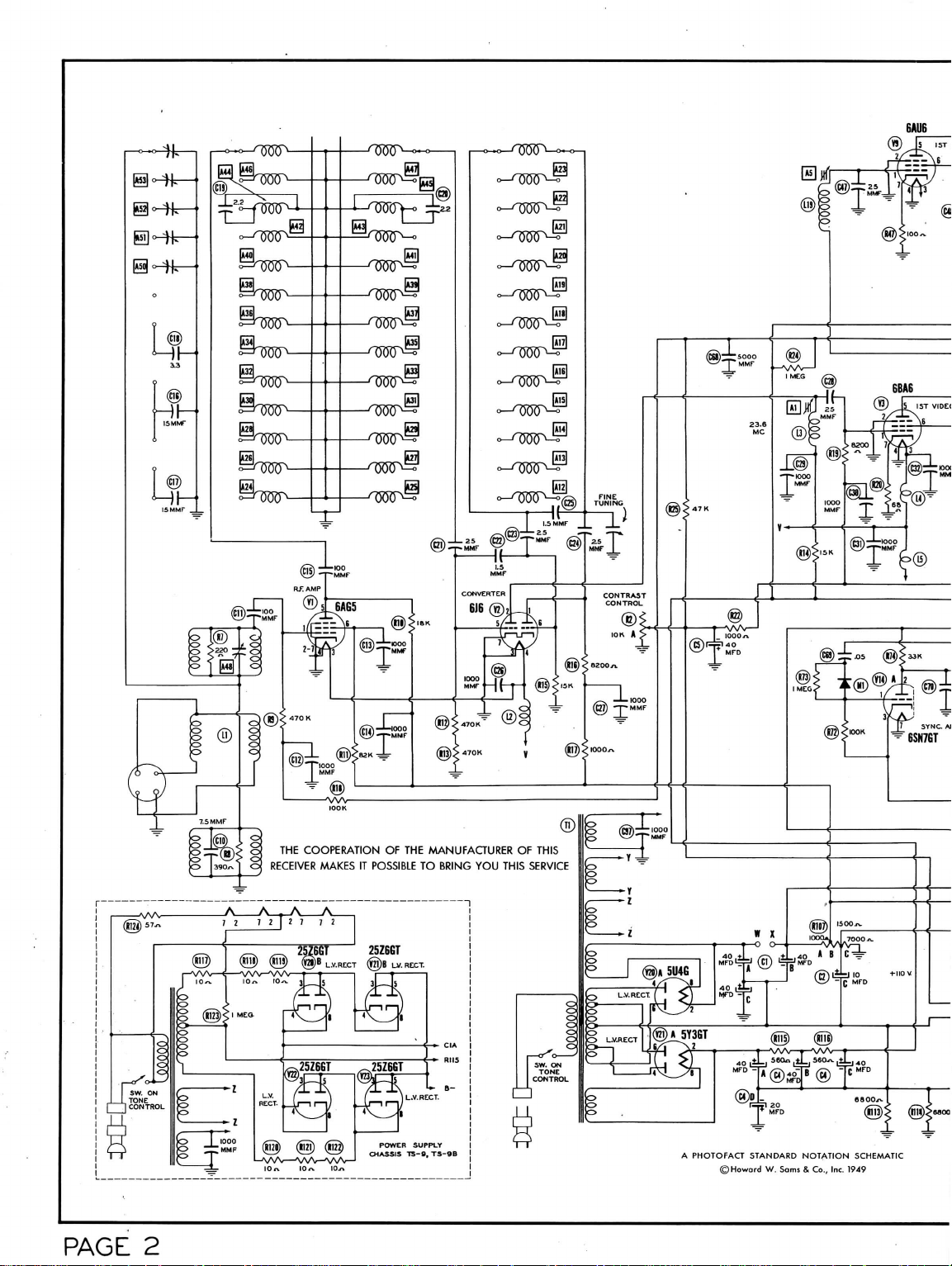
6AU6
PAGE
2
THE
COOPERATION
RECEIVER
MAKES
IT
POSSIBLE
OF THE
MANUFACTURER
TO
BRING
YOU
OF
THIS
THIS
SERVICE
A
PHOTOFACT
STANDARD
Howord
W.
Sams
NOTATION
8,
Co., Inc. 1949
SCHEMATIC
Page 3
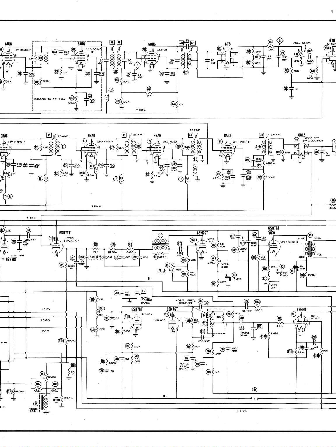
6AU6
CHASSIS
TS-9C
ONLY
r^J
(?*$>
I®
1001
Page 4
12AU7
12AU7
J
I
Page 5
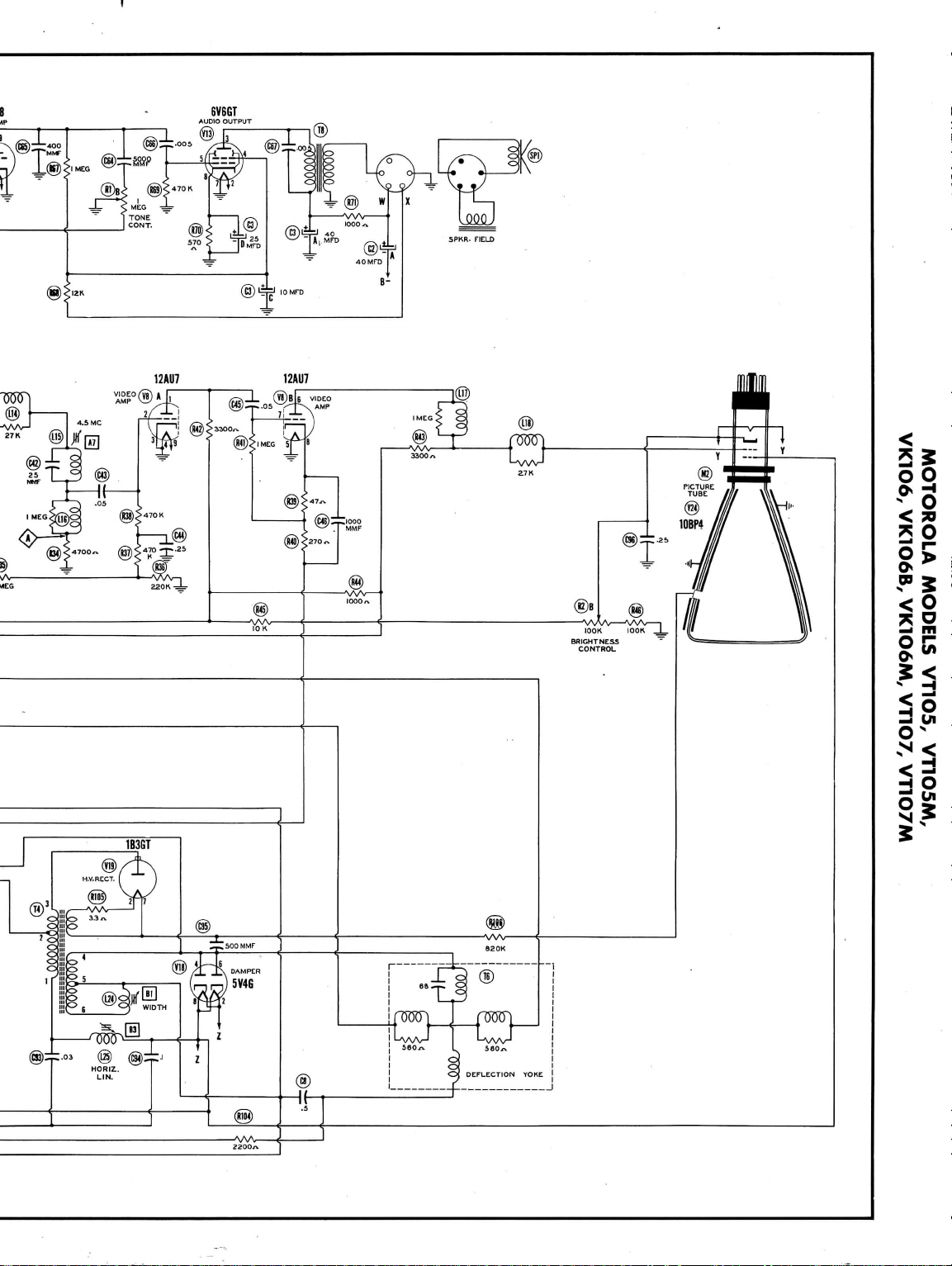
MOTOROLA
VK1O6, VK1O6B, VK1O6M, VT1O7,
MODELS
VT1O5,
VT1O5M,
VT1O7M
M3IA
dOl
SISSVHO
Page 6
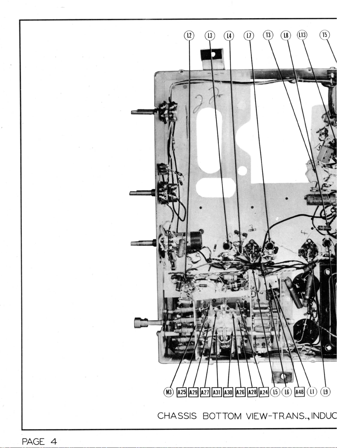
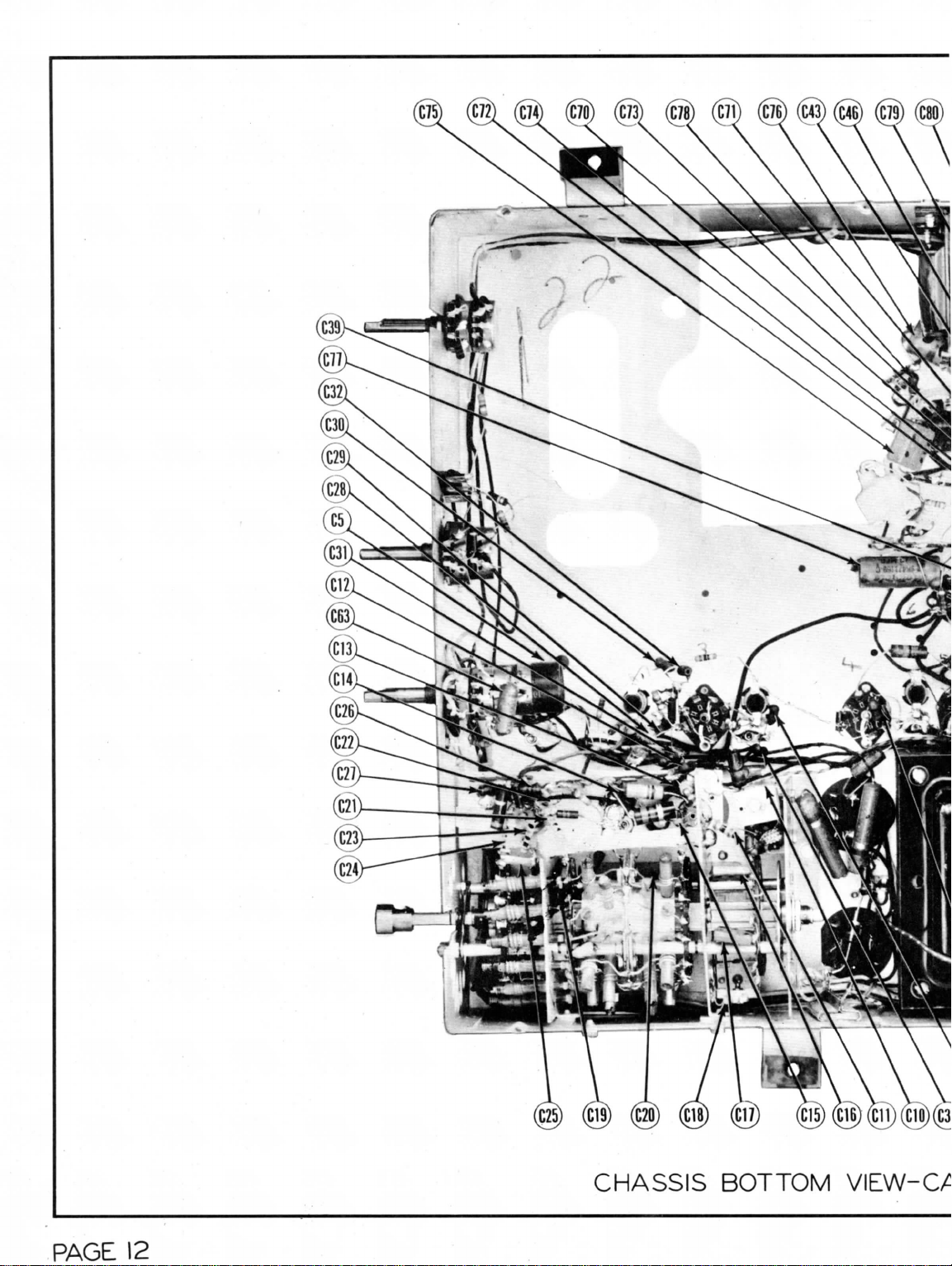
CHASSIS
BOTTOM
VIEW-TRANS.,
INDUC
PAGE
4
Page 7
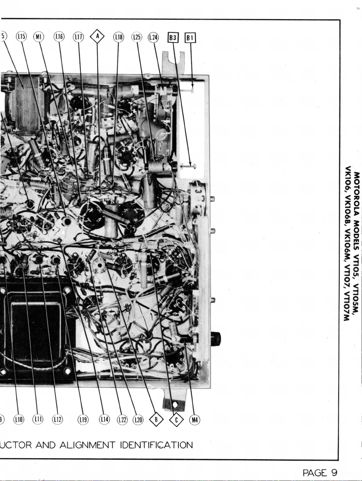
UCTOR
AND
ALIGNMENT
IDENTIFICATION
PAGE
9
Page 8
VERT
VERT.
OSC.
OUTPUT
SYNC.AMP/
SYNC
SEP.
V8
U2AU7
TUBE PLACEMENT CHART
PAGE
5
Page 9

Connect
positive
terminal
Set the
DUMMY
ANTENNA
High
.01MFD
(Grid)
Low
.01MFD
.01MFD
.01MFD
.01MFD
.01MFD
Connect
to
give
horizontal
DUMMY
ANTENNA
High
.01MFD
(Grid)
Low
There
.are
One
method
the
picture
adjustment
Another
RF
type
electronic
The
third
DUMMY
ANTENNA
High
.01MFD
of
side
Chassis
necessitate a change
DUMMY
ANTENNA
High
.01MFD
9.
10
11
12
the
minus
alignment.
has
adjustments
ANTENNA
See
13.
tlons
above
14.
(Grid)
Low
Detune
the
High
.01MFD
(Grid)
Low
.01MFD
Connect
generator should
the
Leave
Set the
The
enough
DUMMY
signal
the
antenna
Across
terminals
1002.
Instruc
n
ALIGNMENT INSTRUCTIONS
the
negative
contrast
SIGNAL
GENERATOR
COUPLING
side
of
side
the
synchronized
GENERATOR
COUPLING
side
of 6J6
side
three
Is
Is
eliminated
Is
being
method
method
GENERATOR
COUPLING
side
SALS
to
TS-9C
GENERATOR
COUPLING
side
of
side
discriminator transformer
side
of 6J6
side
the
signal
fine
contrast
adjustments
bandwidth
.
GENERATOR
COUPLING
antenna
terminal
to
chassis
control
to
pin
5
6J6
(V2).
to
chassis.
»
»
»
tl
tl
deflection.
SWEEP
to
pin
5
(V2).
to
chassis
possible
done
by
tuning
or
made.
Is
by
feeding a 4.
voltmeter across
of
using
SWEEP
to
pin
(V7).
chassis.
SIGNAL
7
Low
contains
to
6J6
to
to
to
n
generator
tuning
an
In
alignment procedure.
pin
5
(V2).
chassis
pin
5
(V2).
chassis
generator
be
connected
control
control
to
work
SIGNAL
.
»
of
ground.
to
give
SIGNAL
GENERATOR
FREQUENCY
23.6MC
26.4MC
22.9MC
25.7MC
21.9MC
24.7MC
sweep
voltage
SWEEP
GENERATOR
FREQUENCY
24MC
(10MC
Sweep)
methods
In a normal
minimized.
an
oscilloscope
SWEEP
GENERATOR
FREQUENCY
Off
additional
SIGNAL
GENERATOR
FREQUENCY
21.9MC
21.9MC
"
to the
Impedance.
set at the
for -3
on the
high
effectively over
SIGNAL
GENERATOR
FREQUENCY
215.75MC
209
.75MC
203.75MC
197.75MC
191.73MC
185.75MC
179.75MC
87.75MC
81.75MC
71.75MC
65.75MC
59.75MC
a -3
volt
-5
volt
bias.
CHANNEL
Any
»
"
n
"
«
from
MARKER
GENERATOR
FREQUENCY
21.9MC
26.4MC
4.
of
adjusting
picture
The
SMC
unmodulated
R41
(2nd
MARKER
GENERATO
FREQUENCY
4.
SMC
(400%
Mod.)
sound
CHANNEL
Any
secondary
Any
"
antenna terminals
through
1502.
For
Instance,
midpoint
volts
bias.
band
Is
CHANNEL
13
12
11
10
9
8
7
6
5
4
3
2
VIDEO
IF
(Measure
Probe
Common
C
ssis.
ALIGNMENT
to the
from
CONNECT
VTVM
to
to
battery
»
"
"
tt
n
OVERALL
the
SMC
fine
video
with a detector
IF
by
VIDEO
signal
generator
TMAMKIFI
CONNECT
CHANNEL
SCOPE
Any
Vert . Amp . to
Point<A>
to
TRAP ADJUSTMENT
this
trap.
and
adjusting
tuning
control
signal
amp.
grid
r-UiKiwei
CONNECT
CHANNEL
SCQpE
Any
Vert.
detector
pin 6
12AU7
IF
but the
CONNECT
VTVM
Probe
Common
turning
Probe
Common
ssis
side
ALIGNMENT
to
to
All out
to
to
.
SOUND
stage
DC
<J^
chassis.
€
"
RF
ALIGNMENT
The
(Measured
made
all
€
of the
high
side
If
the
of
its
from
at
195MC
these channels.
CONNECT
VTVM
Probe
to
Common
to
assis.
»
mixer
grid
center terminal
ADJUST
Point
Al
AS
A3
A4
AS
A6
IP
RESPONSE
to the
Low
trap
should
7 of
may be
Amp.
thru
probe
(plate)
(V8).
chassis.
side
A7 so the
SALS
Adjust
of
Low
chassis.
to
pin
circuit).
probe
to
transformer
ADJUST
Point
A8,A9
approximately 2 full
Point
A10
All
receiver through
should
arm of
channels
The low
be
Impedance
range during
control
ADJUST
A12
A13
A14
A15
A16
A17
A18
A19
A20
A21
A22
A23
generator
electrical
for
Point
at the
Junction
to
Adjust
n n n tt
n
n tl n n
Adjust
step
Adjust
CHECK
horizontal
ADJUST
be set on the
(V7)
A7 for
accomplished
ADJUST
A7
Adjust
to
added
Adjust
of R12 and
chassis.)
REMARKS
for
maximum
n tl n
for
minimum
4.
for
maximum
REMARKS
Check
Is
stippled
video
REMARKS
Is
fixed
for
maximum
deflection.
deflection. Repeat
deflection.
amplifier
similar
center audio peak
detector
minimum.
as
to see
to
or
half-tone
follows:
for
minimum
tuned
REMARKS
of the
that
and
and
deflection.
turns.
Adjust
for
maximum
Adjust
for
peak
correct
two
is
502,
zero
resistors.
negative
the
connected t hrough a resistor
the
to
chassis).
7,8,9,10,11,12
band
channels
Adjust
for
negative reading
side
zero reading. A positive
of the
deflection.
reading. A positive
Is
obtained
setting.
The low
the
resistor
oscillator
and 13.
have
correct
This
Individual antenna
REMARKS
will
setting.
n
R13.
Connect
oscilloscope
response curve
that
of Fig 1.
effect
while
connecting
amplitude.
does
on
either
of
1502
should
and RF
adjustment
be
obtained
not
side
be
of
on
the
In
this
an
and
side
and
either
of
PAGE
6
Page 10

15.
16.
17.
DUMMY
ANTENNA
11
SIGNAL
GENERATOR
COUPLING
n
ALIGNMENT
SIGNAL
GENERATOR
FREQUENCY
214MD
208MC
202M3
196MC
190ft
184
MC
178MC
86MC
80MC
70MC
64HC
58MC
195MC
86fC
80MC
70MC
64MC
58MC
CHANNEL
13
12
11
10
9
8
7
6
5
4
3
2
10
6
5
4
3
2
INSTRUCTIONS
CONNECT
VTVM
n
•
•
ADJUST
A24,
A25
A26.A27
A28.A29
A30,A31
A32.A33
A34.A35
A36.A37
A38.A39
A40,A41
A42.A43
A44.A45
A46,A47
MB
149
150
151
152
153
Adjust
CCONTJ
Unscrew
one
for
for
for
for
on
adjustment
maximum
slug
for
slug.
maximum
maximum
TS-9C.
maximum
Is
appreciably detuned.
slug
the
first
the
other
Adjust
Adjust
omitted
REMARKS
until
Adjust
deflection.
maximum.
deflection.
deflection.
deflection.
"
"
the
the
Then
Do not
A49
circuit
second
adjust
retune
Is
22
00
V3
<
70
5
o
FIG.
§>
I
Si
I!
en
OSCILLATOR
ALIGNMENT
POINTS
A13
^—™—
PAGE
7
Page 11

m
VOLTAGE
AND
RESISTANCE
MEASUREMENTS
oo
Itflm
V
1
6AG5
V2
6J6
V3
6BA6
V
4
6BA6
V5
6BA6
V
6
6AG5
V7
6AL5
V
8
12AU7
V9
6AU6
V
10
6AU6
V 1 1
6AU6
V
1 2
6T8
V
13
6V6GT
V
14
6SN7GT
V
15
6SN7GT
V16
6SN7GT
V17
6BG5G
V
18
5V40
V
19
1B30T
V20A
5U4G
V21A
5"I3GT
V24
4
Measured
§
Taken
«
Do not
Tub.
10BP4
with
measure.
-3.4VDO
150VDC
-20VDC
-20VDC
0V
0V
0V
0V
0V
-.5VDC
-.7VDC
0V
160VDC
from
vacuum
Pin
1
125VDC
»OV
4ov
4-.7VDC
43VDC
0V
0V
0V
pin
Pin
ov
87VDC
OV
OV
OV
1VDC
'-1.2VDC
-.5VDC
OV
OV
OV
-.8VDC
6. 3 VAC
460VDC
4360VDC
4133VDC
OV
390VDC
* DO NOT
325VDC
175VDC
93VDC
6 of
V15.
tube
voltmeter.
2
MEASURE
VOLTAGE READINGS
Pin
3
6.3VAC
OV
'
6.3VAC
6.3VAG
6.3VAC
6.3VAC
6
.3VAC
OV
6
.3VAG
6.3VAC
6
.3VAC
-9
.3VDC
270VDC
40V
410VDC
419.5VDC
417VDC
411VDC
43VDC
325VDC
OV
PIN
10
390V
DC
Pin
4
ov
6.3VAC
OV
OV
OV
OV
OV
OV
ov
ov -
OV
ov
270VDC
450VDC
4-28VDC
-41VDC
4320VDC
310VDC
380VAC
240VAC
PIN
11
160VDO
Pin
5
245VDC
-3.4VDC
118VDC
118VDC
118VDC
60VDC
OV
OV
110VDC
120VDC
50VDC
6
.3VAC
OV
I
225VDC
480VDC
4150VDC
4140VDC
4
.5VDC
43VDC
280VDC
OV
PIN
12
160VDC
Pin
6
245VDC
5-1VDC
118VDC
118VDC
118VDC
80VDC
60VDC
4155VDC
110VDC
120VDC
50VDC
-13VDC
300VDC
468VDC
40V
40V
4370VDC
310VDC
380VAC
240VAC
Pin
7
Pin
OV
ov
.1VDC
.1VDC
1VDC
1VDC
-.1VDC
*.5VDC
5VDC
1VDC
OV
OV
OV
OV
OV
OV
6. 3 VAC
57VACOV325VDC
45VDC
-.1VDC
6.3VAC
6.3VAC
6.3VAC
4270VDC
390VDC
187VDC
RESISTANCE
READINGS
Tub*
8
Pin?
6. 3 VAC
50VDC
TUP
(JAP
*
Item
V 1
6AG5
V
2
6J6
V
3
6BA6
V
4
6BA6
V5
6BA6
V6
6A05
V7
6AL5
V8
12AU7
V9
6AU6
V
10
6AU6
V 1 1
6AU6
V
12
6T8
V13
6V6GT
V14
6SN7GT
V
15
6SN7GT
V
16
6SN7GT
V17
6BG6G
V18
5V4G
V
19
1B3GT
V20A
5U40
V21A
5Y3GT
V24
10BP4
t
Measured
t
Measured
t
Measured
4
Measured
from
from
from
from
Pin
1
esoKffi
tlOKffi
10K2
F5KS2
.12
.22
Offi
I5.2K2
.12
10K2
100K2
100K2
Offi
4100K2
43.3Meg.
4750K2
4152
Inf.
Inf.
Inf.
Inf.
T15K2
pin
pin
pin
pin
Pin
2
Offi
tlSKffi
02
02
Offl
2002
2
Men.
1.2
Meg.
02
02
02
100K2
.12
T35KS2
T1.5K2
tSSKffl
02
#02
Inf.
10K2
24K2
I6.2K2
2 of V20
2 of V21
8 of
VIS
6 of V15
Pin
.12
•02
.12
.12
.Iffi
.12
'.12
02
.12
.12
.12
160K2
T1.2K2
40SZ
45.5K2
46002
4280K2
41002
4152
Inf.
lOKffi
Inf.
PIN
10
#02
3
Pin
4
02
.12
Offi
Offl
02
Offi
Offi
02
02
Offi
02
02
T12K2
2
Meg.
4
1 Meg
4200K2
18002
t95ffi
Inf.
480ffi
480ffi
PIN
11
(15K2
Pin
T20KS2
1
Meg.
tl.2Kffi
+1.2K2
41.2K2
411Kffi
02
02
42K2
410002
410K2
.12
470Kffi
T2K2
#3.8Meg.
#140K2
41
Meg.
4152
Inf.
lOKffi
Inf.
PIN
tlSKffi
5
12
Pin
teoKffi
13K2
41.2K2
41.2K2
41.2K2
46K2
411Kffi
T6.2K2
42K2
410002
410K2
47K2
T8502
47.5KB
402
402
T1102
T952
Inf.
4702
4602
6
Pin
7
Pin
8
Pin
9
Offi
Offi
682
682
682
2002
5K2
1.2
Meg.
3152
.12
1002
1002
02
10
Meg.
02
02
02
02
02
.Iffi
41
Inf.
4402
Inf.
Meg.
5002
.12
.12
.12
TlOKffi
#02
Inf.
10K2
24K2
T 1 Meg,
TUP
UAP
#2002
TUP
GAP
#3602
1.
DC
Voltage
ohms
ohms.
2. Pin
numbers
tion
3.
Measured
mon
per
volt;
on
bottom
negative
measurements
AC
Voltage
are
counted
of
socket.
values
are
unless otherwise
from
are at
measured
In a
clockwise
socket
stated.
pin to
20,000
at
1,000
direc-
com-
4.
Line
age
5.
Front
6.
Where
voltage
readings,
setting
and
maximum
panels
readings
of the
maintained
controls
may
service
controls,
readings
set at
vary
at
117
minimum.
according
ore
given.
volts
both
for
volt-
to the
minimum
Page 12

C
HASSIS
FRONT
PAGE
10
RF
ALIGNMENT
POINTS
Page 13

CHASSIS-TOP
VIEW
PAGE
11
Page 14
SISSVHO
39Vd
Page 15

$33)
v_y
(C34)
viy
(C35)
v_/
(C36)
vijx
(C37)
v_y
:APACITOR
IDENTIFICATION
PAGE
21
Page 16

R72)(R75)(R73)
PAGE
20
CHASSIS BOTTOM
VIEW-R
Page 17

MOTOROLA MODELS VT1O5,
VK1O6,
VK1O6B,
VK1O6M,
VT1O5M,
VT1O7,
VT1O7M
Q
6
Ld
Q
cr
O
CO
CO
LJ
cr
Page 18

m
R.F.AMP.
CONVERTER
1st
SOUND
2nd
SOUND
LIMITER
1st
VIDEO I.F.
2nd
VIDEO
3rd
VIDEO I.F.
4th
VIDEO
SYNC.
CLAMPER
SYNC.
AMP.
SYNC.
SEP.
I.
P. V 9
I.F.
V10
VI1
V3
I.F.
V4
V5
I.F.
V6
1/2 V 7
1/2 V14
1/2 V14
DISCRIMINATOR
VIDEO DET.
VERT.
1/2 V7
OSC 1/2
1/2
VI2
VI5
A.F.AMP.
AUDIO
VERT. OUTPUT
1/2 V12
OUTPUT
VI3
1/2
VI5
L.V.RECT.
L.V.RECT.
HOR.A.F.C.
1/2 V16
HOR.
BLOCK
OSC 1/2 V16
DIAGRAM
HOR.
OUTPUT
DAMPER
Page 19

BRIEF DESCRIPTION
CHASSIS
TS-9.
Twenty-two tubes plus
a
bridge
circuit
to
CHASSIS
TS-9A.
Same
as
TS-9 except a conventional power supply circuit
tubes.
The
power
transformer
10"
picture tube.
audio
to
TS-9A
except that
in
sound level with setting
CHASSIS
CHASSIS
TS-9B.
TS-9C.
tubes plus
Same
as
lifier
for
picture
Similar
variations
10"
picture tube.
TS-9 except that
tube.
to
OF
10"
picture
supply
the 1st
obtain greater audio
tube employing
"B"
power.
also
differs
Sound
an
additional Sound
CHASSIS
four
from
the one
IF
Amplifier
amplification.
of
IF
contrast control. Twenty-one tubes
VARIATIONS
type
25Z6GT
tubes operating
Is
used having
used
In
chassis TS-9. Twenty
Is
also used
Twenty
stage
was
two
added
as a
tubes plus
to
5Y3GT
and
reflex amp-
10"
reduce
plus
In
5U4G
HORIZONTAL
Adjust
the
horizontal oscillator
range
of the
horizontal hold control.
trimmer (B5) 2 1/E
whole range
and
will require tube
When
this
position.
Back
off
right;
then
Under these
zation.
HORIZONTAL
Turn
the
horizontal
for
best compromise between brightness
control (Bl) until
linearity
control (B3)
Due to
interaction between
to 3
turns from tight
of the
horizontal hold control.
and
circuit
has been
trimmer
turn
done,
B6
(Horizontal
the
horizontal hold control clockwise until picture "syncs"
conditions,
it
LINEARITY
size
control
the
picture fills
for the
turn the horizontal hold control to the extreme counter-clockwise
Bl and B2,
OSCILLATOR
coil
slug (B4)
If
this
or
component
frequency trimmer) until
should
be
possible
(Bl)
fully clockwise.
and
horizontal
the
mask
best horizontal linearity
adjustment
so the
cannot
until
it is
(If
this
checks.)
to
switch
AND
linearity.
horizontally
of one
picture
be
done,
possible
is
not
Vary
(8
on the
will
the
channels
SIZE
ADJUSTMENT
will
"lock-In" over
back*
off the
horizontal locking
to
sync
the
picture
possible,
the
plctue tends
without losing
receiver
to
ADJUSTMENT
the
horizontal drive trimmer (B2)
Adjust
the
horizontal size
1/2" minimum).
right half
require
Adjust
of the
readjustment
slip
in.
picture.
the
over
is
to the
synchroni-
the
of the
whole
the
defective
horizontal
other.
55
00
>*3
< 70
5
o
25
O
in
DISASSEMBLY
1.
Remove seven
2.
Remove screws holding back cover. Remove back cover.
3.
Remove
4.
Remove speaker plug from speaker.
5.
-Remove
6.
Remove four 5/16"
push-on
antenna
plug
four 7/16"
type
at
-chassis.
hex
head bolts holding
hex
nuts holding speaker. Remove speaker.
INSTRUCTIONS
MODEL
VK106
and one set
screw type control
chassis.
knobs.
Remove chassis.
PAGE
15
Page 20

ITEM
No.
*F
Amn
VI
•tro
"•
t
Vii
1st
V3
3nd
V4
VR
3rd
vD
4th
V6
Video
V7
Video
V8
1st
V9
2nd
VI
0
LImlter
Vll
Disc.-AF
V12
Audio
V13
3ync . Amp . —Sync
V14
Vert.
V15
Hor
V16
Hor . Output
V17
V18
Damper
HV
Rect.
V19
LV
Rect.
V20A
B
LV
Rect.'
LV
Rect.
V21A
B
LV
Rect.
LV
Rect.
V2S
LV
Rect.
V23
Picture
V24
ITEM
CAP.
No.
40
CIA
B
40
C
40
C"2A
40
10
B
C
10
D
250
C3A
40
15
B
C
10
25
B
C4A
40
B
40
C
40
D
20
05
40
C6A
40
B
10
25
C
C7
10
C8A
.5
.52
B
09
10
7.5
010
100
Oil
012
1000
1000
CIS
014
1000
015
100
C16
15
017
15
CIS
3.3
2
'2
C19
2
2
C20
C21
25
022
1.5
023
25
C34
25
C25
1.5
026
1000
027
1000
028
25
029
1000
030
1000
031
1000
032
1000
033
1000
1000
C34
C35
1000
036
1000
C37
1000
038
1000
039
1000
040
1000
041
10
C42
25
.05
043
C44A
.25
.1
B
045
.05
C46
1000
047
25
C48
1000
049
1000
C50
1000
C51A
1000
B
5000
USE
Video
Video
Video
Video
Det.-Sync.
Clamper
Amp.
Sound
Sound
Amp.
Output
Osc.
Output
AFC-Hor
Tube
RATING
VOLT
450
450
150
450
450
450
25
450
450
450
35
300
300
300
150
150
450
450
25
450
100
a
15,75
:ycle
450
500
500
100
400
400
400
MOTOROLA
PART
6AG5
6J6
IF
IF
IF
IF
IF
IF
6BA6
6BA6
6BA6
6AG5
6AL5
12AU7
6AU6
6AU6
6AU6
6T8
6V6GT
6SN7GT
Sep.
-Vert
6SN7GT
6SN7GT
Osc.
6BG6G
5V4G
1B3GT
5U4G
25Z6GT
5Y3GT
25Z6GT
25Z6GT
35Z60T
10BP4
Capacity values given
and
Paper Capacitors,
MOTOROLA
PART
No.
23A484197
23A484196
23A484195
4194
33A4E
33A485454
S3A4E
4195
33K4E
9031
33A485456
23K4E
9031
3104'
0735
0736
21X4r
31X4r
8410
31X478410
21X478410
31X470736
21R2736
31R2736
21K47
J.&J.U
21K4'~
j.oj.u
31A470738
de^i®
31X48
31A4-
07,38
21A4'
0738
31A470737
31K478410
31X478410
31K478410
31X47
8410
31X478410
31K478410
31K478410
21K478410
31K478410
21X478410
21K478410
21K478410
21X478410
21X478410
21A101778
21X28
816
8K471166
8K471167
21X478410
21X28816
21X478410
31X478410
21K478410
21K478410
21A470789
TUBES
REPLACEMENT
No.
AEROVOX
PART
No.
AFH88J8D
AFH822J50A
AFH832J5A
AFH888G4D
PRS150/40
PRS450/10
P288-5
PRS450/10
1468-0001
1468-001
1468-001
1468-001
1468-0001
1468-000025
1468-000025
1468-000025
1468-001
1468-001
1468-000025
1468-001
1468-001
1468-001
1468-001
1468-001
1468-001
1468-001
1468-001
1468-001
1468-001
1468-001
1468-001
1468-00001
1469-000025
P288-05
P488-25
P488-1
P488-05
1468-001
1469-000025
1468-001
1468-001
1468-001
1468-001
1467-005
(SYLVANIA
DATA
STANDARD
REPLACEMENT
6AG5
6J6
6BA6
6BA6
6BA6
6AG5
6AL5
12AU7
6AU6
6AU6
6AU6
6T8
6V6GT
6SN7GT
6SN7GT
6SN7GT
6BG6G
5V4G
1B3GT
5U4G
25Z6GT
5Y3GT
35Z6GT
S5Z6GT
25Z6GT
10BP4
CAPACITORS
in the
rating
and in
mmfd.
REPLACEMENT
CORNELL
PART
UP11CJ
UP9DJ
UP90DJ
UP9DJ
BR4015
UP9DJ
BR1045
GT2P5
BR1045
5W5T1
1W5D1
1W5D1
1W5D1
5W5T1
5W5Q25
5W5Q25
5W5Q25
1W5D1
1W5D1
5W5Q25
1W5D1
1W5D1
1W5D1
1W5D1
1W5D1
1W5D1
1W5D1
1W5D1
1W5D1
1W5D1
1W5D1
1W5D1
5W5Q1
5W5J25
GT2S5
GT4P25
GT4P1
GT4S5
1W5D1
5R5Q25
1W5D1
1W5D1
1W5D1
1W5D1
1D5D5
DUBILIER
No
1067
1068
1069
1070
1069
DATA
PART
GP1K-100
GP2L-001
GP2L-001
GP2L-001
GP1K-100
QP1K-25
NPOK-1 . 5
GP1K-25
GP1K-25
NPOK-1.
GP2L-001
GP2L-001
GP1K-25
GP2L-001
GP2L-001
GP2L-001
GP2L-001
GP2L-001
GP2L-001
GP2L-001
GP2L-001
GP2L-001
GP2L-001
GP3L-001
GP2L-001
GP1K-10
NPOL-25
GP2L-001
NPOL-25
GP2L-001
GP2L-001
GP2L-001
GP2L-001
GP2M-005
or
Equivalent)
RMA
BASE
TYPE
7BD
9BF
7BK
7BK
7BK
7BD
6BT
9A
7BK
7BK
7BK
9E
7AO
8BD
8BD
8BD
SET
5L
30
5t
7Q
5T
7Q
7Q
7Q
column
for
Mica
ERIE
No.
5
Used
in
Used
in
Used
in
Used
In
Used
In
Used
in
Used
in
are
in
and
Ceramic
SOLAR
PART
M-10-450
ST-2-5
M-10-450
MO.
5-31
MW.5-21
fW.5-21
MW.5-21
MO.
5-31
MO.
5-425
MO.
5-425
MO.
5-425
MW.5-21
MW.5-21
MO.
5-425
MW.5-31
MW.5-21
MW.5-21
MW.S-21
MW.5-21
MW.5-21
MW.5-21
MW.5-21
MW.5-21
MW.5-21
MW.5-21
MW.5-21
MO.
5-41
MOS.5-25
ST-4-05
ST-4-25
ST-4-1
ST-4-05
MW.5-21
MOS.5-42E
MW.5-21
MW.5-21
MW.5-21
MW.5-21
MW.5-25
chassis
chassis
chassis
chassis
chassis
chassis
chassis
mfd.
No.
NOTES
TS-9C
only.
TS-9A
and
TS-9
and
TS-9A
and
TS-9
and
TS-9
and
TS-9
and,TS-9B.
for
Electrolytic
Capacitors.
SPRAGUE
PART
PVL-54
rVL-40
TVA-9
FVL—
rVA-6
D6286
JT-401
FVL-40
TVA-6
PVA-21
rc-5
rVL-41
rVA-21
1FM-31
1FM-21
1FM-21
1FM-21
LFM-31
^S—
•B-415
•E-425
MS-425
1FM-21
1FM-21
MS-425
1FM-21
1FM-31
1FM-31
1FM-31
1FM-21
1FM-21
1FM-21
1FM-21
1FM-21
1FM-21
1FM-21
1FM-21
M3-41
MS-425
TM-15
TC-2
TM-1
PM-15
1FM-21
M3-425
1FM-21
1FM-21
1FM-21
1FM-21
1FM-25
IDENTIFICATION
No.
INSTALLATION
-
Filter
•
Filter
A
Filter
-
Filter
•
Filter
A
Filter
Vert.
40
415
Output
•
Vert.
A
Decoupling
Output
a
Filter
*
Filter
A
Filter
Filter
Bias
Filter
-
Filter
a
Decoupling
A
Output
Vert.
Output
Hor. Sweep
S. IF
Fixed
RF
Coupling
Bias
Filter
RF
Screen
RF
Bypass
RF
Coupling
;;
;; s
n II
RF
Coupling
Osc. Coupling
Osc.
Grid
Osc. Feedback
rixed
Trimmer
Filament Bypass
Osc.
Plate
IF
Coupling
Mixer
Plate
Bias
Filter
rilament
1st IF
1st IF
3ias
Filter
2nd
IF
3rd IF
3rd IF
4th IF
4th IF
4th IF
Diode
Filter
''ixed
Trimmer
Video
Coupling
Bias
Filter
" "
Video
Coupling
video Amp. Cath. Bypass
rixed
Trimmer
1st S. IF
S..
IF
Coupling
2nd
S.
2nd
S.
TS-90.
TS-9B.
TS-9C.
TS-9B.
TS-9B
.
CODES
AND
NOTES
Cath.
Output
Dec.
Oath.
Bypass
T
Cath.
Bypass
Decoup.
Coupling
Decoupling
Trimmer
t
Bypass
Cap.
Decoupling
5
Dec.
Bypass
Fll. Bypass
Decoupling
Decoupling
Fll. Bypass
Decoupling
Oath. Bypass
Decoupling
Plate
Decoup.
i
Decoupling
§
IF
Cath.
IF
Byp.
Decoupling
»
Byp.
T
t
§
**
*»
ITEM
No
052
053
054
055
056
C57
058
059
060
061
C62
C63
064
065A
C66
C67
068
069
070
071
072
073
074
C75
076
C77
078
079
C80
081
C82
C83
084
C85
C86
C87
088
089
C90
C91
C92
093
094
095
096
C97
ITEM
R1A
R2A
R3A
R4
R5
R6
ITEM
No.
R7
R8
R9
RIO
Rll
R12
R13
R14
R15
R16
R17
R18
R19
R21
R22
R23
R24
R25
R26
R27
R28
-129
R30
R31
R32
R33
R34
R35
R36
R37
B
No.
•Q
RATING
CAP
1000
5000
68
25
1000
25
250
5000
250
.1
5000
.01
5000
400
.002
.005
.005
5000
.05
120
250
.003
.005
.005
5000
.25
.1
1000
400
500
120
1000
.05
.02
.25
200
250
50C
2000
500
.1
400
500
.25
.05
600
7.5
.03
1000
.1
500
10000
.25
300
1000
*
Used
t
Used
•t
Not
§
Used
#
Used
f Not us
i
Used
**
Not
'RATING
RESIST-
ANCE
1
Meg.
1
Mep
10K2
100K2
1
Meg
30K2
2
Meg.
5K2
10002
RESISTANCE
2202
3902
470K2
18K2
82K2
470K2
470K2
15KS2
15K2
82002
10002
100K2
32002
22K2
10002
10002
1
Meg.
47K£
382
33K2
682
47002
2208
47002
47002
22KS2
4700S!
1.5
Meg.
220K2
470K2
VC
500
500
400
100
500
600
600
600
600
500
400
300
200
500
400
400
100
100
600
20C
600
only
c
used
c
o
o
used
.
RATING
IT
21K
21A
21K28816
21K478410
21K28816
21R
21A
8K4
21A
8K4
21A
21R
8K4
8K4
21A470789
8A4
21K484150
21R
31R6567
8K4
8K4
21K
21R6664
21X484150
21K.484150
21K478410
8K471166
8X471164
8A471356
21R6662
21R6568
21R6664
3A47
8X471167
210
8A471149
21A90013
8A471356
21K478410
in
nly in
in
nly in
nly in
ed
in
nly in
in
WATTS
i
~\
2
\t
2 J
±
_
!
2
J
4
WATTS
PARTS
MOTOROLA
PART
No.
4V473410
0789
2
66f
47C
)789
71]
69
47C
)789
71
63
47C
)789
66«
4
71]
62
71]
63
71]
51-A
2
666
84]
48
71]
69
47E
410
1356
t7C
735
models
m
Ddels
model
m
Ddel
m
3del
mo
iel
m
)del
model
mrvDAr
MO
PART
^
18A489005
1
18
A484072
18
A484073
}
18A484199
18A484800
18K780354
i
6R6270
T
6R6554
6R6377
2
6R476014
1
6R5575
6R6377
i
6R6377
X
6R2119
6R21
1
6R5610
6R6301
i
6R6031
6R2004
i
6R6007
6R6397
6R6301
5
6R6301
6R6004
6R6056
f
6R6007
I
6R6410
i
6R6007
f
6R6080
6R63933
I
6R6080
6R6080
6R6397
i
6R6080
6R3966
i
6R6407
6R6377
14£
14E
1468-00007^
1468-000025
1468-001
1468-00002^
146
146
146
P48
146
P48
146
146
P68
P68
P68
1467-005
P68
1468-0001
146
P68
P68
P68
1467-005
P48
P48
146
1468-0004
1468-001
P288-05
P488-02
P488-25
L468—
L467-002
P688-1
1468-0004
J488-25
P688-05
P1088-03
P688-1
P488-25
1468-001
TS-9A
TS-
TS-9C
TS-9
TS-9
TS-9
TS-9
TS-9B
REPLACEMENT
n
No.
REPLACEMENT
MOTOROLA
PART
K
19
LIST
AEROVOX
PART
No.
8-00
7-00
8-OOC
7-OOt
8-OOC
8-1
7-05
8-01
7-OOE
8-OOC
8-OOi
8-OQE
8-OOE
8-05
8-OOC
8-002
8-OOE
8-OOE
8-35
8-1
8-001
00025
and
9
an
C
B
PART
Qll-139
411-114
0.
Al
CAPACI"
REPLACEMEh
CORNELL-
DUB1LIER
PART
No.
1
IV
5D1
11
5D5
5W5Q25
1W5D1
5W5Q25
)25
5W
5T25
)
ID
5D1
)25
5W
5T25
GT
4PI
ID
5D5
GT
2S1
>
ID
5D5
)4
5W
5T4
GT
6D2
GT
6D5
GT
6D5
1D5D5
GT
6S5
SW5T1
25
5W
5T25
GT
6D2
GT
6D5
GT
6D5
1D5D5
GT
4S5
GT
4P1
1W
5D1
5W5T4
1W5D1
GT2S5
GT2S2
GT2P25
ci
icmoc:
OWOliiD
1W5D2
GT6P1
5W5T4
GT4P25
GT6R5
GT16S3
GT6P1
GT2P25
TS-9C
i
TS-9B
CO
v«vy
DATA
ID/"
No.
PAR
M-83M-1910-1C
RES
DATA
IRC
INO.
PART
BTS-470K
BTA-82K
BTS-470X
BTS-470K
BTS-1000
BT3-100K
BTS-8200
BTS-22K
BTS-1000
BTS-1000
BTS-1
Meg.
.BTS-47F
BTS-33K
BTS-4700
BTS-4700
BTS-4700
BTS-1.5Meg-5'
BTS-320K
BTS-470K
PAGE
16
Page 21

NOTES
sis
TS-9C
only.
sis
TS-9A
and
sis
TS-9
sis
TS-9A
sis
TS-9
sis
TS-9
sis
TS-9
r
Electrolytic
Capacitors.
1AOUE
CTNo
,-54
,-40
,-40
1-6
>gg
401
,-40
1—6
-5
,-41
L-21
1-31
1-21
1-21
1-21
1-31
415
-415
425
425
1-21
1-21
425
1-21
[-21
1-21
[-21
1-21
1-21
1-21
[-21
[-21
1-21
1-21
-21
41
425
15
2
1
15
-21
425
-21
-21
-21
-21
-25
TS-9C.
and
TS-9B.
and
TS-9C.
and
TS-9B.
and
TS-9B.
and
TS-9B.
IDENTIFICATION
INSTALLATION
Filter
Filter
Filter
Filter
•
Filter
*
Filter
Vert. Output Cath.
•
Filter
•
Vert. Output Dec.
A
Decoupling
Output
Cath.
a
Filter
*
Filter
A
Filter
filter
31as
Filter
•
Filter
T
•
Decoupling
*
Output Cath.
Vert.
Output Decoup.
Hor.
Sweep
S. IF
Decoupling
rixed
Trimmer
^F
Coupling
Bias
Filter
HF
Screen Bypass
rtF
Bypass
RF
Coupling
b
Ixed
Trimmer
1
!!
ii
ti
RF
Coupling
Osc. Coupling
Osc. Grid Cap.
Dsc.
Feedback
rlxed
Trimmer
i1 i lament
Bypass
Osc. Plate Decoupling
IF
Coupling
Mixer
Plate
31as
Filter
i"llament
Bypass
1st
IF
Fll.
1st
IF
Decoupling
Bias
Filter
2nd IF
Decoupling
3rd IF
Fll.
3rd IF
Decoupling
4th IF
Cath. Bypass
4th IF
Decoupling
4th IF
Plate Decoup.
Diode
Filter
Fixed
Trimmer
Video
Coupling
Bias
Filter
n
,i
t
Video
Coupling
video
Amp. Cath. Bypass
rixed
Trimmer
1st S. IF
S..
IF
Coupling
2nd
S. IF
2nd S. IF
"
" "
PARTS
RATING
ITEM
CAP.
No.
C52
1000
CSS
5000
68
054
C55
25
056
1000
C57
25
250
C58
C59
5000
C60
250
.1
C61
C62
5000
C63
.01
C64
5000
C65A
400
.002
B
C66
.005
C67
.005
C68
5000
C69
.05
120
C70
C71
250
.002
072
073
.005
C74
.005
C75
5000
C76
.25
C77
.1
078
1000
079
400
080
120
C81
120
082
1000
CBS
.05
.02
C84
085
.25
086
250
087
CODES
AND
NOTES
*
Byp.
Bypass
Bypass
Coupling
T
§
*
#
«
RESISTORS
§
Dec.
Bypass
Bypass
Decoupling
Cath.
Decoupling
* •
5
Byp.
§
»*
»«
2000
C88
.1
C89
400
25
C90
091
!os
C92
7.5
C93
.03
.1
C94
500
095
C96
.25
097
1000
*
Used only
T
Used only
4-
Not
§
Used only
»
Used
t Not us
i
Used
*» Not
ITEM
No.
R1A
R2A
R3A
R4
R5
R6
ITEM
No.
R7
R8
R9
RIO
Rll
R12
R13
R14
R15
R16
R17
R18
R19
R20
R21
R22
R23
R24
R25
R26
R27
R28
R29
R30
R31
R32
R33
R34
R35
R36
R37
B
B
B
2202
3902
470K2
18K2
82K2
470K2
470K2
ISKffl
15K2
82002
10002
100K2
82002
682
22K2
10002
10002
1
47K2
682
33K2
682
47002
2202
47002
47002
22KB
47002
1.5
220K2
470K2
RESIST-
ANCE
1
Meg.
1
Meg.
10K2
100K2
1
Meg.
30K2
2
Meg.
5KS!
10002
RESISTANCE
Meg.
Meg.
•1
VOLT
50C
500
400
100
500
600
600
600
600
500
400
200
200
500
400
400
500
100
100
200
iOC
500
600
500
600
100
3
600
10000
200
used
o
o
used
RATING
RATING
21K
2L4
21K
21K
21K28816
21R6662
21A
8K4
21A
8K4
21A
21R6664
8K4
8K4
21A
8A4
21K484150
21R6662
21R
8K4
8K4
21K
21R
21K
2
21K478410
8K471166
8K471164
8A471356
21R6662
21R6568
21R6664
8A471356
8K471167
21C
8A471149
2U9001S
8A471356
21K478410
in
In
In
In
nly
in
ed in
nly in
In
WATTS
i
"}
j
}
4
^
WATTS
i
2
x
H
X
I
£
I
X
£
i
•£
£
1
i
X
i
I
MOTOROLA
PART
No.
478410
470789
28816
478410
470789
71169
470789
71163
470789
71162
71162
470789
71151-A
S567
84148
71169
478410
5664
484150
IK
170735
models
models
model
model
model
model TS-9
model
model
MOTOROLA
PART
18A489005
18A484072
13A484073
18A484199
18A484800
18K780354
i
6R6270
6R6554
6R6377
6R476014
1
6R5575
6R6377
6R6377
i
6R2119
6R2119
1
6R5610
6R6301
6R6031
6R2004
6R6007
6R6397
6R6301
£
6R6301
X
6R6004
£
6R6056
6R6007
6R6410
6R6007
6R6080
6R63933
1
6R6080
6R6080
6R6397
6R6080
6R3966
i
6R6407
i
6R6377
MOTOROLA
AEROVOX
146
146
14E
14
146
1468-000025
1468-00025
146
146
P48
146
P48
146
1468-0004
P68
P68
P68
146
pea
1468-0001
1468-00025
P68
P68
P68
146
P48
P48
146
146
1468-001
P288-05
P488-02
P488-25
1468—00025
1467-002
P68
1468-0004
^488—
P688-05
P10
P688-1
P488-25
1468-001
TS-9A
TS-9
TS-9C
TS-9C
TS-9
TS-9
TS-9B
RE
No.
REP
PART
K
LIST
PART
No.
8-00
7-00
8-00
£
8-00
8-00
7-OOE
8-OOC
8-1
7-05
8-01
7-OOE
8-002
8-OQE
8-OOE
7-OOE
8-05
8-002
8-OOE
8-OOE
7-OOE
8-25
8-1
8-001
8-OOC
3-1
25
38-03
and
and
B
'LACE
PART
yn-139
Qll-
ACEW
0.
AND
CAPACITORS
REPLACEMEN'
CORNELL
DUBILIER
PART
1
1W
5D1
3
IE
5D5
3075
5W
5*7
3026
5W
5Q25
L
1W
5D1
5W5Q25
5W5T25
ID
5D1
25
5W
5T25
GT
4PI
ID
5D5
GT
281
ID
5D5
5W5T4
GT
DD2
GT
5D5
GT
5D5
ID
5D5
GT
5S5
5W5T1
5W5T25
GT
5D2
GT
5D5
GT
5D5
ID
5D5
GT
4S5
GT
1P1
5D1
1U
4
5S.
5T4
1W5D1
GT2S5
GT2S2
GT2P25
5W5T25
1W5D2
GT
3P1
5W5T4
GT4P25
GT6S5
GT
16S3
GT6P1
GT2P25
TS-9C
TS-9B
v*ENT
DA
TA
IRC
No.
M-83-S
114
M-19-S
;NT
OAI
A
IRC
PART
BTS-47
OK
BTA-82
K
BTS-47
OK
BTS-47
OK
BTS-1000
BT3-10
OK
BTS-82
00
BTS-22
K
BTS-10
00
BTS-1000
BTS-1
Meg.
BTS-47
K
K
BTS-33
BTS-4700
BTS-47
00
BTS-47
00
BTS-1.5Meg-5%
BTS-22
OK
BTS-470K
DESCRIPTIONS
CCONTO
DATA
ERIE
PART
No
(
JP2L-
JP2I1-
C
C
iPlK-
C
iPlK-
c
,P2L-
GP1K-25
GP2K-250
C
P2M-
G
P2KT
C
P2M-
C
P2-3.
P2M-
C
GP2K-500
G
P2M-
G
P2M-
C
P2M-
G
P2M-
GP1K-100
GP2K-250
G
P2M-
G
P2M-
G
P2M-
G
P2M-
G
P2L-
GP2L-001
CONTROLS
CLAROSTAT
PART
No.
0
10-100
INO.
ALL
Ant.
RF
G
RF
P
RF
S
Mixe
Mixer
Osc.
Osc.
Osc.
Bias
1st
1st
1st
Bias
"
"
"
2nd
2nd
3rd
3rd
4th
4th
Video
4th
4th
Vide
Voltage Divider
"
Bias
SOLAR
No.
PART
001
MW.5-21
005
I*.
75
MOS.5-47
25
MO.
001
rW.5-21
MO.
MO.
305
MW.5-25
250
MS'.
ST-4-1
005
MW.5-25
35-01
ST-4-01
005
MW.5-25
MO.
302
ST-6-002
305
ST-6-005
305
ST-6-005
305
KW.5-25
ST-6-05
MO.
MW.
302
ST-6-002
305
ST-6-OOS
305
ST-6-005
305
MW.5-25
ST-4-25
ST-4-1
301
MW.5-21
MO.
MW.5-21
ST-4-05
ST-4-02
ST-2-25
MO . 5-325
MJ.5-22
ST-6-1
10 . 5-34
ST-2-25
ST-6-05
STM-16-OS
ST-6-1
ST-2-85
MW.5-21
Tonemcon?rol°and
B?i£htness°Mntrol
Vertical
hold control
Horizontal hold
Vertical size
Vertical linearity control
Focus control
REISTORS
ARE - 10%
Coil
Shunt
rid
late
creen
r
Grid
Plate
Decoupling
Grid
20%
Plate
Plate Decoupling
Network
See
Video
IF
Grid
Video
IF
Cathode
Video
IF
Transformer
Network
n
"
See
it
ii
Video
IF
Cathode
Video
IF
Transformer
Video
IF
Cathode
ifldeo
IF
Transformer
Video
IF
Cathode
IF
Plate Decoupling
i/ideo
IF
Decoupling
Video
IF
Transformer
o
Det. Load
"
Filter
SPRAGUE
PART
No.
1
5-25
IF
IFI
5-425
MS-4--.5
1FM-/.:.
5-425
M3-4fc-V.
5-325
IFM-S;;S
1FM-26
5-325
IFM-325
FM-1
1FM-21
PM-11
1FM-25
5-34
1FM-34
TM-22
FM-25
TM-25
1FM-25
m-15
5-31
IFM-31
5-325
IFM-325
IM-22
TM-25
TM-25
IFM-25
rc-2
PM-1
IFM-21
5-34
1FM-34
IFM-21
I'MIT1-12
'C-2
1
FTl-325
1FM-22
TM-1
1FM-34
TC-2
TM-15
TR-13
TM-1
TC-2
IFM-21
INSTALLATION
cont.rol
IDENTIFICATION
No.
(.'f*l-21
S. IF
',-25
Audio
Limiter
i-475
Sound
Llmlter
RF
De-emphasis
Audio
RF
Bias Filter
Audio
Tone
AF
n
it
Audio
Output Plate Bypass
Bias Filter
Sync.
Sync.
Sync.
Integrator Net.
Vert.
Vert.
Vert. Discharge
Sync.
Voltage
Ior.
15
Hor.
AFC
lor.
tor.
Ior,
lor.
ior.
Hor. Output Screen Byp.
AFC
Damper Filter
Damper Filter
CV
3lc.
Filament
switch)
>
_ ' ,,„,,„„„<-,,<,.
control
>
^
CODES
UNLESS
AND
INSTALLATION
Screen Bypass
Coupling
IF
Bypass
Coupling
Bypass
Coupling
Comp.
Plate
Coupling
Coupling
Amp. Plate Bypass
Coupling
ii
Oec.
Coupling
Sep. Cath. Byp.
Sync. Coupling
AFC
Filter
Osc. Grid Cap.
Discharge
Osc.
Coupling
Output Cath. Byp.
IF
Grid
Coupling
Decoupling
•
•
Bypass
tr
A
f
ii
Grid
Divider
Plate
Plate
NOTES
•
Bypass
Feedback
Filter
Tube Cath.
Bypass
NOTES
Dual
Concentric
Dual
Concentric
Dual
Concentric
OTHERWISE
STATED.
20%
Note
1
20%
Shunt
Note
1 20%
n
ii
20%
Shunt
Shunt
20%
See
Note
Shunt
'
5%
2
»
t
A
t
#
Cap.
Decoup.
Dec.
ITEM
R38
R39
R40
R41
R42
R43
R44
R45
R46
R47
R48
R49
R50
R51
,
R52
R53
R54
R55
R56
R57
R58
R59
R60
R61
R62
R63
R64
R65
R66
R67
R68
R69
R70
R71
R72
R73
R74
R75
R76
R77
R78
R79
R80
R81
R82
R83
R84
R85
R86
R87
R88
R89
R90
R91
R92
R93
R94
R95
R96
R97
R98
R99
R100
R101
R102
R103
R104
R105
R106
U07A
R108
R109
R110
Rill
R112
R113
R114
R115
R116
R117
R118
R119
R120
R121
R122
R123
R124
No.
RESISTANCE
470K2
472
2702
1
Meg.
33002
33002
10002
10K2
100K2
1002
10002
1002
10K2
39002
100K2
56002
100K2
iooa
15K2
10K2
470K2
10
150K2
100K2
100K2
100K2
47K2
33K2
10
1
Meg.
12K2
470K2
2702
10002
100K2
1
Meg.
33K2
68002
22K2
82002
68002
470K2
1
Meg.
3.3
1.5
220K2
5602
3.3
10002
33002
56K2
33K2
560K2
8200S
180K2
100K2
100K2
3.3
150KS2
120K2
10K2
472
1
Meg.
822
10K2
560K2
22002
3.32
820K2
10002
B
15002
C
70002
22002
18002
10002
270ffl
5602
68002
68002
5602
5602
102
102
102
102
102
102
1
Meg.
572
Meg.
Meg.
Meg.
Meg.
Meg.
Meg
Note
Note
Note
Note
Note
Note
Note
Note
Note
Note
Note
Note
Note
Note
Note
Note
Note
Note
RATING
WATTS
.
1. Not
2.
Chassis
3.
Chassis
4.
Chassis
5.
Used
6.
Used
7.
Chassis
8.
Chassis
9.
Chassis
10.
Chassis
11.
Chassis
12.
Chassis
13.
Chassis
14.
Chassis
15.
Ussd
16.
Chassis
17.
Used
18. Two
4
i
I
?
i
2
1
•^
^
i
^
^
£
^
Jj
Jj
i
^
i
1
i
•^
i
i
i
^
i
i
4
^
1
2
2
i
2
i
j
JT
i
i
1
i
i
i
JT
i
i
i
l
i
|
2
i
1
4
i
25
i
2
10
1
2
£
2
2
2
2
2
2
2
2
i
10
used
In
In
In
In
5602
REPL
MOTOROl
PART
6R6377
6R2108
6R6004
6R5581
6R2029
6R6327
6R6320
6R6031
6R6018
6R6301
6R6018
6R6320
6R6031
6R6031
6R6018
6R2119
6R476060
6R6377
6R6398
6R6031
6R6031
6R6031
6R6410
6R2109
6R6004
6R6430
6R6377
6R488036
6R476004
6R6031
6R6004
6R6400
6R6428
6R6397
6R2004
6R6428
6R6377
6R6004
6R2118
6R3966
6R6407
6R6291
6R2118
6R476004
6R5581
6R6378
6A489166
6R5697
6R2004
6R6444
6R6031
6R6031
6R2118
6R6398
6R5698
6R6320
6R2108
6R6004
6R488113
6R476060
6R5697
17K48541.
6R2053
17A48541
6R3964
6R488036
6R488036
6R488036
6R488144
6R488144
6R488144
6R488144
6R488144
6R488144
6R6004
17A4348L
in
oh
TS-9
TS-9
TS-9
chassi
chassi
TS-9
TS-9B
TS-9
TS-9
TS-9,
TS-9A
TS-9
TS-9
some
TS-9
chassi
1W re
c
N
u
u
u
u
u
u
u
u
a
Page 22

•SCRIPTIONS
)NTO
SOLAR
SPRAGUE
PART
No.
PART
MW.5-21
MW.5-25
MOS.5-47
MO.
MW.5-21
MO.
MO.
MW.5-25
!•£>'.
ST-4-1
MW.5-25
ST-4-01
MW.5-25
MO.
ST-6-002
ST-6-005
ST-6-005
I*.
ST-G-05
MO.
MW.
ST-6-002
ST-6-005
ST-6-005
MW.5-25
ST-4-25
ST-4-1
MW.5-21
MO.
MW.5-21
ST-4-05
ST-4-02
ST-2-25
MO.
MW.5-22
ST-6-1
MO.
ST-2-25
ST-6-05
STM-16-0;
ST-6-1
ST-2-25
MW.5-21
ue
control
control
rast
itness
leal
sontal
cal
leal
3
control
ORS
Shunt
i(."-]_£l
lF:;-25
IF!
5-425
MS-4',5
1FM-2!
5-425
M3-4t-:
IFM-S;:S
5-325
1FM-26.
5-325
IFM-325
LFM-21
ra-u
IF
M-25
5-34
1FM-34
^M-22
"M-25
TM-25
5-25
1FM-25
'M-15
5-31
1FH-31
5-325
IFM-325
TM-22
FM-25
'M-25
1FM-25
FC-2
TM-1
FM-21
5-34
1FM-34
1FM-21
TM-15
TM-12
TO
-2
5-325
IFM-325
1FM-22
TM-1
5-34
If
M-34
TC-2
'M-15
TR-13
TM-1
'C-2
FM-21
INSTALLATION
\ , p..-,..,-..,,,.,
and
switch)
control
-.
control
hold
control
hold
control
size
control
linearity
IDENTIFICATION
ARE - 10%
"
a
te
Decoupling
e
e
Decoupling
ork
See
Note
IF
IF
IF
Transformer Shunt
ork
IF
Cathode
IF
Transformer Shunt
IF
Cathode
IF
Transformer Shunt
IF
Cathode
IF
Plate Decoupling
IF
Decoupling
IF
Transformer Shunt
.
Load
Ivider
1
Grid
Cathode
Z<3b
See
Note 1 20%
n
M
n
20%
20%
5%
IDENTIFICATION
No
INSTALLATION
S.
IF
Screen
Audio
1-475
J
control
UNLESS
20%
See
Coupling
Limiter
Sound
IF
Limiter
RF
Bypass
De-emphasis
Audio
Coupling
^F
Bypass
Bias
Filter
Audio
Coupling
Tone
Comp.
AF
Plate
Audio
Coupling
Output
Plate Bypass
Bias Filter
Sync.
Cou'jllng
Sync.
Amp. Plate Bypass
Sync. Coupling
Integrator Net.
ii
ti
Vert.
Osc.
Vert. Coupling
Vert.
Discharge
Sync. Sep. Cath. Byp.
Voltage
Divider
Ior.
Sync.
Hor.
AFC
AFC
Filter
n
ii
ior.
Osc.
Ior.
Discharge
Hor. Osc. Plate Decoup.
Hor. Coupling
lor.
Output
Hor. Output Screen Byp.
AFC
Feedback
Damper Filter
Damper
Filter
IV
Filter
3ic.
Tube Cath. Dec.
Filament
NOTES
Dual
Dual
„
',
>
Dual
^
CODES
OTHERWISE
Note
2
CODES
AND
NOTES
Bypass
IF
Grid
if
Coupling
Decoupling
»
i
*
Bypass
#
I
#
Grid
Cap.
Coupling
Plate Bypass
Grid
Cap.
Cath.
Byp.
Bypass
c™<=e.,trlc
concentric
(._.,„._,....,,
Loneentrlc
STATED.
A
•
20%
R38
R39
R40
R41
R42
R43
R44
R45
R46
R47
R48
R49
R50
R51
.
R52
R53
R54
R55
R56
R57
R58
R59
R60
R61
R62
R63
R64
R65
R66
R67
R68
R69
R70
R71
R72
R73
R74
R75
R76
R77
R78
R79
R80
RSI
R82
R83
R84
R85
R86
R87
R88
R89
R90
R91
R92
R93
R94
R95
R96
R97
R98
R99
R100
R101
R102
R103
R104
R105
R106
U07A
R108
R109
R110
Rill
R112
R113
R114
R115
R116
R117
R118
R119
R120
R121
R122
R123
R124
ITEM
No.
RESISTANCE
470K2
472
2702
1
Meg.
33002
33002
10002
10K2
100K2
1002
10002
1002
10K2
3900S2
100K2
56002
100K2
1002
15K2
10K2
470K2
10
150KS2
100K2
100K2
100K2
47K2
33K2
10
1
Meg.
12K2
470K2
2702
10002
100K2
1
Meg.
33K2
68002
22K2
82002
68002
470K2
1
Meg.
3.3
1.5
220K2
5602
3.3
10002
33002
56K2
33K2
560K2
82002
180K2
100K2
100K2
3.3
150K2
120K2
10K2
472
1
Meg.
822
10K2
560K2
22002
3.32
820KS2
10002
B
15002
C
70002
22002
18002
10002
2702
5602
68002
68002
5602
5602
102
102
102
102
102
102
1
Meg.
572
RATING
WATTS
4
i
1
4
2
1
4
4
4
4
4
4
4
4
4
i
Meg.
Meg.
Meg.
Meg.
Meg
Meg
J
4
4
4
\
2
2
4
4
2
4
i
4
i
i
\
4
4
4
.
4
i
4
4
4
4
4
^
£
.
4
1
£
2
2
4
1
4
i
25
4
2
10
1
2
2
2
2
2
2
2
2
2
2
2
'
Note
Note
Note
Note
Note
Note
Note
Note
Note
Note
Note
Note
Note
Note
Note
Note
Note
Note
4
10
1. Not
2.
Chassis TS-9 uses 10K2 resistor
3.
Chassis TS-9 uses
4.
Chassis TS-9 uses
5.
Used
6.
Used
7.
Chassis
8.
Chassis
9.
Chassis TS-9 uses
10.
Chassis TS-9
11.
Chassis TS-9,
12.
Chassis
13.
Chassis TS-9 uses
14.
Chassis TS-9 uses
15.
Used
16.
Chassis TS-9
17.
Used
18. Two
REPLACEMENT
MOTOROLA
PART
No.
6R6377
6R2108
6R6004
6R5581
6R2029
6R6327
6R6320
6R6031
6R6018
6R6301
6R6018
6R6320
6R6031
6R6031
6R6018
6R2119
6R476060
6R6377
6R6398
6R6031
6R6031
6R6031
6R6410
6R2109
6R6004
6R6430
6R6377
6R488036
6R476004
6R6031
6R6004
6R6400
6R6428
6R6397
6R2004
6R6428
6R6377
6R6004
6R2118
6R3966
6R6407
6R6291
RR P 1 1
P
DntillO
6R476004
6R5581
6R6378
6A489166
6R5697
6R2004
6R6444
6R6031
6R6031
6R2118
6R6398
6R5698
6R6320
6R2108
6R6004
6R488113
6R476060
6R5697
17K485412
6R2053
17A485413
6R3964
6R488036
6R488036
6R488036
6R488144
6R488144
6R488144
6R488144
6R488144
6R488144
6R6004
17A484810
used
In
chassis
In
chassis
In
chassis
TS-9 uses 2 47KS2
TS-9B
uses
uses
TS-9A
TS-9A
and
in
some chassis
and
in
chassis TS-9
5608
1W
resistors
RESISTORS
DATA
PART
BTS-470K
BTS-1 Meg.
BTS-3300
BT-2-3300
BTA-1000
BTS-10K
BTS-100K
BTS-1000
BTS-3900
BTS-100K
BTS-5600
BTS-15K
BTA-10K
BTS-470K
BTS-10
BTS-150K
BTS-100K
BTS-100K
BTS-100K
BTS-47K
BTS-33K
BTS-10
BTS-1 Meg.
BTA-12K
BTS-470K
2-BT-2-560
BT-2-1000
BTS-100K
BTS-1 Meg.
BT-2-33K
BTS-6800
BTS-22K
BTS-8200
BTS-6800
BTS-470K
BTS-1 Meg.
BTS-3.3
BTS-1. 5 Meg.
BTS-220K
BTS-560
BTS—
BTA-1000
BTS-3300
BTS-56K
BTS-560K
BTS-8200
BTS-180K
BTS-100K
BTS-100K
BTS-150K
BTA-120K
BTS-10K
BTS-1 Meg.
BT-2-10K
BTS-560K
BTS-2200
BW-4-3.3
AB-1000
AB
1500
AB-7000
BTS-2200
BT 2 1800
AB-1000
BT-2-560
BT-2-6800
BT-2-6800
BT-2-560
BT-2-560
BW-2-10
BW-2-10
BW-2-10
BW-2-10
BW-2-10
BW-2-10
BTA-1
TS-9-
33K2
IBOKffl
TS-9C
only.
TS-9B
only.
47002
220KS
5602
and
TS-9B
26008
3300S2
TS-9C
TS-9B
use
and
in
IRC
No.
Meg.
Meg.
Meg.
3,3
Meg.
Meg.
resistor
resistor
resistor
resistor
resistor
2W
resistor
TS-9B
uses
2-27002
resistor
resistor
only.
1002
TS-9B
parallel.
CCONT.
3
IDENTIFICATION
Video Amp. Grid
Video
Amp.
Cathode
n
11 11
Video
Amp.
Video
Amp.
ii ii
n
Voltage
Divider
Voltage
Divider
1st
Sound
IF
1st
Sound
2nd
2nd
Sound
Filter
Tone Compensation
Voltage
Sound
Voltage
De-emphasis
Tone Compensation
Tone Compensation
AF
AF
Filter
Filter
Sync.
Sync.
Vert. Osc. Transformer Shunt
Vert. Osc.
Voltage
Vert.
Vert. Osc. Decoupling
Vert. Output Cathode
Vert.
Filter
Vert. Peaking
Voltage Divider
Voltage Divider Temp. Comp.
Horiz.
Horiz.
Horlz.
Voltage
Voltage
Feedback
Horiz. Osc. Plate
Horlz. Output Screen
Series
HV
HV
Voltage Divider
Voltage
Voltage
Voltage
Voltage Divider
Filter
Surge
Line
In
in
in
in
uses
in
in
2W
only.
IF
Sound
IF
Sound
IF
IF
Screen
See
Limiter
Grid
Divider
"
"
" "
IF
Grid
Divider
Disc.
Load
Grid
20%
Plate
20%
Output
Grid
Output Cathode
See
Sync.
Amp.
Limiter
Diode Load
Amp. Plate
Sep. Cathode
Integrator
"
i'
Divider
Osc.
Output
AFC
AFC
AFC
Divider
loriz.
Osc. Grid
Divider
Koriz-.
Osc.
Parasitic
rloriz.
rioriz.
feedback
Isolation1
Suppressor
Output Grid
Output Cathode
Deflection Coil
Filaments
Filter
ii
ii
ii
n
Divider
Divider
Divider
See
Limiter
n n
ti
n
II
n
n
n n n n
See
Dropping
this
application.
this application.
this
application.
in
series
In
this
application.
this
application.
In
this
470KS
resistor
and
1-26002
this
application.
this
application.
resistor
20%
Grid
20%
Plate
See
Note
See
Note
Cathode
Decoupling
Cathode
Grid
See
See
Note
Note
Grid
Grid
Plate
Grid
Filter
Cathode
Note
ii
n
ti
application.
Note
6
See
See
Note
20%
See
Note
20%
See
Note
See
Note
See
See
Note
See
Note
10
20$
See
Grid
Decoupling
20%
See
Note
See
Note
See
Note
See
Note
16
See
Note
n n
n n
n n
Note
17
See
Note
in
this
application.
In
resistor
in
this
application.
CODES
3
4
See
Note
5 20%
See
Note
20%
Note
Note
7
8 20%
6
Note
9
18
Note
20%
17
17
this
5
5
6
S
6
6
11 20%
14
12
1
15
application.
In
parallel.
52
00
53
< 73
5
o
^
<
5s
PAGE
17
Page 23

PARTS
LIST
AND
DESCRIPTIONS
(Continued)
ITEM
ITEM
No.
T2
T3
T4
T5
T6A
T7
ITEM
No.
T8
No.
T1A
TIB
B
PRI.
117VAC
®
2.1A
117VAC
tt
Used
tt
Used
DC
RESISTANCE
PRI.
1362
Tap.
@
978
562
4302
Tap.
g>
1852
5402
14ffl
642
540S2
IMPEDANCE
PRI.
530052
©
®
©2A
in
in
RATING
SEC.
3.52
SEC.
730VCT
2.23
460VCT
SEC.
5VAO
1602
SEC.
10.68
g>
SEC . .
OS
112
RATING
RATING
1
SEC.
5VAC
® 3A
ADC
.058
ftDC
SEC.
5
4
6
.3VAC
©7.0A
chassis
TS-9A
chassis TS-9
.
1
2
MOTOROLA
24B484078
24B485416
25C90052
24B4854416
24K485474
SEC.
Tap
.'62
24B84159
DC
RES.
PRI.
SEC.
.42
3102
TRANSFORMER
3
6
TS-9C.
TS-9B.
MOTOROLA
25C90052W
2
SEC.
5VAC
®
SEC.
6. 3 VAC
®
.6A
and
and
2A
TRANSFORMER
STANCOR
PART
No.
PART
A-8117
A-8115
DY-1
TRANSFORMER
MOTOROLA
PART
No.
25B489030
PART
N..
tt
(SWEEP
REPLACEMENT
No.
REPLACEMENT DATA
STANCOR
PART
A-384944
DATA
TFE-1
TSO-4
(AUDIO
CHICAGO
PART
No.
RO-9-M-
(POWER)
REPLACEMENT
STANCOR
PART
No.
P-8157
CIRCUITS)
CHICAGO
PART
No.
OUTPUT)
No.
PART
A-293044
A-3035
MERIT
PART
No.
TP-450
MERIT
No.
DATA
CHICAGO
44
hole
PART
No.
Hor.
Vert.
Hor.
Vert.
Hor.
Vert.
Focus
INSTALLATION
Drill
.
PART
NOTES
Osc.
Trans.
Blocking
Output
Trans.
Output
Deflection
one new
Trans.
Deflection
coil.
NOTES
mounting
MERIT
Osc.
No.
Yoke
Yoke
ITEM
LI
L2
L3A
L4
L5
L6
L7
L8
L9
L10
Lll
L12
L13
L14
L15
L16
U7
L18
L19
L20
L21
122
123
L24
L25
No.
B
USE
Ant. Coil
Fll.
Choke
1st
Video
IF
1st
Video
IF
Trans.
Fll. Choke
Fll. Choke
RF
Choke
2nd
Video
IF
Trans.
Fll. Choke
RF
Choke
3rd
Video
IF
Trans.
RF
Choke
4th
Video
IF
Trans.
Sound
Take-
orr
5th
Video
IF
Trans.
Peaking
Sound Trap
Peaking
Peaking
Peaking
1st
Sound
IF
Coil
2nd
Sound
IF
Coll
3rd
Sound
IF
Trans.
RF
Choke
Disc.
Trans
Horiz.
size
Control
Horlz.
Linearity
Control
COILS
(RF-IF)
DATA
MEISSNER
PART
No.
Includes High Freq.
Trimmers
and
antenna receptacle.
Used
In
chassis
TS-9C
Used
in
chassis TS-9,
Used
In
chassis TS-9C
NOTES
and Low
only.
TS-9A
only.
Freq.
and
Shunt,
TS-9B
02
.12
.12
.IS
.12
.12
.22
.12
.18
.22
.12
PRI.
DC
RES.
.22
.22
SEC.
REPLACEMENT
PART
No.
DC470353
24A90064
24B489071
24A90064
24A90064
24A90064
24B489071
24A90064
24A90064
24B489071
24A90064
&
S.oun'd
Wound
Wound
Wound
Wound
Wound
TS-9C
Take-off
on
on 1
on 1
on
on
only.
.22
.22
02
.12
.12
24B489075
24K484137
24B4S4077
24K484136
24K484136
24K484137
24K484082
24B484086
24A90064
24B471340
24B90119
24B470796
.22
4.52
22
2.22
2.22
4.52
.12
.52
•
.18
.18
.12
.12
382
Is
zero resistance.
27K2
resistor.
Meg. resistor.
Meg. resistor.
27K2
resistor.
22K2
resistor. Used
in
chassis
PAGE
18
Page 24

PARTS LIST
ITEM
No.
SP1
SP2
ITEM
No.
Ml
M2
M3
m
RATING
FIELD
RES.
1002
CONE
DIA.
7
1/4"
PART
Crystal Rect.
Ion
Trap
Tuner
Fuse
Iron
Core
Iron
Core
Iron
Core
Iron
Core
Iron
Core
Line
Cord
Socket
Cabinet
Cabinet
Knob
Knob
Knob
Knob
Knob
Knob
Knob
Knob
Knob
Knob
Plug
Window 4 Gasket Assy.
V.
V. C.
NAME
Plug
C.
3/4"
3.52
IMP.
DIA.
AND
MOTOROLA
PART
No.
50B489002
MOTOROLA
PART
48A90173
24B484822
1X434850
46K471143
46K471434
46A70023
46K471337
46A484198
28K471323
9B90116
16E484880
16K484881
36K485478
36A485477
36K485481
36A485480
36K485490
36B485498
36K485493
36K485492
36K485487
36B485486
28A470122
1X471310
DESCRIPTIONS
SPEAKER
REPLACEMENT
MISCELLANEOUS
No.
DATA
JENSEN
PART
No.
1N34
Permanent Magnet Type
TT-3
Complete
Type
-SAG,
Includes
Includes
Includes
Includes screws
Threaded
Interlock
Picture
VT-105,
VT-105M
Walnut Plastic: Brightness,
Control
Mahogany
Tone Controls
Walnut Plastic:
Mahogany
Walnut Plastic: Contrart
VT-106.
Mahogany Plastic: Contrast
Walnut Plastic: Vertical Hold
Mahogany Plastic: Vertical Hold
Walnut
Plastic:
Mahogany Plastic: Channel Selector
4
Pin
for
Safety Glass
GUAM
PART
No.
*
1/8
Amp.
screw
for
screw
for
screws
for
for
for
LSI
Prl.
on
chassis.
Tube
12
pin
Table Model Brown Mahogany
T£b
le
Model
for
VT-105,
Plastic: Brightness
for
Fine
Plastic:
Channel Selector
Antenna Receptacle.
Window
(Continued)
t
Supplied
field
resistance
NOTES
L25
and T-2
L34
L3B,
L7,
Prl.
and
Sec.
leads.
Mahogany
Horlz.
VT-106.
Tuning
for
Tuning
and
and
Felt Gasket.
L10,
and
tuning
and
Horlz.
VT-105
for
Volume
Volume
for
for
for
Sec.
VT-105M.
VT-105
L23,
with
Red
and
VT-105M.
Fine
with
NOTES
on
request.
L12,
Hold
and
Hold
and
for
VT-105
for
VT-105M.
VT-105
for
VT-105M.
and
current.
L13,
L15, L19.
Off-Tone
and
VT-106.
and
VT-105M.
and
VT-106.
and
Specify
Off-
VT-106.
00
?g
< 70
50
$1
<0
5
m
FOCUS CONT.
HORIZ
SIZE
HORIZ
LIN.
S*
Si
2
Ui
ON
o|
VERT.
VERT.
LIN.
SIZE
2*
i
CABINET-REAR
VIEW
PAGE
19
Page 25

6AU6
ALTERNATE
6AU6
~
SOUND
IF
CIRCUIT-CHASSIS
25 MMF
TS-9B
 Loading...